

Datasheet MM74HC688MTC, MM74HC688MTCX, MM74HC688WM, MM74HC688SJ, MM74HC688CW Datasheet (Fairchild Semiconductor)
...Page 1
September 1983
Revised February 1999
MM74HC688 8-Bit Magnitude Comparator (Equality Detector)
© 1999 Fairchild Semiconductor Corporation DS005018.prf www.fairchildsemi.com
MM74HC688
8-Bit Magnitude Comparator (Equality Detector)
General Description
The MM74HC688 equality detector utilizes advanced silicon-gate CMOS technolog y to com pare bit f or bit two 8-bi t
words and indicates wheth er or not they are equal. The
P
=Q output indicates equality when it is LOW. A single
active low enable is provided to facilitate cascading of se veral packages and enable comparison of words greater
than 8 bits.
This device is useful in m emory block decoding applications, where memory bloc k enable signals must be ge nerated from computer address information.
The comparator’s output can driv e 10 low power Schottky
equivalent loads. This comparator is functionally and pin
compatible to the 74L S688. All inputs are protected fr om
damage due to static discharge by diodes to V
CC
and
ground.
Features
■ Typical propagation delay: 20 ns
■ Wide power supply range: 2–6V
■ Low quiescent current: 80 µA (74 Series)
■ Large output current: 4 mA (74 Series)
■ Same as HC521
Ordering Code:
Devices also availab le in Tape and Reel. Specify by appending th e s uffix let t er “X” to the ordering cod e.
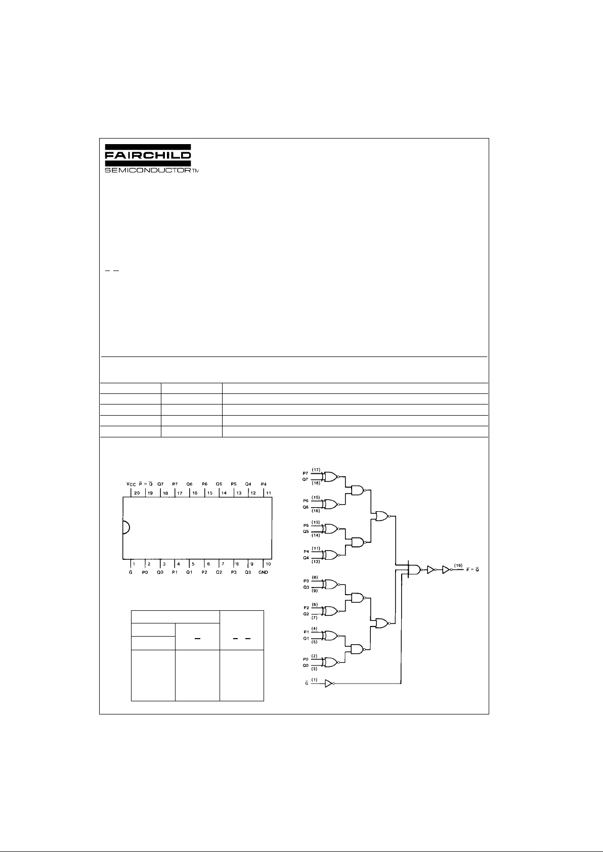
Connection Diagram
Pin Assignments for DIP
Top View
Truth Table
Logic Diagram
Order Number Package Number Package Description
MM74HC688WM M20B 20-Lead Small Outline Integrated Circuit (SOIC), JEDEC MS-013, 0.300” Wide
MM74HC688SJ M20D 20-Lead Small Outline Package (SOP), EIAJ TYPE II, 5.3mm Wide
MM74HC688MTC MTC20 20-Lead Thin Shrink Small Outline Package (TSSOP), JEDEC MO-153, 4.4mm Wide
MM74HC688N N20A 20-Lead Plastic Dual-In-Line Package (PDIP), JEDEC MS-001, 0.300” Wide
Inputs
Data Enable
P,Q
G
P = Q
P = QL L
P > QL H
P < QL H
XHH
Page 2
www.fairchildsemi.com 2
MM74HC688
Absolute Maximum Ratings(Note 1)
(Note 2)
Recommended Operating
Conditions
Note 1: Absolute Maximum Ratings are those values beyond which dam-
age to the device may occur.
Note 2: Unless otherwise specified all voltages are referenced to ground.
Note 3: Power Dissipation temper ature dera ting — plas tic “N” packa ge: −
12 mW/°C from 65 °C to 85°C.
DC Electrical Characteristics (Note 4)
Note 4: For a power supply of 5V ±1 0% the worst c ase ou tput volta ges (VOH, and VOL) occur for HC at 4.5V. Thus the 4. 5V valu es shoul d be use d when
designing with this supply. Worst case V
IH
and VIL occur at V
CC
= 5.5V and 4.5V res pectively. (The VIH value at 5.5V is 3.85V.) The worst case leakage c ur-
rent (I
IN
, ICC, and IOZ) occur for CMOS at the higher voltage and so th e 6. 0V values should be used.
Supply Voltage (VCC) −0.5 to +7.0V
DC Input Voltage (V
IN
) −1.5 to V
CC
+1.5V
DC Output Voltage (V
OUT
) −0.5 to V
CC
+0.5V
Clamp Diode Current (I
IK
, IOK) ±20 mA
DC Output Current, per pin (I
OUT
) ±25 mA
DC V
CC
or GND Current, per pin (ICC) ±50 mA
Storage Temperature Range (T
STG
) −65°C to +150°C
Power Dissipation (P
D
)
(Note 3) 600 mW
S.O. Package only 500 mW
Lead Temperature (T
L
)
(Soldering 10 seconds) 260°C
Min Max Units
Supply Voltage (V
CC
)26V
DC Input or Output Voltage 0 V
CC
V
(V
IN
, V
OUT
)
Operating Temperature Range (T
A
) −40 +85 °C
Input Rise or Fall Times
(t
r
, tf) V
CC
= 2.0V 1000 ns
V
CC
= 4.5V 500 ns
V
CC
= 6.0V 400 ns
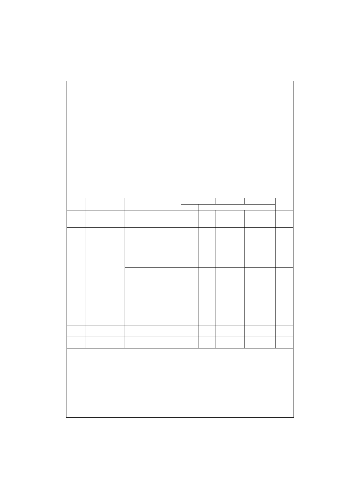
Symbol Parameter Conditions
V
CC
TA = 25°CTA = −40 to 85°CTA = −55 to 125°C
Units
Typ Guaranteed Limits
V
IH
Minimum HIGH Level 2.0V 1.5 1.5 1.5 V
Input Voltage 4.5V 3.15 3.15 3.15 V
6.0V 4.2 4.2 4.2 V
V
IL
Maximum LOW Level 2.0V 0.5 0.5 0.5 V
Input Voltage 4.5V 1.35 1.35 1.35 V
6.0V 1.8 1.8 1.8 V
V
OH
Minimum HIGH Level V
IN
= VIH or V
IL
Output Voltage |I
OUT
| ≤ 20 µA 2.0V 2.0 1.9 1.9 1.9 V
4.5V 4.5 4.4 4.4 4.4 V
6.0V 6.0 5.9 5.9 5.9 V
V
IN
= VIH or V
IL
|I
OUT
| ≤ 4.0 mA 4.5V 4.2 3.98 3.84 3.7 V
|I
OUT
| ≤ 5.2 mA 6.0V 5.7 5.48 5.34 5.2 V
V
OL
Maximum LOW Level V
IN
= VIH or V
IL
Output Voltage |I
OUT
| ≤ 20 µA 2.0V 0 0.1 0.1 0.1 V
4.5V 0 0.1 0.1 0.1 V
6.0V 0 0.1 0.1 0.1 V
V
IN
= VIH or V
IL
|I
OUT
| ≤ 4.0 mA 4.5V 0.2 0.26 0.33 0.4 V
|I
OUT
| ≤ 5.2 mA 6.0V 0.2 0.26 0.33 0.4 V
I
IN
Maximum Input V
IN
= VCC or GND 6.0V ±0.1 ±1.0 ±1.0 µA
Current
I
CC
Maximum Quiescent V
IN
= VCC or GND 6.0V 8.0 80 160 µA
Supply Current I
OUT
= 0 µA
Page 3

3 www.fairchildsemi.com
MM74HC688
AC Electrical Characteristics
V
CC
= 5V, TA = 25°C, CL = 15 pF, tr = t
f
= 6 ns
AC Electrical Characteristics
V
CC
= 2.0V to 6.0V, CL = 50 pF, tr = t
f
= 6 ns (unless otherwise specified)
Note 5: CPD determines the no load dynamic power con s um ption, PD = CPD V
CC
2
f + ICC VCC, and the no load dynam ic current consumpt ion,
I
S
= CPDVCCf + ICC.
Symbol Parameter Conditions Typ
Guaranteed
Units
Limit
t
PHL
, t
PLH
Maximum Propagation 21 30 ns
Delay, any P or Q to Output
t
PLH
, t
PHL
Maximum Propagation 14 20 ns
Delay, Enable to any Output
Symbol Parameter Conditions
V
CC
TA= 25°CTA = −40 to 85°CTA = −55 to 125°C
Units
Typ Guaranteed Limits
t
PHL
, t
PLH
Maximum Propagation 2.0V 60 175 220 263 ns
Delay, P or Q to 4.5V 22 35 44 53 ns
Output 6.0V 19 30 38 45 ns
t
PHL
, t
PLH
Maximum Propagation 2.0V 45 120 150 180 ns
Delay, Enable to 4.5V 15 24 30 36 ns
Output 6.0V 13 20 25 30 ns
t
THL
, t
TLH
Maximum Output Rise 2.0V 30 75 95 110 ns
and Fall Time 4.5V 8 15 19 22 ns
6.0V 7 13 16 19 ns
C
PD
Power Dissipation 45 pF
Capacitance (Note 5)
C
IN
Maximum Input 5 10 10 10 pF
Capacitance
Page 4

www.fairchildsemi.com 4
MM74HC688
Physical Dimensions inches (millimeters) unless otherwise noted
20-Lead Small Outline Integrated Circuit (SOIC), JEDEC MS-013, 0.300” Wide
Package Number M20B
20-Lead Small Outline Package (SOP), EIAJ TYPE II, 5.3mm Wide
Package Number M20D
Page 5

5 www.fairchildsemi.com
MM74HC688
Physical Dimensions inches (millimeters) unless otherwise noted (Continued)
20-Lead Thin Shrink Small Outline Package (TSSOP), JEDEC MO-153, 4.4mm Wide
Package Number MTC20
Page 6

Fairchild does not assume any responsibility for use of any circuitry described, no circuit patent licenses are implied and Fairchild reserves the right at any time without notice to change said circuitry and specifications.
MM74HC688 8-Bit Magnitude Comparator (Equality Detector)
LIFE SUPPORT POLICY
FAIRCHILD’S PRODUCTS ARE NOT AUTHORIZED FOR USE AS CRITICAL COMPONENTS IN LIFE SUPPORT
DEVICES OR SYSTEMS WITHOUT THE EXPRESS WRITTEN APPROVAL OF THE PRESIDENT OF FAIRCHILD
SEMICONDUCTOR CORPORATION. As used herein:
1. Life support devices or systems are devices or syste ms
which, (a) are intended for surgical implant into the
body, or (b) support or sustain life, and (c) whose failure
to perform when properly used in accordance with
instructions for use provided in the labeling, can be reasonably expected to result in a significant inju ry to the
user.
2. A critical component i n any compon ent of a lif e support
device or system whose failu re to perform can be reasonably expected to ca use the fa i lure of the life su pp ort
device or system, or to affect its safety or effectiveness.
www.fairchildsemi.com
Physical Dimensions inches (millimeters) unless otherwise noted (Continued)
20-Lead Plastic Dual-In-Line Package (PDIP), JEDEC MS-001, 0.300” Wide
Package Number N20A
 Loading...