

Datasheet MM74HC597CW, MM74HC597M, MM74HC597N, MM74HC597SJ Datasheet (Fairchild Semiconductor)
Page 1
© 2000 Fairchild Semiconductor Corporation DS005343 www.fairchildsemi.com
January 1988
Revised August 2000
MM74HC597 8-Bit Shift Registers with Input Latches
MM74HC597
8-Bit Shift Registers with Input Latches
General Description
This high speed register utilizes advanced silicon-gate
CMOS technology. It has the high noise immunity and low
power consumption of standard CMO S integrated circuits,
as well as the ability to drive 10 LS-TTL loads.
The MM74HC597 comes in a 16-pin package and consis ts
of an 8-bit storage latch feeding a parallel-in, serial-out
8-bit shift register. Both the storage regis ter and sh ift reg ister have positive-edge triggered clocks. th e shift register
also has direct load (from storage) and clea r inputs .
The 74HC logic family i s sp ee d, fu nctio n, a nd pi n- ou t com patible with the stan dard 74LS logic famil y. All inputs are
protected from dama ge due to static d ischarge by in ternal
diode clamps to V
CC
and ground.
Features
■ 8-bit parallel storage register inputs
■ Wide operating voltage range: 2V–6V
■ Shift register has direct overriding load and clear
■ Guaranteed shift frequency: DC to 30 MHz
■ Low quiescent current: 80
µA maximum
Ordering Code:
Devices also availab le in Tape and Reel. Specify by appending th e s uffix let t er “X” to the ordering code.
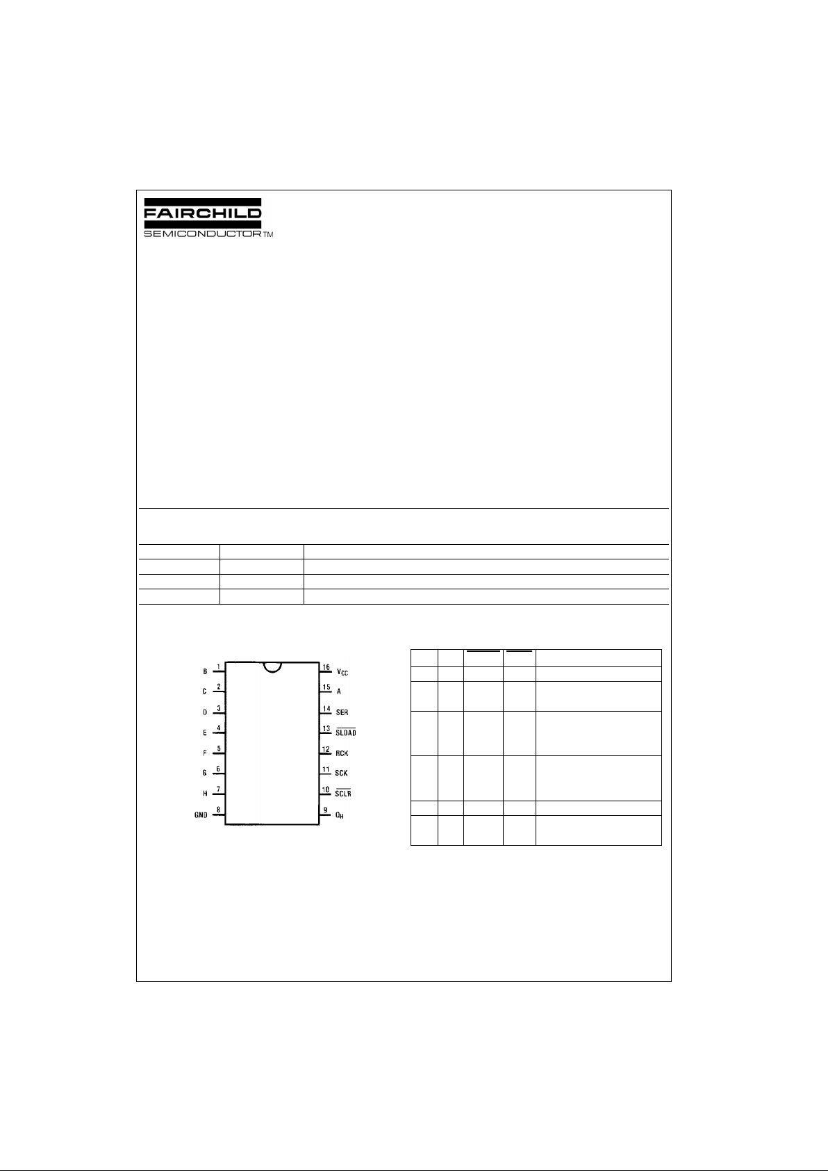
Connection Diagram
Top View
Truth Table
Order Number Package Number Package Description
MM74HC597M M16A 16-Lead Small Outline Integrated Circuit (SOIC), JEDEC MS-012, 0.150 Narrow
MM74HC597SJ M16D 16-Lead Small Outline Package (SOP), EIAJ TYPE II, 5.3mm Wide
MM74HC597N N16E 16-Lead Plastic Dual-In-Line Package (PDIP), JEDEC MS-001, 0.300 Wide
RCK SCK SLOAD SCLR Function
↑ X X X Data Loaded to input latches
↑ XL H
Data loaded from inputs to
shift register
No Data transferred from
clock X L H input latches to shift
edge register
XX L L
Invalid logic, state of
shift register indeterminate
when signals removed
X X H L Shift register cleared
X
↑ HH
Shift register clocked
Q
n
= Q
n
−1, Q
0
= SER
Page 2
www.fairchildsemi.com 2
MM74HC597
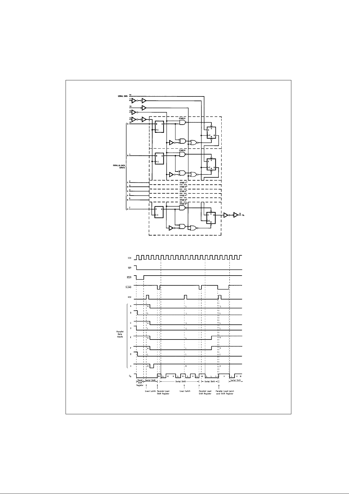
Functional Block Diagram (Positive Logic)
Timing Diagram
Page 3
3 www.fairchildsemi.com
MM74HC597
Absolute Maximum Ratings(Note 1)
(Note 2)
Recommended Operating
Conditions
Note 1: Absolute Maximum Ratings are those values beyond which dam-
age to the device may occur.
Note 2: Unless otherwise specified all voltages are referenced to ground.
Note 3: Power Dissipation te mperature d erating — pl astic “N” package: −
12 mW/°C from 65°C to 85°C.
DC Electrical Characteristics (Note 4)
Note 4: For a power supply of 5V ± 10% the worst case output voltages (VOH, and VOL) occur for HC at 4.5V. Thus the 4.5V values should be used when
designing with this s upply. Worst case V
IH
and VIL occur at V
CC
= 5.5V and 4.5V respectively. (The VIH value at 5.5V is 3.85V.) The worst case leakage cur-
rent (I
IN
, ICC, and IOZ) occur for CMOS at the higher voltage and so th e 6. 0V values should be use d.
Note 5: V
IL
limits are currently te sted at 20% of VCC. The above VIL specification (30% of VCC) will be implemented no later than Q1, CY'89.
Supply Voltage (VCC) −0.5 to +7.0V
DC Input Voltage (V
IN
) −1.5 to V
CC
+1.5V
DC Output Voltage (V
OUT
) −0.5 to V
CC
+0.5V
Clamp Diode Current (I
IK
, IOK) ±20 mA
DC Output Current, per pin (I
OUT
) ±25 mA
DC V
CC
or GND Current, per pin (ICC) ±70 mA
Storage Temperature Range (T
STG
) −65°C to +150°C
Power Dissipation (P
D
)
(Note 3) 600 mW
S.O. Package only 500 mW
Lead Temperature (T
L
)
(Solderi ng 10 seconds ) 260
°C
Min Max Units
Supply Voltage (V
CC
)26V
DC Input or Output Voltage
(V
IN
, V
OUT
)0V
CC
V
Operating Temperature Range (T
A
) −40 +85 °C
Input Rise or Fall Times
(t
r
, tf) V
CC
= 2.0V 1000 ns
V
CC
= 4.5V 500 ns
V
CC
= 6.0V 400 ns
Symbol Parameter Conditions
V
CC
TA = 25°CTA = −40 to 85°CTA = −55 to 125°C
Units
Typ Guaranteed Limits
V
IH
Minimum HIGH Level 2.0V 1.5 1.5 1.5
VInput Voltage 4.5V 3.15 3.15 3.15
6.0V 4.2 4.2 4.2
V
IL
Maximum LOW Level 2.0V 0.5 0.5 0.5
VInput Voltage 4.5V 1.35 1.35 1.35
(Note 5) 6.0V 1.8 1.8 1.8
V
OH
Minimum HIGH Level V
IN
= VIH or V
IL
V
Output Voltage |I
OUT
| ≤ 20 µA 2.0V 2.0 1.9 1.9 1.9
4.5V 4.5 4.4 4.4 4.4
6.0V 6.0 5.9 5.9 5.9
V
IN
= VIH or V
IL
V|I
OUT
| ≤ 4.0 mA 4.5V 4.2 3.98 3.84 3.7
|I
OUT
| ≤ 5.2 mA 6.0V 5.2 5.48 5.34 5.2
V
OL
Maximum LOW Level V
IN
= VIH or V
IL
V
Output Voltage |I
OUT
| ≤ 20 µA 2.0V 0 0.1 0.1 0.1
4.5V 0 0.1 0.1 0.1
6.0V 0 0.1 0.1 0.1
VIN = VIH or V
IL
V|I
OUT
| ≤ 4 mA 4.5V 0.2 0.26 0.33 0.4
|I
OUT
| ≤ 5.2 mA 6.0V 0.2 0.26 0.33 0.4
I
IN
Maximum Input Current V
IN
= VCC or GND 6.0V ±0.1 ±1.0 ±1.0 µA
I
CC
Maximum Quiescent V
IN
= VCC or GND
6.0V 8.0 80 160 µA
Supply Current I
OUT
= 0 µA
Page 4

www.fairchildsemi.com 4
MM74HC597
AC Electrical Characteristics V
CC
= 5V, TA = 25°C, C
L
= 15 pF, t
r
= tf = 6 ns
AC Electrical Characteristics V
CC
= 2.0–6.0V, CL = 50 pF, tr = tf = 6 ns (unless otherwise specified)
Symbol Parameter Conditions Typ
Guaranteed
Units
Limit
f
MAX
Maximum Operating
50 30 MHz
Frequency of SCK
t
PHL
Maximum Propagation
20 30 ns
t
PLH
Delay from SCK to Q
H
t
PHL
Maximum Propagation
20 30 ns
t
PLH
Delay from SLOAD to Q
H
t
PHL
Maximum propagation
SLOAD = logic “0” 25 45 ns
t
PLH
Delay from RCK to Q
H
t
PHL
Maximum Propagation
20 30 ns
Delay from SCLR to Q
H
t
REM
Minimum Removal Time,
10 20 ns
SCLR
to SCK
t
S
Minimum Setup Time
30 40 ns
from RCK to SCK
t
S
Minimum Setup Time
10 20 ns
from SER to SCK
t
S
Minimum Setup Time
10 20 nsfrom inputs A thru H
to RCK
t
H
Minimum Hold Time −20ns
t
W
Minimum Pulse Width
10 16 ns
SCK, RCK, SCLR SLOAD
Symbol Parameter Conditions
V
CC
TA = 25°CTA=−40 to 85°CTA=−55 to 125°C
Units
Typ Guaranteed Limits
f
MAX
Maximum Operating 2.0V 10 6.0 4.8 4.0
MHzFrequency 4.5V 45 30 24 20
6.0V 50 35 28 24
t
PHL
Maximum Propagation 2.0V 62 175 220 263
nst
PLH
Delay from SCK to Q
H
4.5V 20 35 44 53
6.0V 18 30 38 45
t
PHL
Maximum Propagation 2.0V 65 175 220 263
nst
PLH
Delay from SLOAD to Q
H
4.5V 20 35 44 53
6.0V 18 30 38 45
t
PHL
Maximum Propagation 2.0V 120 205 255 310
nst
PLH
Delay from RCK to Q
H
SLOAD = Logic “0” 4.5V 30 41 51 62
6.0V 28 35 43 53
t
PHL
Maximum Propagatin 2.0V 66 175 220 263
nsDelay from SCLR to Q
H
4.5V 20 35 44 53
6.0V 18 30 38 45
t
REM
Minimum Removal Time 2.0V 100 125 150
nsSCLR to SCK 4.5V 20 25 30
6.0V 17 21 25
t
S
Minimum Setup Time 2.0V 200 250 300
nsfrom RCK to SCK 4.5V 40 50 60
6.0V 34 42 50
t
S
Minimum Setup Time 2.0V 100 125 150
nsfrom SER to SCK 4.5V 20 25 30
6.0V 17 21 25
Page 5

5 www.fairchildsemi.com
MM74HC597
AC Electrical Characteristics (Continued)
Note 6: CPD determines the no load dynamic power consumption, PD = CPD V
CC
2
f + ICC VCC, and the no load dynamic current consumption,
I
S
= CPDVCCf + ICC.
Symbol Parameter Conditions
V
CC
TA = 25°CTA=−40 to 85°CTA=−55 to 125°C
Units
Typ Guaranteed Limits
t
S
Minimum Setup Time 2.0V 100 125 150
nsfrom Inputs A thru H 4.5V 20 25 30
to RCK 6.0V 17 21 25
t
H
Minimum Hold Time 2.0V 0 0 0
ns4.5V 0 0 0
6.0V 0 0 0
t
W
Minimum Pulse Width 2.0V 30 80 100 120
ns SCK, RCK, SCLR
, SLOAD 4.5V 9 16 20 24
6.0V 8 14 18 20
t
r
, t
f
Maximum Input Rise and 2.0V 1000 1000 1000
nsFall Time 4.5V 500 500 500
6.0V 400 400 400
t
THL
, t
TLH
Maximum Output 2.0V 30 75 95 110
nsRise and Fall Time 4.5V 10 15 19 22
6.0V 8 13 16 19
t
THL
, t
TLH
Maximum Output 2.0V 75 95 110 ns
Rise and Fall Time 4.5V 15 19 22 ns
6.0V 13 16 19 ns
C
PD
Power Dissipation
87 pF
Capacitance, Outputs (Note 6)
C
IN
Maximum Input
510 10 10pF
Capacitance
C
OUT
Maximum Output
15 20 20 20 pF
Capacitance
Page 6

www.fairchildsemi.com 6
MM74HC597
Physical Dimensions inches (millimeters) unless otherwise noted
16-Lead Small Outline Integrated Circuit (SOIC), JEDEC MS-012, 0.150 Narrow
Package Number M16A
Page 7

7 www.fairchildsemi.com
MM74HC597
Physical Dimensions inches (millimeters) unless otherwise noted (Continued)
16-Lead Small Outline Package (SOP), EIAJ TYPE II, 5.3mm Wide
Package Number M16D
Page 8

www.fairchildsemi.com 8
MM74HC597 8-Bit Shift Registers with Input Latches
Physical Dimensions inches (millimeters) unless otherwise noted (Continued)
16-Lead Plastic Dual-In-Line Package (PDIP), JEDEC MS-001, 0.300 Wide
Package Number N16E
Fairchild does not assume any responsibility for use of any circuitr y described, no circuit patent licenses are implied and
Fairchild reserves the right at any time without notice to change said circuitry and specifications.
LIFE SUPPORT POLICY
FAIRCHILD’S PRODUCTS ARE NOT AUTHORIZED FOR USE AS CRITICAL COMPONENTS IN LIFE SUPPORT
DEVICES OR SYSTEMS WITHOUT THE EXPRESS WRITTEN APPROVAL OF THE PRESIDENT OF FAIRCHILD
SEMICONDUCTOR CORPORATION. As used herein:
1. Life support devices or systems are devices or syste ms
which, (a) are intended for surgical implant into the
body, or (b) support or sustain life, and (c) whose failure
to perform when properly used in accordance with
instructions for use provided in the labeling, can be reasonably expected to result in a significant inju ry to the
user.
2. A critical component in any compon ent of a lif e supp ort
device or system whose failure t o perform can be reasonably expected to ca use the failure of the life supp ort
device or system, or to affect its safety or effectiveness.
www.fairchildsemi.com
 Loading...