

Page 1
January 1992
Revised May 1999
MM74HC594 8-Bit Shift Register with Output Registers
© 1999 Fairchild Semiconductor Corporation DS010915.prf www.fairchildsemi.com
MM74HC594
8-Bit Shift Register with Output Registers
General Description
This high speed shift register utilizes advanced silicon-gate
CMOS technology. This device possesses the high noise
immunity and low power c onsumption of standard CMOS
integrated circuits, as well as the ability to drive 15 LS-TT L
loads.
This device contains an 8-bit serial-in, parallel-out shift register that feeds an 8-bit D-type storage register. Separate
clocks and direct overriding clears are provided for both the
shift register and the storage register. The shift register has
a direct-overriding clear, serial input, and serial output
(standard) pins for casca ding. Both the shift register and
storage register use posit ive-edge tr iggered clocks. I f both
clocks are connected toget her, the shift register state will
always be one clock pulse ahead of the storage register.
The 74HC logic family is speed, function, an d p in-o ut co mpatible with the sta ndard 74LS logic fami ly. All inputs are
protected from damage due to static discharge by inte rnal
diode clamps to V
CC
and ground.
Features
■ Low quiescent current: 80 µA maximum
■ Low input current: 1 µA maximum
■ 8-bit serial-in, parallel-out shift register with storage
■ Wide operating voltage range: 2V to 6V
■ Cascadable
■ Shift register has direct clear
■ Guaranteed shift frequency: DC to30 MHz
Ordering Code:
Devices also availab le in Tape and Reel. Specify by appending th e s uffix let t er “X” to the ordering cod e.
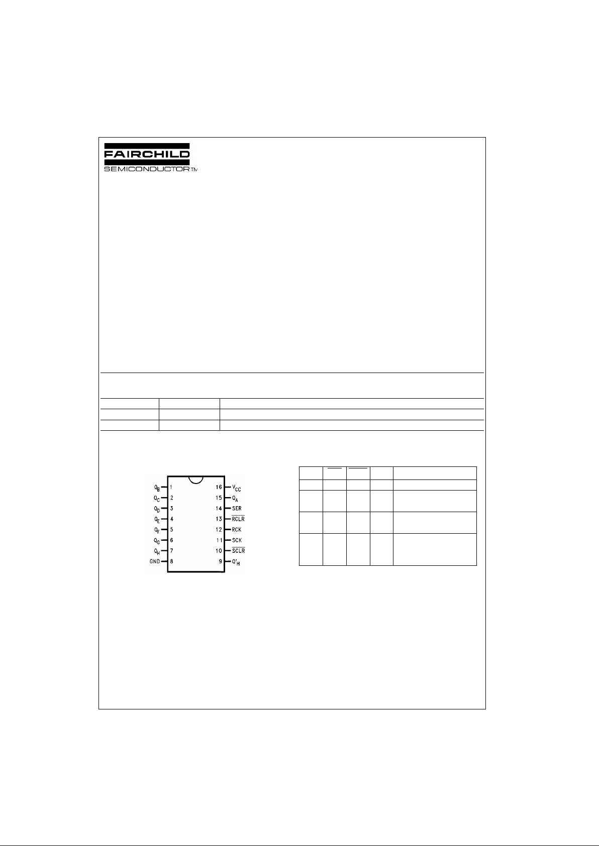
Connection Diagram Truth Table
Order Number Package Number Package Description
MM74HC594M M16A 16-Lead Small Outline Integrated Circuit (SOIC), JEDEC MS-012, 0.150 Narrow
MM74HC594N N16E 16-Lead Plastic Dual-In-Line Package (PDIP), JEDEC MS-001, 0.300 Wide
RCK SCK SCLR RCLR Function
X X X L Storage Register cleared
XXLX
Shift Register cleared
Q’
H
= 0
X ↑ HH
Shift Register clocked
Q
N
= Q
n−1
, Q0 = SER
↑ XHH
Contents of Shift
Register transferred
to output latches
Page 2
www.fairchildsemi.com 2
MM74HC594
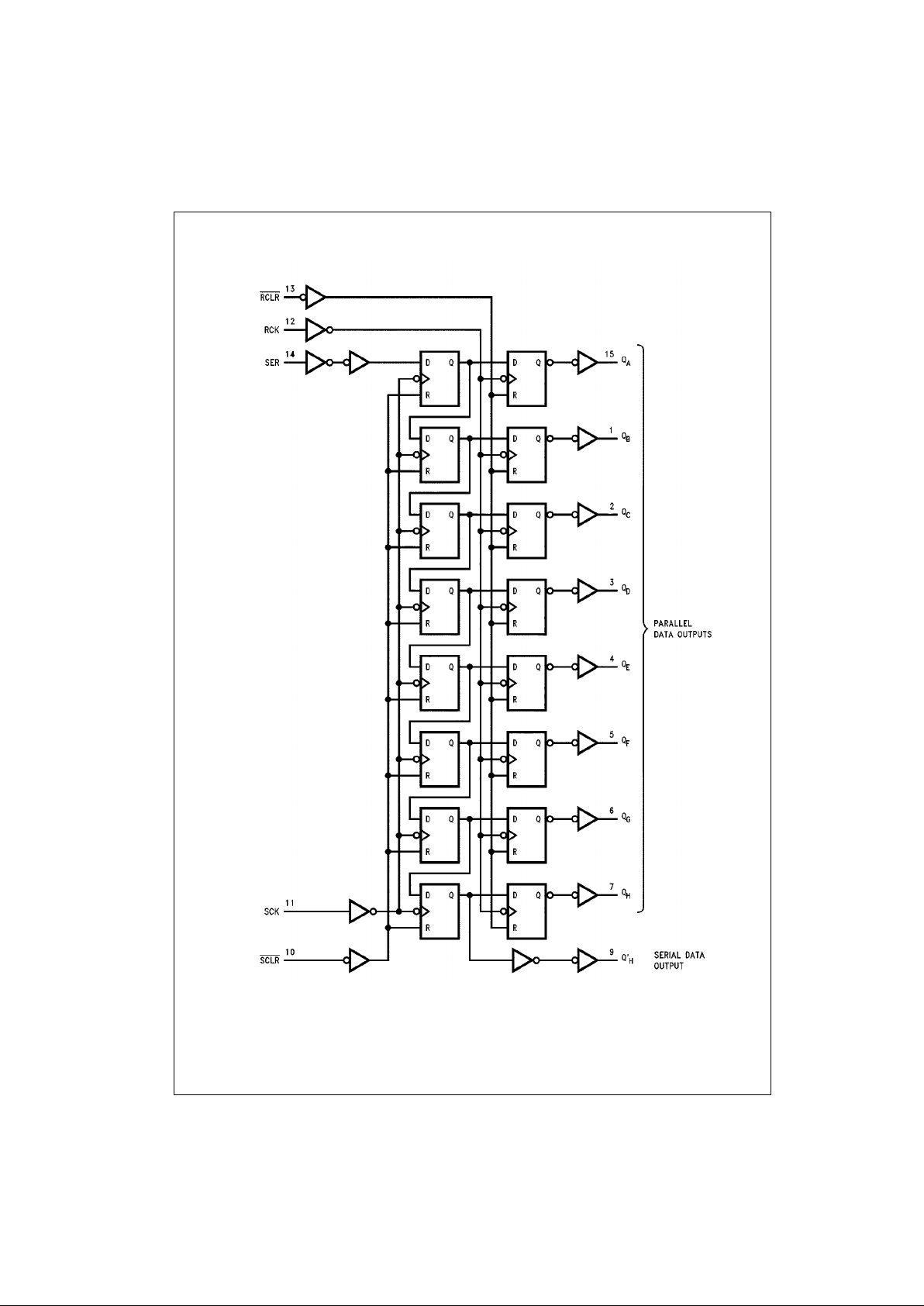
Logic Diagram
Page 3
3 www.fairchildsemi.com
MM74HC594
Absolute Maximum Ratings(Note 1)
(Note 2)
Recommended Operation
Conditions
Note 1: Absolute Maximum Ra tings are those valu es beyond w hich dam-
age to the device may occur.
Note 2: Unless otherwise specified all voltages are referenced to ground.
Note 3: Power Dissipation temperature derating—plastic “N” pac k age: −12
mW/°C from 65°C to 85°C.
DC Electrical Characteristics (Note 4)
Note 4: For a powe r supply o f 5V ±10% the worst case output voltages (VOH, and VOL) occur for HC at 4.5V. Thus the 4. 5V valu es shou ld be u sed when
designing with this supply. Worst case V
IH
and VIL occur at VCC = 5.5V and 4.5 V respectively. (The VIH value at 5.5V is 3.85V.) The worst case leakage cur-
rent (I
IN
, ICC, and IOZ) occur for CMOS at the higher voltage and so th e 6. 0V values should be used.
Supply Voltage (VCC) −0.5 to +7.0V
DC Input Voltage (V
IN
) −1.5 to VCC +1.5V
DC Output Voltage (V
OUT
) −0.5 to VCC +0.5V
Clamp Diode Current (I
IK
, IOK) ±20 mA
DC Output Current, per pin (I
OUT
) ±35 mA
DC V
CC
or GNDCurrent,per pin(ICC) ±70 mA
Storage Temperature Range (T
STG
) −65°C to +150°C
Power Dissipation (P
D
)
(Note 3) 600 mW
S.O. Package only 500 mW
Lead Temperature (T
L
)
(Soldering 10 seconds) 260°C
Min Max Units
Supply Voltage (V
CC
)26V
DC Input or Output Voltage 0 V
CC
V
(V
IN
, V
OUT
)
Operating Temperature Range (T
A
) −40 +85 °C
Input Rise or Fall Times
(t
r
, tf)VCC = 2.0V 1000 ns
V
CC
= 4.5V 500 ns
V
CC
= 6.0V 400 ns
Symbol Parameter Conditions
V
CC
TA = 25°CT
A
= −40 to 85°C
Units
Typ Guaranteed Limits
V
IH
Minimum HIGH Level 2.0V 1.5 1.5
VInput Voltage 4.5V 3.15 3.15
6.0V 4.2 4.2
V
IL
Maximum LOW Level 2.0V 0.5 0.5
VInput Voltage 4.5V 1.35 1.35
6.0V 1.8 1.8
V
OH
Minimum HIGH Level VIN = VIH or V
IL
V
Output Voltage |I
OUT
| ≤ 20 µA 2.0V 2.0 1.9 1.9
4.5V 4.5 4.4 4.4
6.0V 6.0 5.9 5.9
Q’
H
VIN = VIH or V
IL
V|I
OUT
| ≤ 4.0 mA 4.5V 4.7 3.98 3.84
|I
OUT
| ≤ 5.2 mA 6.0V 5.2 5.48 5.34
QA thru Q
H
VIN = VIH or V
IL
V|I
OUT
| ≤ 6.0 mA 4.5V 4.2 3.98 3.84
|I
OUT
| ≤ 7.8 mA 6.0V 5.7 5.48 5.34
V
OL
Maximum LOW Level VIN = VIH or V
IL
V
Output Voltage |I
OUT
| ≤ 20 µA2.0V00.10.1
4.5V 0 0.1 0.1
6.0V 0 0.1 0.1
Q’
H
VIN = VIH or V
IL
V|I
OUT
| ≤ 4.0 mA 4.5V 0.2 0.26 0.33
|I
OUT
| ≤ 5.2 mA 6.0V 0.2 0.26 0.33
QA thru Q
H
VIN = VIH or V
IL
V|I
OUT
| ≤ 6.0 mA 4.5V 0.2 0.26 0.33
|I
OUT
| ≤ 7.8 mA 6.0V 0.2 0.26 0.33
I
IN
Maximum Input VIN = VCC or GND 6.0V ±0.1 ±1.0 µA
Current
I
CC
Maximum Quiescent VIN = VCC or GND 6.0V 8.0 80 µA
Supply Current I
OUT
= 0 µA
Page 4

www.fairchildsemi.com 4
MM74HC594
AC Electrical Characteristics
VCC = 2.0V to 6.0V, CL = 50 pF, tr = tf = 6 ns (unless otherwise specified)
Symbol Parameter Conditions
V
CC
TA = 25°C
−40°C to +85°C
Units
Typ Guaranteed Limits
f
MAX
Maximum Operating CL = 50 pF 2.0V 6 4.8
MHzFrequency 4.5V 30 24
6.0V 35 28
t
PHL
, t
PLH
Maximum Propagation Delay CL = 50 pF 2.0V 150 185
nsfrom SCK to Q’
H
4.5V 30 37
6.0V 25 31
t
PHL
, t
PLH
Maximum Propagation Delay CL = 50 pF 2.0V 150 185
ns
from RCK to QA thru Q
H
CL = 150 pF 2.0V 200 250
CL = 50 pF 4.5V 30 37
ns
CL = 150 pF 4.5V 40 50
CL = 50 pF 6.0V 25 31
ns
CL = 150 pF 6.0V 34 43
t
PHL
, t
PLH
Maximum Propagation Delay 2.0V 150 185
ns
from SCLR to Q’
H
4.5V 30 37
6.0V 25 31
t
PHL
Maximum Propagation Delay CL = 50 pF 2.0V 125 155
ns
from RCLR to QA thru Q
H
4.5V 25 31
6.0V 21 26
CL = 150 pF 2.0V 200 250
ns4.5V 40 50
6.0V 34 43
t
S
SCLR LOW to RCK
2.0V 50 63
ns
4.5V 10 13
6.0V 9 11
t
S
RCLR HIGH to SCK
2.0V 5 5
ns
4.5V 5 5
6.0V 5 5
t
S
Minimum Setup Time 2.0V 90 110
nsfrom SER to SCK 4.5V 18 22
6.0V 15 19
t
R
Minimum Removal Time 2.0V 20 20
ns
from SCLR to SCK
4.5V 10 10
6.0V 10 10
t
S
Minimum Setup Time 2.0V 90 110
nsfrom SCK to RCK 4.5V 18 22
6.0V 15 19
t
H
Minimum Hold Time 2.0V 5 5
nsSER to SCK 4.5V 5 5
6.0V 5 5
t
W
Minimum Pulse Width 2.0V 100 125
nsof SCK or SCLR or
4.5V 20 25
RCK or RCLR
6.0V 17 21
tr, t
f
Maximum Input Rise and 2.0V 1000 1000
nsFall Time, Clock 4.5V 500 500
6.0V 400 400
t
THL
, t
TLH
Maximum Output 2.0V 60 75
nsRise and Fall Time 4.5V 12 15
QA - Q
H
6.0V 10 13
t
THL
, t
TLH
Maximum Output 2.0V 75 95
nsRise and Fall Time 4.5V 15 19
Q’
H
6.0V 13 16
Page 5

5 www.fairchildsemi.com
MM74HC594
AC Electrical Characteristics (Continued)
Note 5: CPD determines the no load dynamic power con s um ption, and the no load dy namic current consum pt ion.
Symbol Parameter Conditions
V
CC
TA = 25°C
−40°C to +85°C
Units
Typ Guaranteed Limits
C
PD
Power Dissipation Capacitance,
G = V
CC
90
pF
Outputs Enabled (Note 5)
G = GND
150
C
IN
Maximum Input Capacitance 5 10 10 pF
C
OUT
Maximum Output Capacitance 15 20 20 pF
Page 6

www.fairchildsemi.com 6
MM74HC594
Physical Dimensions inches (millimeters) unless otherwise noted
16-Lead Small Outline Integrated Circuit (SOIC), JEDEC MS-012, 0.150 Narrow
Package Number M16A
Page 7

Fairchild does not assume any responsibility for use of any circuitry described, no circuit patent licenses are implied and Fairchild reserves the right at any time without notice to change said circuitry and specifications.
MM74HC594 8-Bit Shift Register with Output Registers
LIFE SUPPORT POLICY
FAIRCHILD’S PRODUCTS ARE NOT AUTHORIZED FOR USE AS CRITICAL COMPONENTS IN LIFE SUPPORT
DEVICES OR SYSTEMS WITHOUT THE EXPRESS WRITTEN APPROVAL OF THE PRESIDENT OF FAIRCHILD
SEMICONDUCTOR CORPORATION. As used herein:
1. Life support devices or systems are devices or syste ms
which, (a) are intended for surgical implant into the
body, or (b) support or sustain life, and (c) whose failure
to perform when properly used in accordance with
instructions for use provided i n the labe li ng, can be re asonably expected to result in a significant injury to the
user.
2. A critical component in any compo nent o f a li fe supp ort
device or system whose failu re to perform can b e reasonably expected to c ause th e fa i lure of the li fe s upp or t
device or system, or to affect its safety or effectiveness.
www.fairchildsemi.com
Physical Dimensions inches (millimeters) unless otherwise noted (Continued)
16-Lead Plastic Dual-In-Line Package (PDIP), JEDEC MS-001, 0.300 Wide
Package Number N16E
 Loading...