

Datasheet MM74HC589SJ, MM74HC589MX, MM74HC589SJX, MM74HC589N, MM74HC589M Datasheet (Fairchild Semiconductor)
Page 1
September 1983
Revised February 1999
MM74HC589 8-Bit Shift Registers with Input Latches and 3-STATE Serial Output
© 1999 Fairchild Semiconductor Corporation DS005368.prf www.fairchildsemi.com
MM74HC589
8-Bit Shift Registers with Input Latches and 3-STATE
Serial Output
General Description
The MM74HC589 high speed shift register utilizes
advanced silicon-gate CMOS technology to achieve the
high noise immunity and low power consumption of standard CMOS integrated circuits, as well as the ability to
drive 15 LS-TTL loads.
The MM74HC589 comes in a 16-p in pa ckag e an d con s ists
of an 8-bit storage latch feeding a parall el-in, serial-out 8bit shift register. Data can also be entered seriall y the shift
register through the SER pin. Both the storage register and
shift register have positive-edge triggered clocks, RCK and
SCK, respectively. SLOAD
pin controls parallel LOAD or
serial shift operations for the shift register. The shift register
has a 3-STATE output to enabl e th e wi re -ORi n g o f mu l tiple
devices on a serial bus.
The 74HC logic family is speed, function, an d p in-o ut co mpatible with the sta ndard 74LS logic fami ly. All inputs are
protected from damage due to static discharge by inte rnal
diode clamps to V
CC
and ground.
Features
■ 8-bit parallel storag e register inputs
■ Wide operating voltage range: 2V–6V
■ Shift register has direct overriding load
■ Guaranteed shift frequency. . . DC to 30 MHz
■ Low quiescent current: 80 µA maximum (74HC Series)
■ 3-STATE output for ‘Wire-OR'
Ordering Code:
Devices also availab le in Tape and Reel. Specify by appending th e s uffix let t er “X” to the ordering cod e.
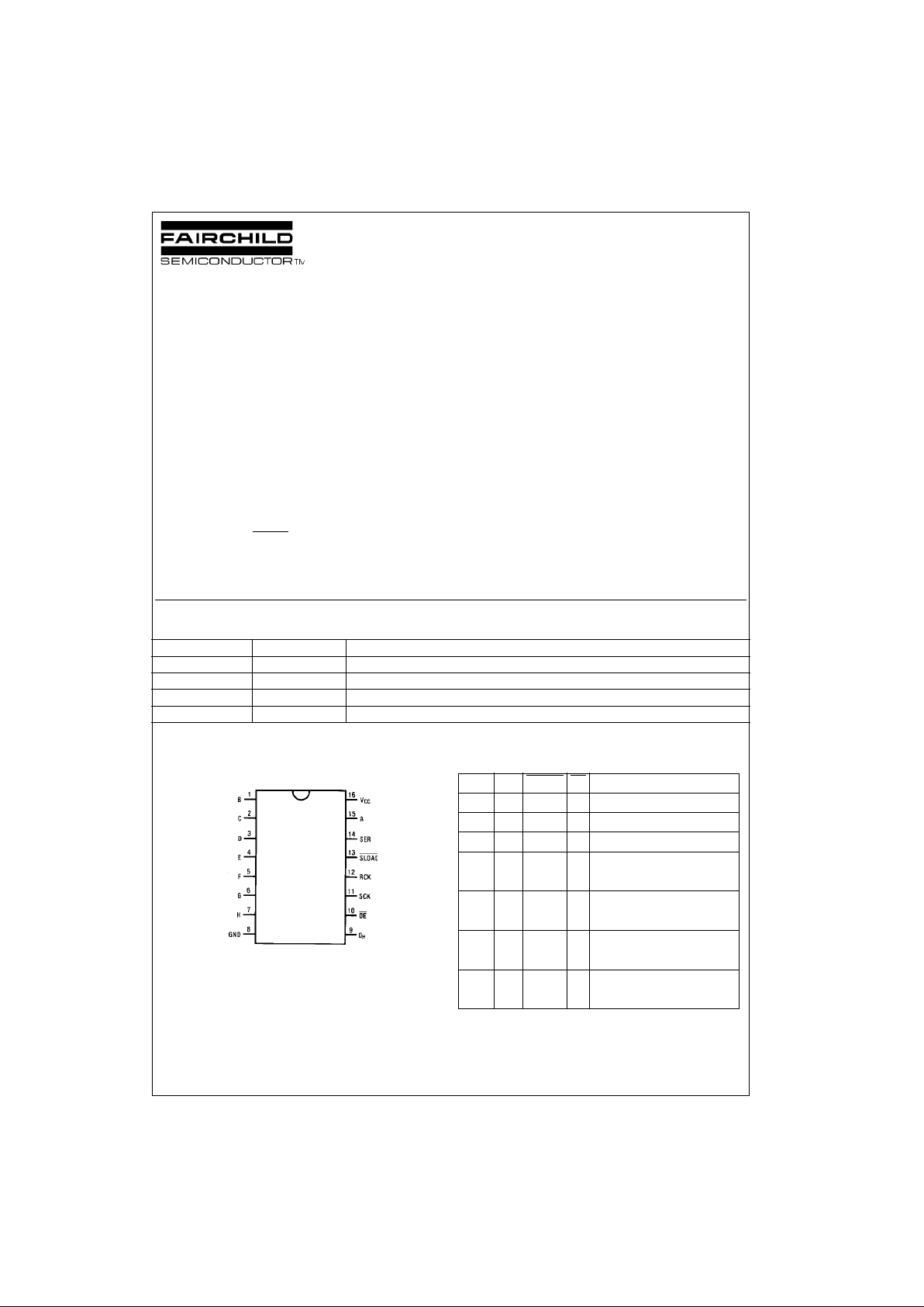
Connection Diagram
Pin Assignments f or DIP, SOIC, SOP and TSSOP
Top View
Truth Table
Order Number Package Number Package Description
MM74HC589M M16A 16-Lead Small Outline Integrated Circuit (SOIC), JEDEC MS-012, 0.150” Narrow
MM74HC589SJ M16D 16-Lead Small Outline Package (SOP), EIAJ TYPE II, 5.3mm Wide
MM74HC589MTC MTC16 16-Lead Thin Shrink Small Outline Package (TSSOP), JEDEC MO-153, 4.4mm Wide
MM74HC589N N16E 16-Lead Plastic Dual-In-Line Package (PDIP), JEDEC MS-001, 0.300” Wide
RCK SCK SLOAD OE Function
XX XHQ
H
in Hi-Z State
XX XLQ
H
is enabled
↑ X X X Data loaded into input latches
↑ X L X Data loaded into shift register
from pins
H or L X L X Data loaded from latches to
shift register
X ↑ H X Shift register is shifted. Data
on SER pin is shifted in.
↑↑ H X Data is shifted in shift register,
and data is loaded into latches
Page 2
www.fairchildsemi.com 2
MM74HC589
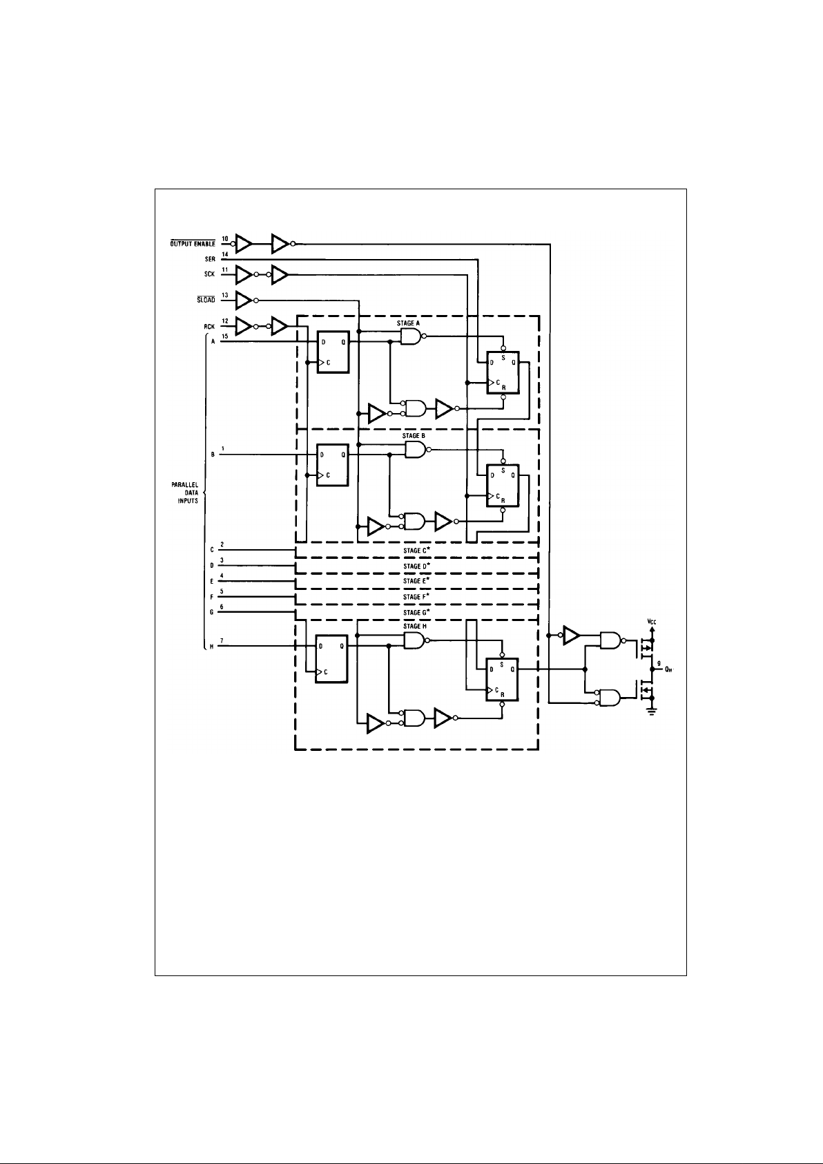
Block Diagram (positive logic)
Page 3
3 www.fairchildsemi.com
MM74HC589
Absolute Maximum Ratings(Note 1)
(Note 2)
Recommended Operating
Conditions
Note 1: Absolute Maximum Ra tings are those valu es beyond w hich dam-
age to the device may occur.
Note 2: Unless otherwise specified all voltages are referenced to ground.
Note 3: Power Dissipation te mperature d erating — pl astic “N” pa ckage: −
12 mW/°C from 65°C to 85°C.
DC Electrical Characteristics (Note 4)
Note 4: For a powe r supply o f 5V ±10% the worst case output voltages (VOH, and VOL) occur for HC at 4.5V. Thus the 4. 5V valu es shou ld be u sed when
designing with this supply. Worst case V
IH
and VIL occur at VCC=5.5V and 4.5V respectively. (The VIH value at 5.5V is 3. 85V.) The wor st c ase le ak ag e cur ren t
(I
IN
, ICC, and IOZ) occur for CMOS at the higher voltage and s o t he 6.0V values should be used.
Supply Voltage (VCC) −0.5 to +7.0V
DC Input Voltage (V
IN
) −1.5 to V
CC
+1.5V
DC Output Voltage (V
OUT
) −0.5 to V
CC
+0.5V
Clamp Diode Current (I
IK
, IOK) ±20 mA
DC Output Current, per pin (I
OUT
) ±25 mA
DC V
CC
or GND Current, per pin (ICC) ±50 mA
Storage Temperature Range (T
STG
) −65°C to +150°C
Power Dissipation (P
D
)
(Note 3) 600 mW
S.O. Package only 500 mW
Lead Temperature (T
L
)
(Soldering 10 second s) 260°C
Min Max Units
Supply Voltage (V
CC
)26V
DC Input or Output Voltage
(V
IN
, V
OUT
)0V
CC
V
Operating Temperature Range (T
A
) −40 +85 °C
Input Rise or Fall Times
(t
r
, tf) V
CC
= 2.0V 1000 ns
V
CC
= 4.5V 500 ns
V
CC
= 6.0V 400 ns
Symbol Parameter Conditions
V
CC
TA = 25°CTA = −40 to 85°CTA = −55 to 125°C
Units
Typ Guaranteed Limits
V
IH
Minimum HIGH Level 2.0V 1.5 1.5 1.5 V
Input Voltage 4.5V 3.15 3.15 3.15 V
6.0V 4.2 4.2 4.2 V
V
IL
Maximum LOW Level 2.0V 0.5 0.5 0.5 V
Input Voltage 4.5V 1.35 1.35 1.35 V
6.0V 1.8 1.8 1.8 V
V
OH
Minimum HIGH Level V
IN
= VIH or V
IL
Output Voltage |I
OUT
| ≤ 20 µA 2.0V 2.0 1.9 1.9 1.9 V
4.5V 4.5 4.4 4.4 4.4 V
6.0V 6.0 5.9 5.9 5.9 V
V
IN
= VIH or V
IL
|I
OUT
| ≤ 6.0 mA 4.5V 3.98 3.84 3.7 V
|I
OUT
| ≤ 7.8 mA 6.0V 5.48 5.34 5.2 V
V
OL
Maximum LOW Level V
IN
= VIH or V
IL
Output Voltage |I
OUT
| ≤ 20 µA 2.0V 0 0.1 0.1 0.1 V
4.5V 0 0.1 0.1 0.1 V
6.0V 0 0.1 0.1 0.1 V
V
IN
= VIH or V
IL
|I
OUT
| ≤ 6.0 mA 4.5V 0.26 0.33 0.4 V
|I
OUT
| ≤ 7.8 mA 6.0V 0.26 0.33 0.4 V
I
IN
Maximum Input V
IN
= VCC or GND 6.0V ±0.1 ±1.0 ±1.0 µA
Current
I
CC
Maximum Quiescent V
IN
= VCC or GND 6.0V 8.0 80 160 µA
Supply Current I
OUT
= 0 µA
I
OZ
Maximum 3-STATE Output in High 6.0V ±0.5 ±5.0 ±10.0 µA
Leakage Current Impedance State
VIN = VIL or V
IH
V
OUT
= VCC or GND
OE = V
IH
Page 4

www.fairchildsemi.com 4
MM74HC589
AC Electrical Characteristics
V
CC
= 5V, T
A
= 25°C, C
L
= 15 pF, tr = t
f
= 6 ns
AC Electrical Characteristics
V
CC
= 2.0−6V, CL = 50 pF, tr = t
f
= 6 ns (unless otherwise specified)
Symbol Parameter Conditions Typ
Guaranteed
Limit
Units
f
MAX
Maximum Operating Frequency for SCK 50 30 MHz
t
PHL
, t
PLH
Maximum Propagation Delay from SCK to Q
H’
30 ns
t
PHL
, t
PLH
Maximum Propagation Delay from SLOAD to Q
H’
30 ns
t
PHL
, t
PLH
Maximum Propagation Delay from LCK to Q
H’
SLOAD = logic “0”
25 45 ns
t
PZH
, t
PZL
Output Enable Time RL = 1 kΩ 18 28 ns
t
PHZ
, t
PLZ
Output Disable Time RL = 1 kΩ, CL = 5 pF 19 25 ns
t
S
Minimum Setup Time from RCK to SCK 10 20 ns
t
S
Minimum Setup Time from SER to SCK 10 20 ns
t
S
Minimum Setup Time from Inputs A thru H to RCK 10 20 ns
t
H
Minimum Hold Time 0 5 ns
t
W
Minimum Pulse Width SCK, RCK, SLOAD
816ns
Symbol Parameter Conditions
V
CC
TA = 25°CTA = −40 to 85°CTA = −55 to 125°C
Units
Typ Guaranteed Limits
f
MAX
Maximum Operating 2.0V 6 4.8 4 MHz
Frequency for SCK 4.5V 30 24 20 MHz
6.0V 35 28 24 MHz
t
PHL
, t
PLH
Maximum Propagation 2.0V 62 175 220 265 ns
Delay from SCK or 4.5V 20 35 44 53 ns
SLOAD to Q
H
6.0V 18 30 37 45 ns
t
PHL
, t
PLH
Maximum Propagation 2.0V 120 225 280 340 ns
Delay from SCK or CL = 150 pF 4.5V 31 45 56 68 ns
SLOAD to Q
H
6.0V 28 38 48 58 ns
t
PHL
, t
PLH
Maximum Propagation 2.0V 80 210 265 315 ns
Delay from RCK to Q
H
4.5V 25 42 53 63 ns
6.0V 21 36 45 54 ns
t
PHL
, t
PLH
Maximum Propagation 2.0V 80 210 265 313 ns
Delay RCK to Q
H
CL = 150 pF 4.5V 25 52 66 77 ns
6.0V 21 44 56 66 ns
t
PZH
, t
PZL
Output Enable Time RL = 1 kΩ 2.0V 70 150 189 224 ns
4.5V 22 30 38 45 ns
6.0V 20 26 32 38 ns
t
PHZ
, t
PLZ
Output Disable Time RL = 1 kΩ 2.0V 70 150 189 224 ns
4.5V 22 30 38 45 ns
6.0V 20 26 32 38 ns
t
S
Minimum Setup Time 2.0V 100 125 150 ns
from RCK to SCK 4.5V 20 25 30 ns
6.0V 17 22 25 ns
t
S
Minimum Setup Time 2.0V 100 125 150 ns
from SER to SCK 4.5V 20 25 30 ns
6.0V 17 22 25 ns
t
S
Minimum Setup Time 2.0V 100 125 150 ns
from Inputs A thru H 4.5V 20 25 30 ns
to RCK 6.0V 17 22 25 ns
t
H
Minimum Hold Time 2.0V −55 5 5 ns
4.5V 0 5 5 5 ns
6.0V 1 5 5 5 ns
t
W
Minimum Pulse Width 2.0V 30 80 100 120 ns
SCK, RCK, SLOAD,
4.5V 9 16 20 24 ns
SLOAD
6.0V 8 14 17 20 ns
Page 5

5 www.fairchildsemi.com
MM74HC589
AC Electrical Characteristics (Continued)
Note 5: CPD determines the no load dynamic power con s um ption, PD = CPD V
CC
2
f + ICC VCC, and the no load dynam ic current consumpt ion,
I
S
= CPDVCCsf + ICC.
Symbol Parameter Conditions
V
CC
TA = 25°CTA = −40 to 85°CTA = −55 to 125°C
Units
Typ Guaranteed Limits
tr, t
f
Maximum Input Rise and 2.0V 1500 1500 1500 ns
Fall Time, Clock 4.5V 500 500 500 ns
6.0V 400 400 400 ns
t
THL
, t
TLH
Maximum Output 2.0V 25 60 75 90 ns
Rise and Fall Time 4.5V 6 12 15 18 ns
6.0V 5 10 12 15 ns
C
PD
Power Dissipation 87 pF
Capacitance (Note 5)
C
IN
Maximum Input Capacitance 5 10 10 10 pF
C
OUT
Maximum Output Capacitance 15 20 20 20 pF
Page 6

www.fairchildsemi.com 6
MM74HC589
Timing Diagram
Page 7

7 www.fairchildsemi.com
MM74HC589
Physical Dimensions inches (millimeters) unless otherwise noted
16-Lead Small Outline Integrated Circuit (SOIC), JEDEC MS-012, 0.150” Narrow
Package Number M16A
16-Lead Small Outline Package (SOP), EIAJ TYPE II, 5.3mm Wide
Package Number M16D
Page 8

www.fairchildsemi.com 8
MM74HC589
Physical Dimensions inches (millimeters) unless otherwise noted (Continued)
16-Lead Thin Shrink Small Outline Package (TSSOP), JEDEC MO-153, 4.4mm Wide
Package Number MTC16
Page 9

Fairchild does not assume any responsibility for use of any circuitry described, no circuit patent licenses are implied and Fairchild reserves the right at any time without notice to change said circuitry and specifications.
MM74HC589 8-Bit Shift Registers with Input Latches and 3-STATE Serial Output
LIFE SUPPORT POLICY
FAIRCHILD’S PRODUCTS ARE NOT AUTHORIZED FOR USE AS CRITICAL COMPONENTS IN LIFE SUPPORT
DEVICES OR SYSTEMS WITHOUT THE EXPRESS WRITTEN APPROVAL OF THE PRESIDENT OF FAIRCHILD
SEMICONDUCTOR CORPORATION. As used herein:
1. Life suppor t de vices o r syst ems are devices or systems
which, (a) are intended for surgical implant into the
body, or (b) support or sustain life, and (c) whose failure
to perform when properly used in accordance with
instructions for use provided i n the labe li ng, can be re asonably expected to result in a significant injury to the
user.
2. A crit ical com ponen t in any com ponent o f a l ife supp ort
device or system whose failu re to perform can b e reasonably expected to c ause th e fa i lure of the li fe s upp or t
device or system, or to affect its safety or effectiveness.
www.fairchildsemi.com
Physical Dimensions inches (millimeters) unless otherwise noted (Continued)
16-Lead Plastic Dual-In-Line Package (PDIP), JEDEC MS-001, 0.300” Wide
Package Number N16E
 Loading...