

Datasheet MM74HC4514WMX, MM74HC4514N, MM74HC4514WM, MM74HC4514MTC Datasheet (Fairchild Semiconductor)
Page 1
© 2000 Fairchild Semiconductor Corporation DS005215 www.fairchildsemi.com
February 1984
Revised February 2000
MM74HC4514 4-to-16 Line Decoder with Latch
MM74HC4514
4-to-16 Line Decoder with Latch
General Description
The MM74HC4514 utilizes advanced silicon-gate CMOS
technology, which is well suited to memory address decoding or data routing application. It possesses high noise
immunity and low power dissipation usually associated with
CMOS circuitry, yet speeds comparable to low power
Schottky TTL circuits. It can drive up to 10 LS-TTL loads.
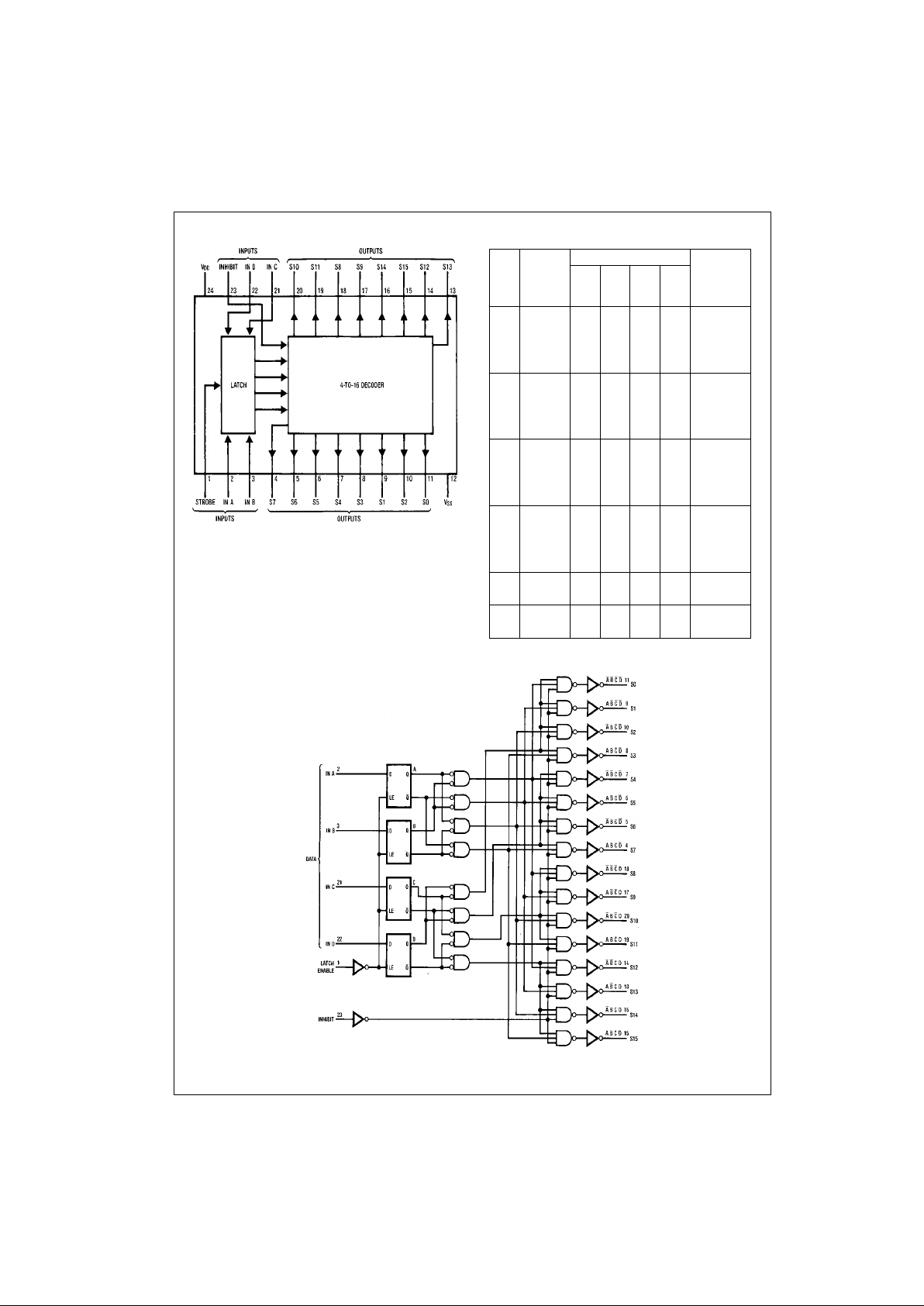
The MM74HC4514 contain a 4-to-16 line d eco der and a 4bit latch. The latch can store the da ta on the select i nputs,
thus allowing a selected output to remain HIGH even
though the select data has changed. When the LATCH
ENABLE input to the latches is HIGH the outputs will
change with the inputs. Whe n LATCH ENABLE goes LOW
the data on the select inputs is stored in the latches. T he
four select inputs determine which output will go HIGH provided the INHIBIT input is LOW. If the INHIBIT input is
HIGH all outputs are held LOW thus disabling the decoder.
The MM74HC4514 is func tionally and p inout equ ivalent to
the CD4514BC and the MC1451BC. All inputs are protected against damage due to static discharge diodes from
V
CC
and ground.
Features
■ Typical propagation delay: 18 ns
■ Low quiescent power: 80 µA maximum (74HC Series)
■ Low input current: 1 µA maximum
■ Fanout of 10 LS-TTL loads (74HC Series)
Ordering Code:
Devices also availab le in Tape and Reel. Specify by appending th e s uffix let t er “X” to the ordering code.
Order Number Package Number Package Description
MM74HC4514WM M24B 24-Lead Small Outline Integrated Circuit (SOIC), JEDEC MS-0013, 0.300” Wide
MM74HC4514MTC MTC24 24-Lead Thin Shrink Small Outline Package (TSSOP), JEDEC MO-153, 4.4mm Wide
MM74HC4514N N24C 24-Lead Plastic Dual-In-Line Package (PDIP), JEDEC MS-100, 0.300” Wide
Page 2
www.fairchildsemi.com 2
MM74HC4514
Connection Diagram
Top View
Tr uth Table
Logic Diagram
Data Inputs
LE Inhibit D C B A Selected
Output
High
H L LLLL S0
HLLLLHS1
HLLLHL S2
HLLLHH S3
HLLHLL S4
H L LHLH S5
HLLHHL S6
HLLHHHS7
HLHLLL S8
HLHLLH S9
HLHLHLS10
HLHLHHS11
HLHHLLS12
HLHHLHS13
H L HHHL S14
H L HHHH S15
All
X H XXXXOutputs = 0
Latched
L L XXXX Data
Page 3
3 www.fairchildsemi.com
MM74HC4514
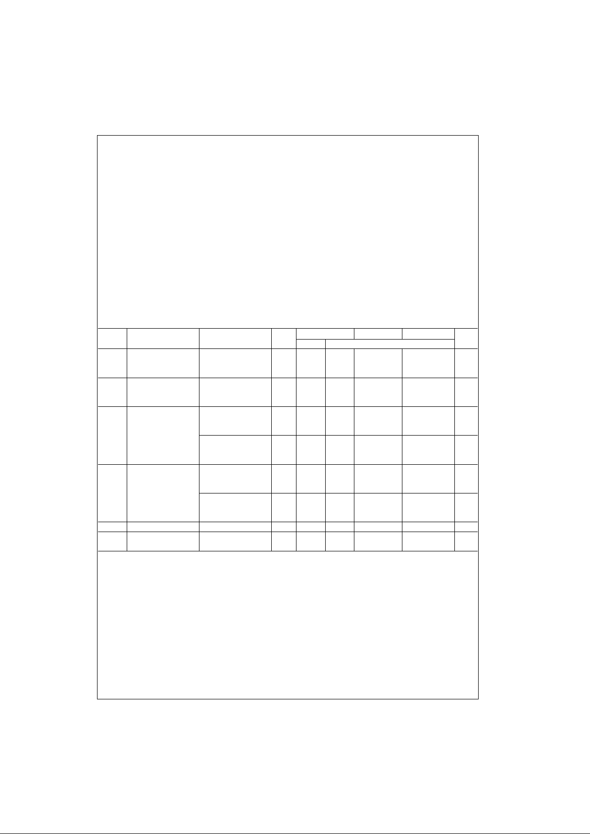
Absolute Maximum Ratings(Note 1)
(Note 2)
Recommended Operating
Conditions
Note 1: Maximum Ratings are those values beyond which damage to the
device may occur.
Note 2: Unless otherwise specified all voltages are referenced to ground.
Note 3: Power Dissipation te mperature d erating — pl astic “N” pa ckage: −
12 mW/°C from 65°C to 85°C.
DC Electrical Characteristics (Note 4)
Note 4: For a powe r supply o f 5V ±10% the worst case output voltages (VOH, and VOL) occur for HC at 4.5V. Thus the 4. 5V valu es shou ld be u sed when
designing with this supply. Worst case V
IH
and VIL occur at V
CC
= 5.5V and 4.5V respectively. (The VIH value at 5.5V is 3 .8 5V.) The worst c as e leakage cur-
rent (I
IN
, ICC, and IOZ) occur for CMOS at the higher voltage and so th e 6. 0V values should be use d.
Supply Voltage (VCC) −0.5 to +7.0V
DC Input Voltage (V
IN
) −1.5 to V
CC
+1.5V
DC Output Voltage (V
OUT
) −0.5 to V
CC
+0.5V
Clamp Diode Current (I
IK
, IOK) ±20 mA
DC Output Current, per pin (I
OUT
) ±25 mA
DC V
CC
or GND Current, per pin (ICC) ±50 mA
Storage Temperature Range (T
STG
) −65°C to +150°C
Power Dissipation (P
D
)
(Note 3) 600 mW
S.O. Package only 500 mW
Lead Temperature (T
L
)
(Solderi ng 10 seconds) 260°C
Min Max Units
Supply Voltage (V
CC
)26V
DC Input or Output Voltage 0 V
CC
V
(V
IN
, V
OUT
)
Operating Temperatur e Range (T
A
) −40 +85 °C
Input Rise or Fall Times
(t
r
, tf) V
CC
= 2.0V 1000 ns
V
CC
= 4.5V 500 ns
V
CC
= 6.0V 400 ns
Symbol Parameter Conditions
V
CC
TA = 25°CTA = −40 to 85°CTA = −55 to 125°C
Units
Typ Guaranteed Limits
V
IH
Minimum HIGH Level 2.0V 1.5 1.5 1.5
VInput Voltage 4.5V 3.15 3.15 3.15
6.0V 4.2 4.2 4.2
V
IL
Maximum LOW Level 2.0V 0.5 0.5 0.5
VInput Voltage 4.5V 1.35 1.35 1.35
6.0V 1.8 1.8 1.8
V
OH
Minimum HIGH Level V
IN
= VIH or V
IL
2.0V 2.0 1.9 1.9 1.9
Output Voltage |I
OUT
| ≤ 20 µA 4.5V 4.5 4.4 4.4 4.4 V
6.0V 6.0 5.9 5.9 5.9
V
IN
= VIH or V
IL
|I
OUT
| ≤ 4.0 mA 4.5V 4.2 3.98 3.84 3.7
V
|I
OUT
| ≤ 5.2 mA 6.0V 5.7 5.48 5.34 5.2
V
OL
Maximum LOW Level V
IN
= VIH or V
IL
2.0V 0 0.1 0.1 0.1
Output Voltage |I
OUT
| ≤ 20 µA 4.5V 0 0.1 0.1 0.1 V
6.0V 0 0.1 0.1 0.1
V
IN
= VIH or V
IL
|I
OUT
| ≤ 4.0 mA 4.5V 0.2 0.26 0.33 0.4
V
|I
OUT
| ≤ 5.2 mA 6.0V 0.2 0.26 0.33 0.4
I
IN
Maximum Input Current V
IN
= VCC or GND 6.0V ±0.1 ±1.0 ±1.0 µA
I
CC
Maximum Quiescent V
IN
= VCC or GND
6.0V 8.0 80 160 µA
Supply Current I
OUT
= 0 µA
Page 4

www.fairchildsemi.com 4
MM74HC4514
AC Electrical Characteristics
V
CC
= 5V, TA = 25°C, CL = 15 pF, tr = t
f
= 6 ns
AC Electrical Characteristics
V
CC
= 2.0V − 6.0V, CL = 50 pF, tr = t
f
= 6 ns (unless otherwise specified)
Note 5: CPD determines the no lo ad dynamic power con s um ption, PD = CPD V
CC
2
f + ICC VCC, and the no load dynam ic c urrent consumption ,
I
S
= CPDVCCf + ICC.
Symbol Parameter Conditions T yp
Guaranteed
Units
Limit
t
PHL
, t
PLH
Maximum Propagation Delay Data to Output 18 30 ns
t
PHL
Maximum Propagation Delay LE to Output 18 30 ns
t
PLH
Maximum Propagation Delay LE to Output 24 40 ns
t
PHL
Maximum Propagation Delay Inhibit to Output 16 30 ns
t
PLH
Maximum Propagation Delay Inhibit to Output 24 40 ns
t
s
Minimum Setup Time, Date to LE 20 ns
t
H
Minimum Hold Time, LE to Data 5ns
t
W
Minimum Pulse Width, Latch Enable 16 ns
Symbol Parameter Conditions
V
CC
TA = 25°CTA= −40 to 85°CTA = −55 to 125°C
Units
Typ Guaranteed Limits
t
PHL
, t
PLH
Maximum Propagation 2.0V 80 175 220 263
nsDelay Data to Output 4.5V 18 35 44 53
6.0V 16 30 38 45
t
PHL
Maximum Propagation 2.0V 80 175 220 263
nsDelay LE to Output 4.5V 19 35 44 53
6.0V 17 30 38 45
t
PLH
Maximum Propagation 2.0V 120 230 290 343
nsDelay LE to Output 4.5V 27 46 58 69
6.0V 22 39 49 58
t
PHL
Maximum Propagation 2.0V 70 175 220 263
nsDelay Inhibit to Output 4.5V 18 35 44 53
6.0V 16 30 38 45
t
PLH
Maximum Propagation 2.0V 120 230 290 343
nsDelay Inhibit to Output 4.5V 27 46 58 69
6.0V 22 39 49 58
t
s
Minimum Setup Time, 2.0V 100 125 150
nsData to LE 4.5V 20 25 30
6.0V 17 21 25
t
H
Minimum Hol d Time, 2.0V 5 5 5
nsLE to Data 4.5V 5 5 5
6.0V 5 5 5
t
W
Minimum Pulse Width, 2.0V 80 100 120
nsLatch Enable 4.5V 16 20 24
6.0V 14 17 20
C
PD
Power Dissipation
290 pF
Capacitance (Note 5)
C
IN
Maximum Input
510 10 10 pF
Capacitance
Page 5

5 www.fairchildsemi.com
MM74HC4514
Physical Dimensions inches (millimeters) unless otherwise noted
24-Lead Small Outline Integrated Circuit (SOIC), JEDEC MS-013, 0.300” Wide
Package Number M24B
Page 6

www.fairchildsemi.com 6
MM74HC4514
Physical Dimensions inches (millimeters) unless otherwise noted (Continued)
24-Lead Thin Shrink Small Outline Package (TSSOP), JEDEC MO-153, 4.4mm Wide
Package Number MTC24
Page 7

7 www.fairchildsemi.com
MM74HC4514 4-to-16 Line Decoder with Latch
Physical Dimensions inches (millimeters) unless otherwise noted (Continued)
24-Lead Plastic Dual-In-Line Package (PDIP), JEDEC MS-100, 0.300” Wide
Package Number N24C
Fairchild does not assume any responsibility for use of any circu itry described, no circuit patent license s are implied and
Fairchild reserves the right at any time without notice to change said circuitry and specifications.
LIFE SUPPORT POLICY
FAIRCHILD’S PRODUCTS ARE NOT AUTHORIZED FOR USE AS CRITICAL COMPONENTS IN LIFE SUPPORT
DEVICES OR SYSTEMS WITHOUT THE EXPRESS WRITTEN APPROVAL OF THE PRESIDENT OF FAIRCHILD
SEMICONDUCTOR CORPORATION. As used herein:
1. Life support devices or systems are devices or syste ms
which, (a) are intended for surgical implant into the
body, or (b) support or sustain life, and (c) whose failure
to perform when properly used in accordance with
instructions for use provided i n the labe li ng, can be re asonably expected to result in a significant injury to the
user.
2. A critical component in any compo nent o f a li fe supp ort
device or system whose failu re to perform can b e reasonably expected to c ause th e fa i lure of the li fe s upp or t
device or system, or to affect its safety or effectiveness.
www.fairchildsemi.com
 Loading...