

Datasheet MM74HC4316CW, MM74HC4316WMX, MM74HC4316SJ, MM74HC4316SJX, MM74HC4316WM Datasheet (Fairchild Semiconductor)
...Page 1
February 1984
Revised February 1999
MM74HC4316 Quad Analog Switch with Level Translator
© 1999 Fairchild Semiconductor Corporation DS005369.prf www.fairchildsemi.com
MM74HC4316
Quad Analog Switch with Level Translator
General Description
The MM74HC4316 device s are digitally controlled ana log
switches implemented in advanced silicon-gate CMOS
technology. These switches have low “ON” resistance and
low “OFF” leakages. They are bid irectional switc hes, thus
any analog input may be used as an output and vice-versa.
Three supply pin s are provided on the MM74 HC4316 to
implement a level translator which enables this circuit to
operate with 0–6V logic levels and up to ±6V analog switch
levels. Th e MM74H C43 16 als o has a com mon en able inpu t
in addition to each switch's control which when LOW will
disable all switches to their OFF state. All analog inputs
and outputs and digital inputs are protec ted from electrostatic damage by diodes to V
CC
and ground.
Features
■ Typical switch enable time: 20 ns
■ Wide analog input voltage range: ±6V
■ Low “ON” resistance:
50 typ. (V
CC−VEE
= 4.5V) 30 typ. (VCC−V
EE
= 9V)
■ Low quiescent current: 80 µA maximum (74HC)
■ Matched switch characteristics
■ Individual switch controls plus a common enable
Ordering Code:
Devices also availab le in Tape and Reel. Specify by appending th e s uffix let t er “X” to the ordering cod e.
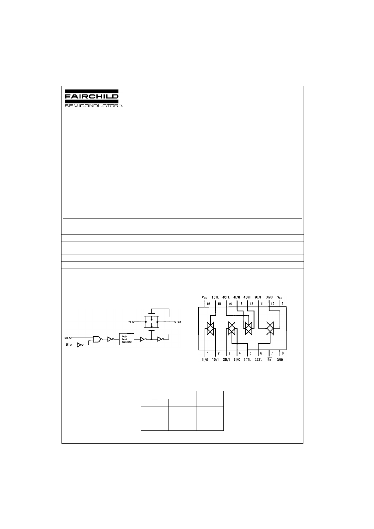
Logic Diagram Connection Diagram
Pin Assignments for DIP, SOIC, SOP and TSSOP
Top View
Truth Table
Order Number Package Number Package Description
MM74HC4316M M16A 16-Lead Small Outline Integrated Package (SOIC), JEDEC MS-012, 0.150” Narrow
MM74HC4316SJ M16D 16-Lead Small Outline Package (SOP), EIAJ TYPE II, 5.3mm Wide
MM74HC4316MTC MTC16 16-Lead Thin Shrink Small Outline Package (TSSOP), JEDEC MO-1536, 4.4mm Wide
MM74HC4316N N16E 16-Lead Plastic Dual-In-Line Package (PDIP), JEDEC MS-001, 0.300” Wide
Inputs Switch
En
CTL I/O–O/I
HX“OFF”
LL“OFF”
LH“ON”
Page 2
www.fairchildsemi.com 2
MM74HC4316
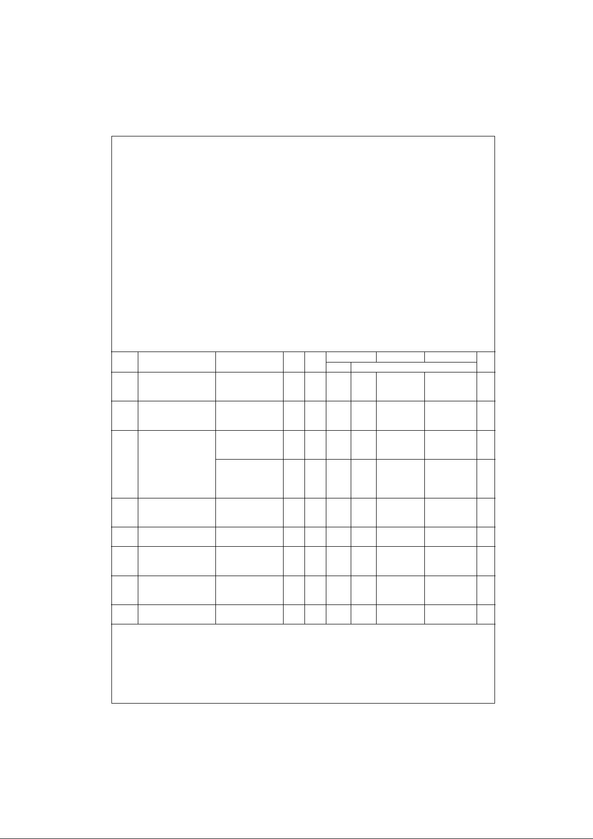
Absolute Maximum Ratings(Note 1)
(Note 2)
Recommended Operating
Conditions
Note 1: Absolute Maximum Ratings are those values beyond which dam-
age to the device may occur.
Note 2: Unless otherwise specified all voltages are referenced to ground.
Note 3: Power Dissipation temper ature dera ting — plas tic “N” packa ge: −
12 mW/°C from 65 °C to 85°C.
DC Electrical Characteristics (Note 4)
Note 4: For a power supp ly o f 5V ±10% the worst case on resistances (RON) occurs for HC a t 4.5V. Thus the 4.5V valu es s hou ld b e us ed w hen de signi ng
with this supply. Worst case V
IH
and VIL occur at VCC=5.5V and 4.5V res pec tivel y. (The VIH value at 5.5V is 3.85V.) The worst case leakage c urrent occurs
for CMOS at the higher voltage and so the 5. 5V values should be used.
Note 5: At supply voltag es (V
CC–VEE
) approaching 2V the analo g switch on resist ance becom es extr emely non- linear. Therefore it is recom mended that
these devices be us ed to transmit digital only w hen using these supply v oltages.
Supply Voltage (VCC) −0.5 to +7.5V
Supply Voltage (V
EE
) +0.5 to −7.5V
DC Control Input Voltage (V
IN
) −1.5 to V
CC
+1.5V
DC Switch I/O Voltage (V
IO
)V
EE
−0.5 to V
CC
+0.5V
Clamp Diode Current (I
IK
, IOK) ±20 mA
DC Output Current, per pin (I
OUT
) ±25 mA
DC V
CC
or GND Current, per pin (ICC) ±50 mA
Storage Temperature Range (T
STG
) −65°C to +150°C
Power Dissipation (P
D
)
(Note 3) 600 mW
S.O. Package only 500 mW
Lead Temperature (T
L
)
(Soldering 10 seconds) 260°C
Min Max Units
Supply Voltage (V
CC
)26V
Supply Voltage (V
EE
)0−6V
DC Input or Output Voltage
(V
IN
, V
OUT
)0V
CC
V
Operating Temperature Range (T
A
) −40 +85 °C
Input Rise or Fall Times
(t
r
, tf) VCC = 2.0V 1000 ns
V
CC
= 4.5V 500 ns
V
CC
= 6.0V 400 ns
V
CC
= 12.0V 250 ns
Symbol Parameter Conditions
VEEV
CC
TA = 25°CTA = −40 to 85°CTA = −55 to 125°C
Units
Typ Guaranteed Limits
V
IH
Minimum HIGH Level 2.0V 1.5 1.5 1.5 V
Input Voltage 4.5V 3.15 3.15 3.15 V
6.0V 4.2 4.2 4.2 V
V
IL
Maximum LOW Level 2.0V 0.5 0.5 0.5 V
Input Voltage 4.5V 1.35 1.35 1.35 V
6.0V 1.8 1.8 1.8 V
R
ON
Minimum “ON” Resistance V
CTL
= VIH, IS = 2.0 mA GND 4.5V 100 170 200 220 Ω
(Note 5) V
IS
= VCC to V
EE
−4.5V 4.5V 40 85 105 110 Ω
(Figure 1) −6.0V 6.0V 30 70 85 90 Ω
GND 2.0V 100 180 215 240 Ω
V
CTL
= VIH, IS = 2.0 mA GND 4.5V 40 80 100 120 Ω
V
IS
= VCC or V
EE
−4.5V 4.5V 50 60 75 80 Ω
(Figure 1) −6.0V 6.0V 20 40 60 70 Ω
R
ON
Maximum “ON” Resistance V
CTL
= V
IH
GND 4.5V 10 15 20 20 Ω
Matching V
IS
= VCC to V
EE
−4.5V 4.5V 5 10 15 15 Ω
−6.0V 6.0V 5 10 15 15 Ω
I
IN
Maximum Control V
IN
= VCC or GND GND 6.0V ±0.1 ±1.0 ±1.0 µA
Input Current
I
IZ
Maximum Switch “OFF” V
OS
= VCC or V
EE
GND 6.0V ±60 ±600 ±600 nA
Leakage Current V
IS
= VEE or V
CC
−6.0V 6.0V ±100 ±1000 ±1000 nA
V
CTL
= VIL (Figure 2)
I
IZ
Maximum Switch “ON” V
IS
= VCC to V
EE
GND 6.0V ±40 ±150 ±150 nA
Leakage Current V
CTL
= VIH, VOS = OPEN −6.0V 6.0V ±60 ±300 ±300 nA
(Figure 3)
I
CC
Maximum Quiescent V
IN
= VCC or GND GND 6.0V 2.0 20 40 µA
Supply Current I
OUT
= 0 µA −6.0V 6.0V 8.0 80 160 µA
Page 3
3 www.fairchildsemi.com
MM74HC4316
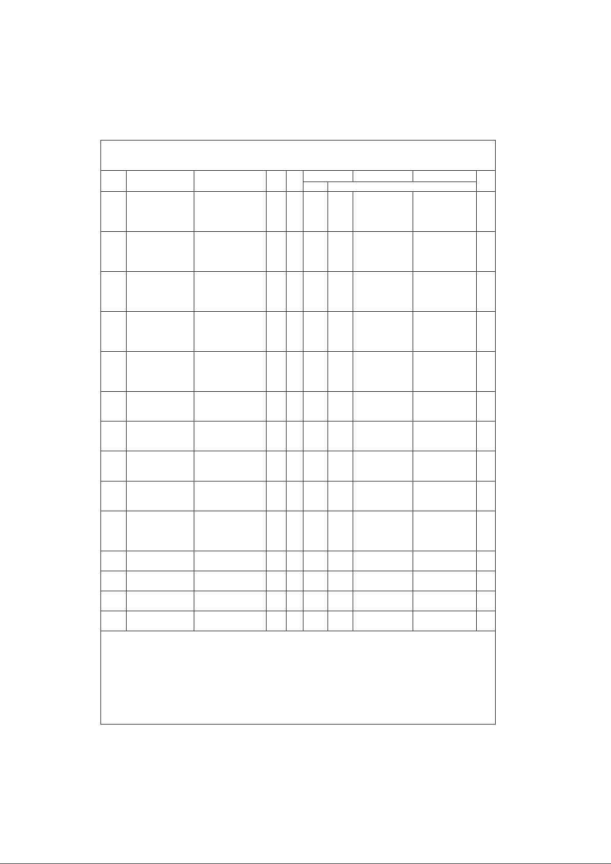
AC Electrical Characteristics
VCC = 2.0V−6.0V, VEE = 0V−6V, CL = 50 pF (unless otherwise specified)
Note 6: Adjust 0 dBm for F = 1 KHz (Null RL/Ron Attenuation).
Note 7: V
IS
is centered at VCC–VEE/2.
Note 8: Adjust for 0 dBm.
Symbol Parameter Conditions
VEEV
CC
TA = +25°CTA = −40°C to +85°CTA = −55°C to +125°C
Units
Typ Guaranteed Limits
t
PHL
, Maximum Propagation GND 2.0V 25 50 63 75 ns
t
PLH
Delay Switch GND 4.5V 5 10 13 15 ns
In to Out −4.5V 4.5V 4 8 12 14 ns
−6.0V 6.0V 3 7 11 13 ns
t
PZL
, Maximum Switch RL = 1 kΩ GND 2.0V 30 165 206 250 ns
t
PZH
Turn “ON” Delay GND 4.5V 20 35 43 53 ns
(Control) −4.5V 4.5V 15 32 39 48 ns
−6.0V 6.0V 14 30 37 45 ns
t
PHZ
, Maximum Switch RL = 1 kΩ GND 2.0V 45 250 312 375 ns
t
PLZ
Turn “OFF” Delay GND 4.5V 25 50 63 75 ns
(Control) −4.5V 4.5V 20 44 55 66 ns
−6.0V 6.0V 20 44 55 66
t
PZL
, Maximum Switch GND 2.0V 35 205 256 308 ns
t
PZH
Turn “ON” Delay GND 4.5V 20 41 52 62 ns
(Enable) −4.5V 4.5V 19 38 48 57 ns
−6.0V 6.0V 18 36 45 54 ns
t
PLZ
, Maximum Switch GND 2.0V 58 265 330 400 ns
t
PHZ
Turn “OFF” Delay GND 4.5V 28 53 67 79 ns
(Enable) −4.5V 4.5V 23 47 59 70 ns
−6.0V 6.0V 21 47 59 70 ns
f
MAX
Minimum Frequency RL = 600Ω, VIS = 2V
PP
0V 4.5 40 MHz
Response (Figure 7) at (VCC−VEE/2) −4.5V 4.5V 100 MHz
20 log (VOS/VIS)= −3 dB (Note 6) (Note 7)
Control to Switch RL = 600Ω, F = 1 MHz 0V 4.5V 100 mV
Feedthrough Noise CL = 50 pF −4.5V 4.5V 250 mV
(Figure 8) (Note 7) (Note 8)
Crosstalk Between RL = 600Ω, F = 1 MHz
any Two Switches 0V 4.5V −52 dB
(Figure 9) −4.5V 4.5V −50 dB
Switch OFF Signal RL = 600Ω, F = 1 MHz
Feedthrough Isolation V
CTL
= VIL,0V4.5V−42 dB
(Figure 10) (Note 7) (Note 8) −4.5V 4.5V −44 dB
THD Sinewave Harmonic RL = 10 KΩ, CL = 50 pF,
Distortion F = 1 KHz
(Figure 11) VIS = 4VPP0V 4.5V 0.013 %
VIS = 8VPP−4.5V 4.5V 0.008 %
C
IN
Maximum Control 5 pF
Input Capacitance
C
IN
Maximum Switch 35 pF
Input Capacitance
C
IN
Maximum Feedthrough V
CTL
= GND 0.5 pF
Capacitance
C
PD
Power Dissipation 15 pF
Capacitance
Page 4

www.fairchildsemi.com 4
MM74HC4316
AC Test Circuits and Switching Time Waveforms
FIGURE 1. “ON” Resistance FIGURE 2. “OFF” Channel Leakage Current
FIGURE 3. “ON” Channel Leakage Current
FIGURE 4. t
PHL
, t
PLH
Propagation Delay Time Signal Input to Signal Output
FIGURE 5. t
PZL
, t
PLZ
Propagation Delay Time Control to Signal Output
FIGURE 6. t
PZH
, t
PHZ
Propagation Delay Time Control to Signal Output
Page 5

5 www.fairchildsemi.com
MM74HC4316
AC Test Circuits and Switching Time Waveforms (Continued)
FIGURE 7. Frequenc y Re sp on se
FIGURE 8. Crosstalk: Control Input to Signal Output
FIGURE 9. : Crosstalk Between Any Two Switches
FIGURE 10. Switch OFF Signal Feedthrough Isolation FIGURE 11. Sinewave Distortion
Page 6

www.fairchildsemi.com 6
MM74HC4316
Typical Performance Characteristics
Typical “ON” Resistance Typical Crosstalk Between
Any Two Switches
Typical Frequency Response
Special Considerations
In certain applications the external load-resistor current
may include both V
CC
and signal line components. To
avoid drawing V
CC
current when switch current f lows into
the analog switch input pins, the voltage drop across the
switch must not exceed 0.6V (calculated from the ON resistance).
Page 7

7 www.fairchildsemi.com
MM74HC4316
Physical Dimensions inches (millimeters) unless otherwise noted
16-Lead Small Outline Integrated Circuit (SOIC), JEDEC MS-012, 0.150” Narrow
Package Number M16A
16-Lead small Outline Package (SOP), EIAJ TYPE II, 5.3mm Wide
Package Number M16D
Page 8

www.fairchildsemi.com 8
MM74HC4316
Physical Dimensions inches (millimeters) unless otherwise noted (Continued)
16-Lead Thin Shrink Small Outline Package (TSSOP), JEDEC MO-153, 4.4mm Wide
Package Number MTC16
Page 9

Fairchild does not assume any responsibility for use of any circuitry described, no circuit patent licenses are implied and Fairchild reserves the right at any time without notice to change said circuitry and specifications.
MM74HC4316 Quad Analog Switch with Level Translator
LIFE SUPPORT POLICY
FAIRCHILD’S PRODUCTS ARE NOT AUTHORIZED FOR USE AS CRITICAL COMPONENTS IN LIFE SUPPORT
DEVICES OR SYSTEMS WITHOUT THE EXPRESS WRITTEN APPROVAL OF THE PRESIDENT OF FAIRCHILD
SEMICONDUCTOR CORPORATION. As used herein:
1. Life support de vices o r syst ems are devices or systems
which, (a) are intended for surgical implant into the
body, or (b) support or sustain life, and (c) whose failure
to perform when properly used in accordance with
instructions for use provided i n the labe li ng, can be re asonably expected to result in a significant injury to the
user.
2. A critica l compo nent i n any compo nent o f a life s uppor t
device or system whose failu re to perform can b e reasonably expected to c ause th e fa i lure of the li fe s upp or t
device or system, or to affect its safety or effectiveness.
www.fairchildsemi.com
Physical Dimensions inches (millimeters) unless otherwise noted (Continued)
16-Lead Plastic Dual-In-Line Package (PDIP), JEDEC MS-001, 0.300” Wide
Package Number N16E
 Loading...