

Datasheet MM74HC4053MTCX, MM74HC4053MX, MM74HC4053M, MM74HC4053SJX, MM74HC4053WM Datasheet (Fairchild Semiconductor)
...Page 1
MM74HC4051 • MM74HC4052 • MM74HC4053
8-Channel Analog Multiplexer •
Dual 4-Channel Analog Multiplexer •
Triple 2-Channel Analog Multiplexer
MM74HC4051 • MM74HC4052 • MM74HC4053 8-Channel Analog Multiplexer •
August 1984
Revised May 1999
General Description
The MM74HC4051, MM74HC4052 and MM74HC4053
multiplexers are digitally controlled analog switches implemented in advanced silicon-gate CMOS technology. These
switches have low “on” resista nce and low “off” leakages.
They are bidirectional switches, thus any analog inp ut m ay
be used as an output and vice-versa. Also these switches
contain linearization circuitry which lowers the on resistance and increases switch linearity. These devices allow
control of up to ±6V (peak) ana log signals wi th digital control signals of 0 to 6V. Three supply pins are provided for
, ground, and VEE. This enables the connection of 0–
V
CC
5V logic signals when V
of ±5V when V
inhibit control which when HIGH will disable all switches to
their off state. All analog inputs and outputs and digital
inputs are protected from electrostatic dama ge by diodes
to V
CC
MM74HC4051: This device connects to gether the outp uts
of 8 switches, thus achieving an 8 channel Multiplexer. The
binary code placed on the A , B, and C select lines dete rmines which one o f the eight switches is “on”, and connects one of the eight inputs to the common output.
EE
and ground.
= 5V and an analog input range
CC
= 5V. All three devices also have an
MM74HC4052: This d evice connects t ogether the output s
of 4 switches in two sets, thus achieving a pair of 4-channel
multiplexers. The binary code placed on the A, and B
select lines determine which switch in each 4 channel section is “on”, connecting one of the four inputs in each section to its common output. This enables the implementation
of a 4-channel differential multiplexer.
MM74HC4053: This device contains 6 switches whose outputs are connected together in pairs, thus implementing a
triple 2 channel mult iplexer, or the equivalent of 3 singl epole-double throw con figurations. Each of the A, B, or C
select lines independently controls one pair of switches,
selecting one of the two switches to be “on”.
Features
■ Wide analog input voltage range: ±6V
■ Low “on” resistance:
CC–VEE
CC–VEE
= 4.5V)
= 9V)
50 typ. (V
30 typ. (V
■ Logic level translat ion to enabl e 5V logi c with ±5V ana-
log signals
■ Low quiescent current: 80 µA maximum (74HC)
■ Matched Switch characteristic
Ordering Code:
Order Number Package Number Package Description
MM74HC4051M M16A 16-Lead Small Outline Integrated Circuit (SOIC), JEDEC MS-012, 0.150” Narrow
MM74HC4051WM M16B 16-Lead Small Outline Integrated Circuit (SOIC), JEDEC MS-013, 0.300” Wide
MM74HC4051SJ M16D 16-Lead Small Outline Package (SOP), EIAJ TYPE II, 5.3mm Wide
MM74HC4051MTC MTC16 16-Lead Thin Shrink Small Outline Package (TSSOP), JEDEC MO-153, 4.4mm Wide
MM74HC4051N N16E 16-Lead Plastic Dual-In-Line Package (PDIP), JEDEC MS-0010.300” Wide
MM74HC4052M M16A 16-Lead Small Outline Integrated Circuit (SOIC), JEDEC MS-012, 0.150” Narrow
MM74HC4052WM M16B 16-Lead Small Outline Integrated Circuit (SOIC), JEDEC MS-013, 0.300” Wide
MM74HC4052SJ M16D 16-Lead Small Outline Package (SOP), EIAJ TYPE II, 5.3mm Wide
MM74HC4052MTC MTC16 16-Lead Thin Shrink Small Outline Package (TSSOP), JEDEC MO-153, 4.4mm Wide
MM74HC4052N N16E 16-Lead Plastic Dual-In-Line Package (PDIP), JEDEC MS-0010.300” Wide
MM74HC4053M M16A 16-Lead Small Outline Integrated Circuit (SOIC), JEDEC MS-012, 0.150” Narrow
MM74HC4053WM M16B 16-Lead Small Outline Integrated Circuit (SOIC), JEDEC MS-013, 0.300” Wide
MM74HC4053SJ M16D 16-Lead Small Outline Package (SOP), EIAJ TYPE II, 5.3mm Wide
MM74HC4053MTC MTC16 16-Lead Thin Shrink Small Outline Package (TSSOP), JEDEC MO-153, 4.4mm Wide
MM74HC4053N N16E 16-Lead Plastic Dual-In-Line Package (PDIP), JEDEC MS-0010.300” Wide
Devices also availab le in Tape and Reel. Specify by appending th e s uffix let t er “X” to the ordering code.
© 1999 Fairchild Semiconductor Corporation DS005353.prf www.fairchildsemi.com
Page 2
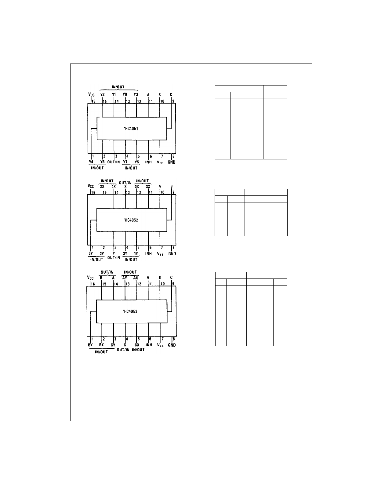
Connection Diagrams
Pin Assignments for DIP, SOIC, SO P and TSSOP
Top View
MM74HC4051 • MM74HC4052 • MM74HC4053
Truth T ables
MM744051
Input “ON”
InhCBAChannel
H XXX None
L LLL Y0
LLLH Y1
LLHL Y2
LLHH Y3
LHLL Y4
LHLH Y5
LHHL Y6
L HHH Y7
MM744052
Inputs “ON” Channels
Inh B A X Y
H X X None None
LLL 0X 0Y
LLH 1X 1Y
LHL 2X 2Y
LHH 3X 3Y
Top View
Top View
www.fairchildsemi.com 2
MM744053
Input “ON” Channels
InhCBA C b a
H X X X None None None
L L L L CX BX AX
LLLHCX BX AY
L L H L CX BY AX
LLHHCX BY AY
L H L L CY BX AX
LHLHCY BX AY
L H H L CY BY AX
L HHH CY BY AY
Page 3
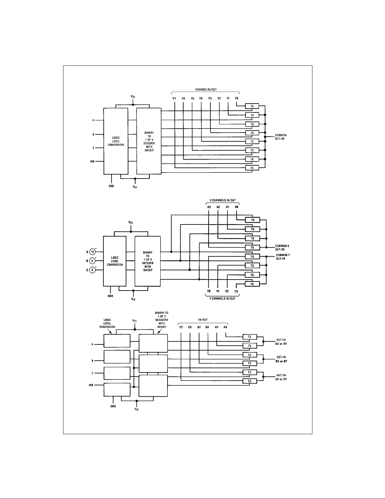
Logic Diagrams
MM74HC4051 • MM74HC4052 • MM74HC4053
MM74HC4051
MM74HC4052
MM74HC4053
3 www.fairchildsemi.com
Page 4
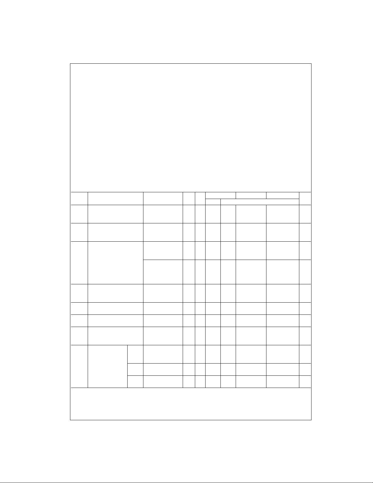
Absolute Maximum Ratings(Note 1)
(Note 2)
Supply Voltage (V
Supply Voltage (V
Control Input Voltage (V
Switch I/O Voltage (V
Clamp Diode Current (I
Output Current, per pin (I
or GND Current, per pin (ICC) ±50 mA
V
CC
Storage Temperature Range (T
Power Dissipation (P
) −0.5 to +7.5V
CC
) +0.5 to −7.5V
EE
) −1.5 to V
IN
)V
IO
, IOK) ±20 mA
IK
) ±25 mA
OUT
STG
)
D
−0.5 to V
EE
) −65°C to +150°C
(Note 3) 600 mW
S.O. Package only 500 mW
Lead Temperature (T
)
L
(Soldering 10 seconds) 260°C
DC Electrical Characteristics (Note 4)
Symbol Parameter Conditions
MM74HC4051 • MM74HC4052 • MM74HC4053
V
Minimum HIGH Level 2.0V 1.5 1.5 1.5 V
IH
Input Voltage 4.5V 3.15 3.15 3.15 V
V
Maximum LOW Level 2.0V 0.5 0.5 0.5 V
IL
Input Voltage 4.5V 1.35 1.35 1.35 V
R
Maximum “ON” Resistance V
ON
(Note 5) V
R
Maximum “ON” Resistance V
ON
Matching V
I
Maximum Control V
IN
Input Current V
I
Maximum Quiescent V
CC
Supply Current I
I
Maximum Switch “OFF” V
IZ
Leakage Current V
(Switch Input) V
I
Maximum Switch V
IZ
“ON” Leakage HC4051 V
Current (Figure 3)
HC4052 V
HC4053 V
= VIL, IS = 2.0 mA GND 4.5V 40 160 200 240 Ω
INH
= VCC to V
IS
(Figure 1) −6.0V 6.0V 20 100 125 140 Ω
V
= VIL, IS = 2.0 mA GND 2.0V 100 230 280 320 Ω
INH
V
= VCC or V
IS
(Figure 1) −4.5V 4.5V 20 90 120 140 Ω
= V
CTL
IL
= VCC to GND −4.5V 4.5V 5 10 15 15 Ω
IS
= VCCor GND ±0.1 ±1.0 ±1.0 µA
IN
= 2−6V
CC
= VCC or GND GND 6.0V 8 80 160 µA
IN
= 0 µA −6.0V 6.0V 16 160 320 µA
OUT
= VCCor V
OS
= VEEor V
IS
= VIH (Figure 2)
INH
= VCC to V
IS
= V
INH
IL
V
= VCC to V
IS
= V
(Figure 3) −6.0V 6.0V ±0.2 ±2.0 ±2.0 µA
INH
IL
V
= VCC to V
IS
= VIL (Figure 3) −6.0V 6.0V ±0.1 ±1.0 ±1.0 µA
INH
Recommended Operating
Conditions
Min Max Units
Supply Voltage (V
+1.5V
CC
CC
Supply Voltage (V
+0.5V
DC Input or Output Voltage
, V
(V
IN
OUT
Operating Temperature Range (T
Input Rise or Fall Times
, tf) VCC = 2.0V 1000 ns
(t
r
V
CC
V
Note 1: Absolute Maximum Ratings are those values beyond which damage to the device may occur.
Note 2: Unless otherwise specified all voltages are referenced to ground.
Note 3: Power Dissipation tem perature de rating — pla stic “N” pac kage: −
12 mW/°C from 65 °C to 85°C.
VEEV
−4.5V 4.5V 30 120 150 170 Ω
EE
GND 4.5V 40 110 140 170 Ω
EE
−6.0V 6.0V 15 80 100 115 Ω
GND 4.5V 10 20 25 25 Ω
−6.0V 6.0V 5 10 12 15 Ω
GND 6.0V ±60 ±600 ±600 nA
EE
−6.0V 6.0V ±100 ±1000 ±1000 nA
CC
GND 6.0V ±0.2 ±2.0 ±2.0 µA
EE
−6.0V 6.0V ±0.4 ±4.0 ±4.0 µA
GND 6.0V ±0.1 ±1.0 ±1.0 µA
EE
GND 6.0V ±0.1 ±1.0 ±1.0 µA
EE
CC
TA = 25°CTA = −40 to 85°CTA = −55 to 125°C
CC
Typ Guaranteed Limits
6.0V 4.2 4.2 4.2 V
6.0V 1.8 1.8 1.8 V
)26V
CC
)0−6V
EE
)0V
) −40 +85 °C
A
= 4.5V 500 ns
= 6.0V 400 ns
CC
V
Units
www.fairchildsemi.com 4
Page 5

DC Electrical Characteristics (Continued)
MM74HC4051 • MM74HC4052 • MM74HC4053
Symbol Parameter Conditions
I
Maximum Switch V
IZ
“OFF” Leakage HC4051 V
Current (Common Pin) V
HC4052 V
HC4053 V
Note 4: For a power sup ply o f 5V ±10% the worst case on resistances (RON) occurs for HC at 4.5 V. Thus the 4.5V val ues shou ld be us ed w hen de sign ing
with this supply. Worst case V
for CMOS at the higher v oltage and so the 5.5V v alues should be used.
Note 5: At supply voltages (V
these devices be use d t o tr ansmit digital only when using these supply voltages.
and VIL occur at V
IH
) approaching 2V the anal og switc h on resist ance beco mes ext remely non -linear. Therefore it is reco mmende d that
CC–VEE
= VCC or V
OS
= VEE or V
IS
= V
INH
IH
V
= VCC or V
OS
= VEE or V
IS
V
= V
INH
IH
V
= VCC or V
OS
= VEE or V
IS
V
= V
INH
IH
= 5.5V and 4. 5V respectively. (The VIH value at 5.5V is 3.85V.) The worst c as e leakage current occur
CC
VEEV
GND 6.0V ±0.2 ±2.0 ±2.0 µA
EE
−6.0V 6.0V ±0.4 ±4.0 ±4.0 µA
CC
GND 6.0V ±0.1 ±1.0 ±1.0 µA
EE
−6.0V 6.0V ±0.2 ±2.0 ±2.0 µA
CC
GND 6.0V ±0.1 ±1.0 ±1.0 µA
EE
−6.0V 6.0V ±0.1 ±1.0 ±1.0 µA
CC
TA = 25°CTA = −40 to 85°CTA = −55 to 125°C
CC
Typ Guaranteed Limits
AC Electrical Characteristics
V
= 2.0V−6.0V, V
CC
Symbol Parameter Conditions
t
, t
Maximum Propagation GND 2.0V 25 60 75 90 ns
PHL
PLH
Delay Switch In to Out GND 4.5V 5 12 15 18 ns
t
, t
Maximum Switch Turn RL = 1 kΩ GND 2.0V 92 355 435 515 ns
PZL
PZH
“ON” Delay GND 4.5V 69 87 103 ns
t
, t
Maximum Switch Turn GND 2.0V 65 290 365 435 ns
PHZ
PLZ
“OFF” Delay GND 4.5V 28 58 73 87 ns
f
Minimum Sw itch GND 4.5V 30 MHz
MAX
Frequency Response −4.5V 4.5V 35 MHz
20 log (VI/VO) = 3 dB
Control to Switch RL = 600Ω,VIS = 4 VPP0V 4.5V 1080 mV
Feedthrough Noise f = 1 MHz, VIS = 8 VPP−4.5V 4.5V 250 mV
Crosstalk between RL = 600Ω,VIS = 4 VPP0V 4.5 −52 dB
any Two Switches f = 1 MHz V
Switch OFF Signal RL = 600Ω,V
Feedthrough f = 1 MHz, V
Isolation V
THD Sinewave Harmonic RL = 10 kΩ,V
Distortion CL = 50 pF, V
C
Maximum Control 5 10 10 10 pF
IN
Input Capacitance
C
Maximum Switch Input 15 pF
IN
Input Capacitance 4051 Common 90
C
Maximum Feedthrough
IN
Capacitance
= 0V−6V, C
EE
= 50 pF (unless otherwise specified)
L
VEEV
CC
−4.5V 4.5V 4 8 12 14 ns
−6.0V 6.0V 3 7 11 13 ns
−4.5V 4.5V 16 46 58 69 ns
−6.0V 6.0V 15 41 51 62 ns
−4.5V 4.5V 18 37 46 56 ns
−6.0V 6.0V 16 32 41 48 ns
CL = 50 pF
= 8 VPP−4.5V 4.5V −50 dB
IS
= 4 VPP0V 4.5V −42 dB
IS
= 8 VPP−4.5V 4.5V −44 dB
IS
= V
CTL
IL
= 4 VPP0V 4.5V 0.013 %
IS
= 8 VPP−4.5V 4.5V 0.008 %
IS
f = 1 kHz
4052 Common 45
4053 Common 30
TA = 25°CTA = −40 to 85°CTA = −55 to 125°C
Typ Guaranteed Limits
5pF
Units
Units
5 www.fairchildsemi.com
Page 6

AC Test Circuits and Switching Time Waveforms
MM74HC4051 • MM74HC4052 • MM74HC4053
FIGURE 1. “ON” Resistance
FIGURE 3. “ON” Channel Leakage Current
FIGURE 4. t
FIGURE 5. t
PHL, tPLH
PZL, tPLZ
FIGURE 2. “OFF” Channel Leakage Current
Propagation Delay Time Signal Input to Signal Output
Propagation Delay Time Control to Signal Output
FIGURE 6. t
www.fairchildsemi.com 6
Propagation Delay Time Control to Signal Output
PZH, tPHZ
Page 7

AC Test Circuits and Switching Time Wavef orms (Continued)
FIGURE 7. Crosstalk: Control Input to Signal Output
MM74HC4051 • MM74HC4052 • MM74HC4053
FIGURE 8. Crosstalk Between Any Two Switches
Typical Performance Characteristics
Typical “On” Resistance vs Input Voltage
=−V
V
CC
EE
Special Considerations
In certain applications the external load-resistor current
may include both V
and signal line components. To
CC
avoid drawing V
the analog switch pins, th e voltage drop a cross t he switch
must not exceed 1.2V (calculated from the ON resistance).
7 www.fairchildsemi.com
current when switch current flows into
CC
Page 8

Physical Dimensions inches (millimeters) unless otherwise noted
MM74HC4051 • MM74HC4052 • MM74HC4053
16-Lead Small Outline Integrated Circuit (SOIC), JEDEC MS-012, 0.150” Narrow
16-Lead Small Outline Integrated Circuit (SOIC), JEDEC MS-013, 0.300” Wide
Package Number M16A
Package Number M16B
www.fairchildsemi.com 8
Page 9

Physical Dimensions inches (millimeters) unless otherwise noted (Continued)
MM74HC4051 • MM74HC4052 • MM74HC4053
16-Lead Small Outline Package (SOP), EIAJ TYPE II, 5.3mm Wide
Package Number M16D
9 www.fairchildsemi.com
Page 10

Physical Dimensions inches (millimeters) unless otherwise noted (Continued)
MM74HC4051 • MM74HC4052 • MM74HC4053
16-Lead Thin Shrink Small Outline Package (TSSOP), JEDEC MO-153, 4.4mm Wide
www.fairchildsemi.com 10
Package Number MTC16
Page 11

Physical Dimensions inches (millimeters) unless otherwise noted (Continued)
MM74HC4051 • MM74HC4052 • MM74HC4053 8-Channel Analog Multiplexer •
16-Lead Plastic Dual-In-Line Package (PDIP), JEDEC MS-001, 0.300” Wide
LIFE SUPPORT POLICY
FAIRCHILD’S PRODUCTS ARE NOT AUTHORIZED FOR USE AS CRITICAL COMPONENTS IN LIFE SUPPORT
DEVICES OR SYSTEMS WITHOUT THE EXPRESS WRITTEN APPROVAL OF THE PRESIDENT OF FAIRCHILD
SEMICONDUCTOR CORPORATION. As used herein:
1. Life sup por t de vices o r syst ems are dev ic es or syste ms
which, (a) are intended for surgical implant into the
body, or (b) support or sustain life, and (c) whose failure
to perform when properly used in accordance with
instructions for use provide d in the labe l ing, can be re asonably expected to result in a significant injury to the
user.
Package Number N16E
2. A c ritica l com ponent i n any compo nent o f a life s upp ort
device or system whose failu re to perform can b e reasonably expected to cause the failure of the life support
device or system, or to affect its safety or effectiveness.
www.fairchildsemi.com
Fairchild does not assume any responsibility for use of any circuitry described, no circuit patent licenses are implied and Fairchild reserves the right at any time without notice to change said circuitry and specifications.
 Loading...