

Datasheet MM74HC4046N, MM74HC4046SJ, MM74HC4046SJX, MM74HC4046MTCX, MM74HC4046M Datasheet (Fairchild Semiconductor)
...Page 1
February 1984
Revised February 1999
MM74HC4046 CMOS Phase Lock Loop
© 1999 Fairchild Semiconductor Corporation DS005352.prf www.fairchildsemi.com
MM74HC4046
CMOS Phase Lock Loop
General Description
The MM74HC4046 is a low power phase lock loop utilizing
advanced silicon-gate CMOS technology to obtain high frequency operation bot h in the phase com parator and VCO
sections. This device contai ns a low power linear voltage
controlled oscillator (VCO), a source follower, and three
phase comparators. The thre e phase comparators ha ve a
common signal input and a common comparator input. The
signal input has a self biasing ampli fier allowing sign als to
be either capacitively co upled to the phase comparators
with a small signal or direc tly coupled with standard inp ut
logic levels. This device is similar to the CD 4046 except
that the Zener diode of the metal gate CM OS device has
been replaced with a third phase comparator.
Phase Comparator I is an exclusive OR (XOR) gate. It provides a digital error signal that maintai ns a 90 phase shift
between the VCO’s center freque ncy and the input signal
(50% duty cycle input waveforms). This ph ase detector is
more susceptible to locking onto harmonics of the input frequency than phase comparator I, but pr ovi de s bet ter n oi se
rejection.
Phase comparator III is an S R fli p -flop ga te. It can b e used
to provide the phase co mp ara tor fun cti on s an d is similar to
the first comparator in performance.
Phase comparator II is an edge se nsitive digit al seque ntial
network. Two signal outputs are provided, a comparator
output and a phase pulse output. The comparator output is
a 3-STA TE output that provides a signal that locks the VCO
output signal to the i n pu t sign al with 0 phase shift b etween
them. This comparator is more susceptible to noise throwing the loop out of lock, but is less likely to lock onto h armonics than the other two comparators.
In a typical application a ny one of the three comparator s
feed an external filter network which in tur n f eed s th e VCO
input. This input is a very high impedance CMOS input
which also drives the source follower. The VCO’s operating
frequency is set by three external components co nnected
to the C1A, C1B, R1 and R2 pins. An inhibit pin is provided
to disable the VCO and the source follower, providing a
method of putting the IC in a low power state.
The source follower is a MOS transistor whose gate is connected to the VCO input and whose drain connects the
Demodulator output. This output normally i s used by tying
a resistor from pin 10 to ground , and provi des a means o f
looking at the VCO input without loading down modifying
the characteristics of the PLL filter.
Features
■ Low dynamic power consumption: (V
CC
= 4.5V)
■ Maximum VCO operating frequency:
12 MHz (V
CC
= 4.5V)
■ Fast comparator response time (V
CC
= 4.5V)
Comparator I: 25 ns
Comparator II: 30 ns
Comparator III: 25 ns
■ VCO has high linearity and high temperature stability
Ordering Code:
Devices also availab le in Tape and Reel. Specify by appending th e s uffix let t er “X” to the ordering cod e.
Order Number Package Number Package Description
MM74HC4046M M16A 16-Lead Small Outline Integrated Circuit (SOIC), JEDEC MS-012, 0.150” Narrow
MM74HC4046SJ M16D 16-Lead Small Outline Package (SOP), EIAJ TYPE II, 5.3mm Wide
MM74HC4046MTC MTC16 16-Lead Thin Shrink Small Outline Package (TSSOP), JEDEC MO-153, 4.4mm Wide
MM74HC4046N N16E 16-Lead Plastic Dual-In-Line Package (PDIP), JEDEC MS-001, 0.300” Wide
Page 2
www.fairchildsemi.com 2
MM74HC4046
Connection Diagram
Pin Assignments for DIP, SOIC, SOP and TSSOP
Block Diagram
Page 3
3 www.fairchildsemi.com
MM74HC4046
Absolute Maximum Ratings(Note 1)
(Note 2)
Recommended Operating
Conditions
Note 1: Maximum Ratings are those values beyond which damage to the
device may occur.
Note 2: Unless otherwise specified all voltages are referenced to ground.
Note 3: Power Dissipation te mperature d erating — pl astic “N” pa ckage: −
12 mW/°C from 65°C to 85°C.
DC Electrical Characteristics (Note 4)
Note 4: For a powe r supply o f 5V ±10% the worst case output voltages (VOH, and VOL) occur for HC at 4.5V. Thus the 4. 5V valu es shou ld be u sed when
designing with this supply. Worst case V
IH
and VIL occur at V
CC
= 5.5V and 4.5V respectively. (The VIH value at 5.5V is 3 .8 5V.) The worst c as e leakage cur-
rent (I
IN
, ICC, and IOZ) occur for CMOS at the higher voltage and so th e 6. 0V values should be used.
Supply Voltage (VCC) −0.5 to + 7.0V
DC Input Voltage (V
IN
) −1.5 to VCC +1.5V
DC Output Voltage (V
OUT
) −0.5 to VCC + 0.5V
Clamp Diode Current (I
IK
, IOK) ±20 mA
DC Output Current per pin (I
OUT
) ±25 mA
DC V
CC
or GND Current, per pin (ICC) ±50 mA
Storage Temperature Range (T
STG
) −65°C +150°C
Power Dissipation (P
D
)
(Note 3) 600 mW
S.O. Package only 500 mW
Lead Temperature (T
L
)
(Solderi ng 10 seconds) 260°C
Min Max Units
Supply Voltage (V
CC
)26V
DC Input or Output Voltage
(V
IN
, V
OUT
)0V
CC
V
Operating Temperature Range (T
A
) −40 +85 °C
Input Rise or Fall Times
(t
r
, tf) V
CC
= 2.0V 1000 ns
V
CC
= 4.5V 500 ns
V
CC
= 6.0V 400 ns
Symbol Parameter Conditions
V
CC
TA = 25°CTA = −40 to 85°CTA = −55 to 125°C
Units
Typ Guaranteed Limits
V
IH
Minimum HIGH Level 2.0V 1.5 1.5 1.5 V
Input Voltage 4.5V 3.15 3.15 3.15 V
6.0V 4.2 4.2 4.2 V
V
IL
Maximum LOW Level 2.0V 0.5 0.5 0.5 V
Input Voltage 4.5V 1.35 1.35 1.35 V
6.0V 1.8 1.8 1.8 V
V
OH
Minimum HIGH Level V
IN
= VIH or V
IL
Output Voltage |I
OUT
| ≤ 20 µA 2.0V 2.0 1.9 1.9 1.9 V
4.5V 4.5 4.4 4.4 4.4 V
6.0V 6.0 5.9 5.9 5.9 V
V
IN
= VIH or V
IL
|I
OUT
| ≤ 4.0 mA 4.5V 4.2 3.98 3.84 3.7 V
|I
OUT
| ≤ 5.2 mA 6.0V 5.7 5.48 5.34 5.2 V
V
OL
Maximum Low Level V
IN
= VIHor V
IL
Output Voltage |I
OUT
| ≤ 20 µA 2.0V 0 0.1 0.1 0.1 V
4.5V 0 0.1 0.1 0.1 V
6.0V 0 0.1 0.1 0.1 V
V
IN
= VIH or V
IL
|I
OUT
| ≤ 4.0 mA 4.5V 0.2 0.26 0.33 0.4 V
|I
OUT
| ≤ 5.2 mA 6.0V 0.2 0.26 0.33 0.4 V
I
IN
Maximum Input Current (Pins 3,5,9) V
IN
= VCCor GND 6.0V ±0.1 ±1.0 ±1.0 µA
I
IN
Maximum Input Current (Pin 14) V
IN
= VCCor GND 6.0V 20 50 80 100 µA
I
OZ
Maximum 3-STATE Output V
OUT
= VCC or GND 6.0V ±0.5 ±5.0 ±10 µA
Leakage Current (Pin 13)
I
CC
Maximum Quiescent V
IN
= VCC or GND 6.0V 30 80 130 160 µA
Supply Current I
OUT
= 0 µA
VIN = VCC or GND 6.0V 600 1500 2400 3000 µA
Pin 14 Open
Page 4
www.fairchildsemi.com 4
MM74HC4046
AC Electrical Characteristics
VCC = 2.0 to 6.0V, CL = 50 pF, tr = tr = 6 ns (unless otherwise specified.)
Symbol Parameters Conditions
V
CC
TA=25C TA = −40 to 85°CTA = −55 to 125°C
Units
Typ Guaranteed Limits
AC Coupled C (series) = 100 pF 2.0V 25 100 150 200 mV
Input Sensitivity, f
IN
= 500 kHz 4.5V 50 150 200 250 mV
Signal In 6.0V 135 250 300 350 mV
tr, t
f
Maximum Output 2.0V 30 75 95 110 ns
Rise and Fall Time 4.5V 9 15 19 22 ns
6.0V 8 12 15 19 ns
C
IN
Maximum Input Capacitance 7 pF
Phase Comparator I
t
PHL
, t
PLH
Maximum 2.0V 65 200 250 300 ns
Propagation Delay 4.5V 25 40 50 60 ns
6.0V 20 34 43 51 ns
Phase Comparator II
t
PZL
Maximum 3-STATE 2.0V 75 225 280 340 ns
Enable Time 4.5V 25 45 56 68 ns
6.0V 22 38 48 57 ns
t
PZH
, t
PHZ
Maximum 3-STATE 2.0V 88 240 300 360 ns
Enable Time 4.5V 30 48 60 72 ns
6.0V 25 41 51 61 ns
t
PLZ
Maximum 3-STATE 2.0V 90 240 300 360 ns
Disable Time 4.5V 32 48 60 72 ns
6.0V 28 41 51 61 ns
t
PHL
, t
PLH
Maximum 2.0V 100 250 310 380 ns
Propagation Delay 4.5V 34 50 63 75 ns
HIGH-to-LOW to Phase Pulses 6.0V 27 43 53 64 ns
Phase Comparator III
t
PHL
, t
PLH
Maximum 2.0V 75 200 250 300 ns
Propagation Delay 4.5V 25 40 50 60 ns
6.0V 22 34 43 51 ns
C
PD
Maximum Power All Comparators 130 pF
Dissipation Capacitance VIN = VCC and GND
Voltage Controlled Oscillator (Specified to operate from VCC= 3.0V to 6.0V)
f
MAX
Maximum C1 = 50 pF
Operating R1 = 100Ω 4.5V 7 4.5 MHz
Frequency R2 = ∞ 6.0V 11 7 MHz
VCOin = V
CC
C1 = 0 pF 4.5V 12 MHz
R1 = 100Ω 6.0 14 MHz
VCOin = V
CC
Duty Cycle 50 %
Demodulator Output
Offset Voltage Rs = 20 kΩ 4.5V 0.75 1.3 1.5 1.6 V
VCOin–V
dem
Offset Rs = 20 kΩ 4.5V
Variation VCOin = 1.75V 0.65 V
2.25V 0.1
2.75V 0.75
Page 5
5 www.fairchildsemi.com
MM74HC4046
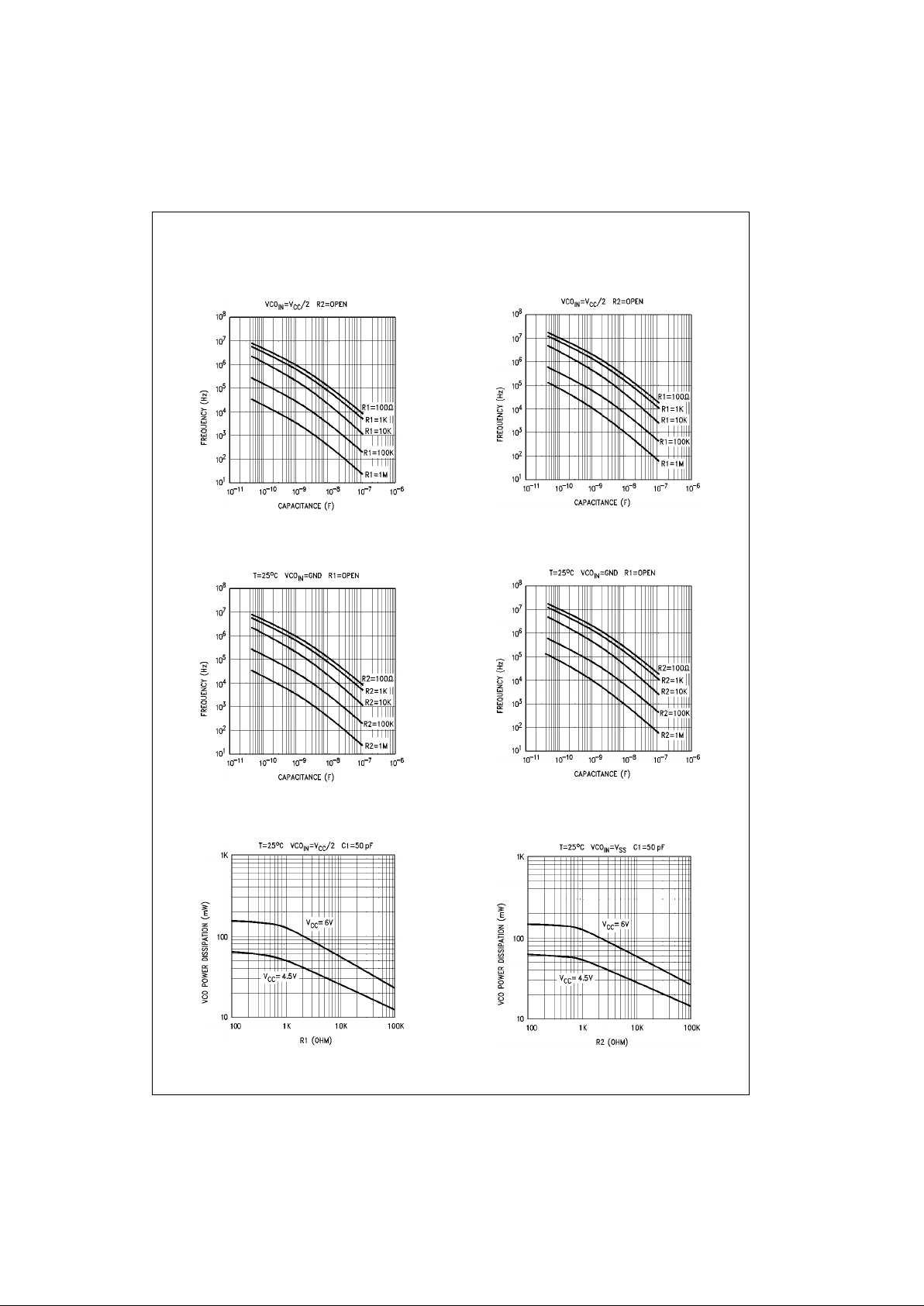
Typical Performance Characteristics
Typical Center Frequency
vs R1, C1 V
CC
= 4.5V
Typical Center Frequency
vs R1, C1 VCC = 6V
Typical Offset Frequency
vs R2, C1 V
CC
= 4.5V
Typical Offset Frequency
vs R2, C1 VCC = 6V
Typical VCO Power Dissipation
@ Center Frequency vs R1
Typical VCO Power
Dissipation @ f
min
vs R2
Page 6

www.fairchildsemi.com 6
MM74HC4046
Typical Performance Characteristics (Continued)
VCO
in
vs f
outVCC
= 4.5V VCOin vs f
outVCC
= 4.5V
VCO
out
vs
Temperature V
CC
= 4.5V
VCO
out
vs
Temperature V
CC
= 6V
Page 7
7 www.fairchildsemi.com
MM74HC4046
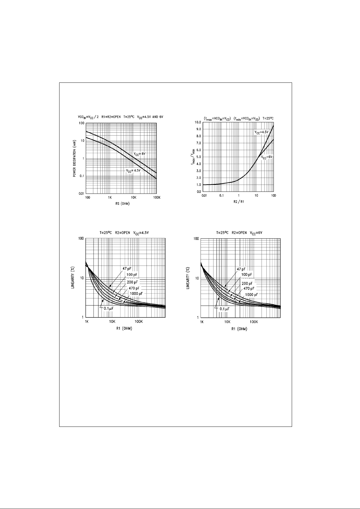
Typical Performance Characteristics (Continued)
HC4046 Typical Source Follower
Power Dissipation vs RS
Typical f
max/fmin
vs R2/R1
V
CC
= 4.5V & 6V f
max/fmin
Typical VCO Linaearity vs R1 & C1 Typical VCO Linearity vs R1 & C1
Page 8
www.fairchildsemi.com 8
MM74HC4046
Detailed Circuit Description
VOLTAGE CONTROLLED OSCILLATOR/SOURCE
FOLLOWER
The VCO requires two or three external components to
operate. These are R1, R2, C1. Resistor R1 and capacitor
C1 are selected to deter mine the center frequency of th e
VCO. R1 controls the lock range. As R1’s resistance
decreases the range of f
min
to f
max
increases. Thus the
VCO’s gain decreases. As C1 is changed the offset (if
used) of R2, and the center frequency is changed. (See
typical performance curve s) R2 can be used to set the offset frequency with 0V at VCO input. If R2 is omitted the
VCO range is from 0Hz. As R2 is decrea sed the offset frequency is increased. The effect of R2 is shown in the
design information table and typical performance curves.
By increasing the va lue of R2 th e lock rang e of the PLL is
offset above 0Hz and the gain (Volts/rad.) does not
change. In general, when offset is desired, R2 and C1
should be chosen f irst, and then R1 s hould be chosen to
obtain the proper center frequency.
Internally the resistors set a curre nt in a current mirror as
shown in Figure 1. T he m irrored curre nt dr ives o ne side of
the capacitor once the ca pacitor cha rges up to the threshold of the schmitt trigger the oscillator logic flips the capacitor over and ca uses th e mir ror t o cha rge t he op posi te side
of the capacitor. The output from the internal logic is then
taken to pin 4.
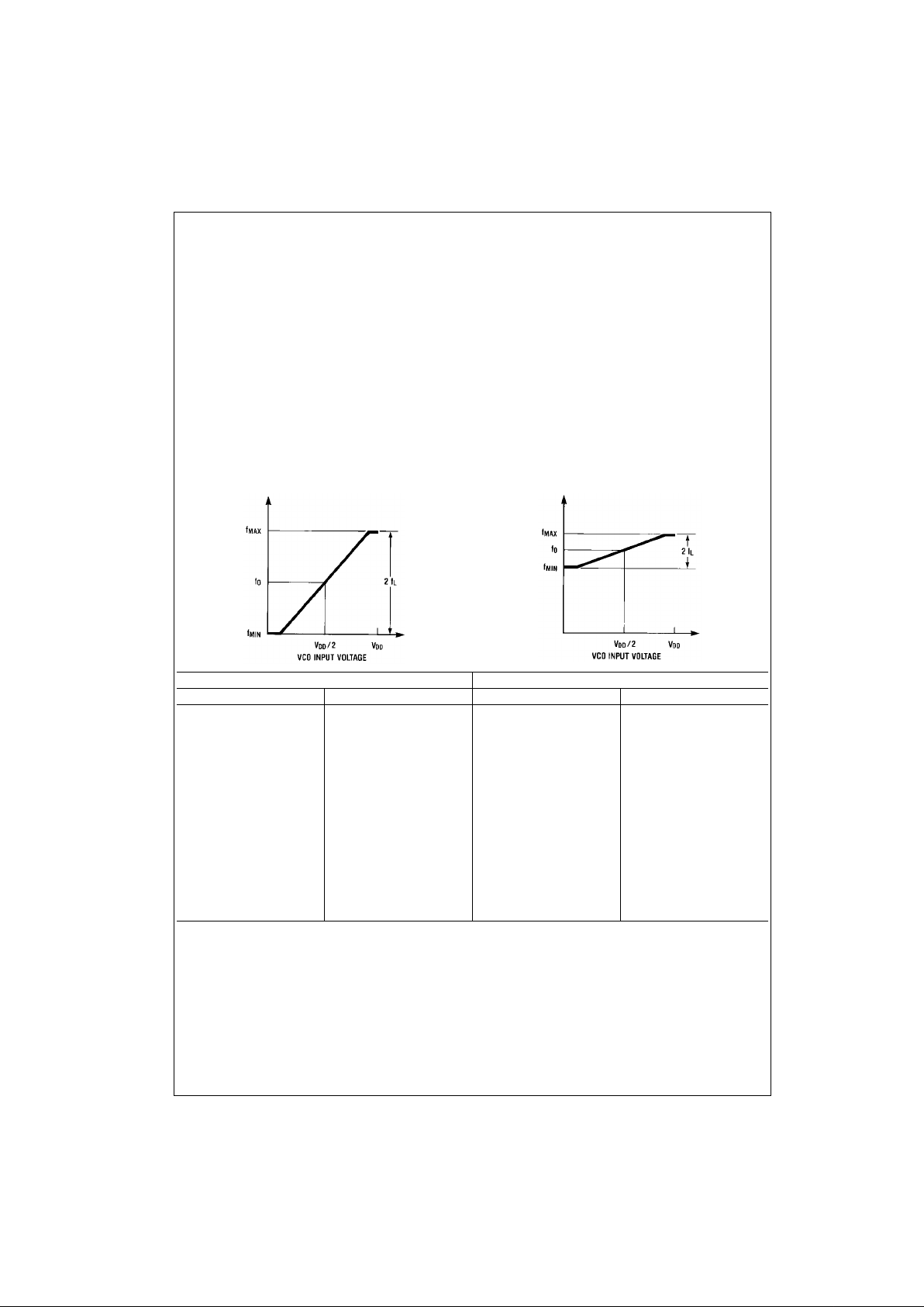
VCO WITHOUT OFFSET
R2 = ∞
VCO WITHOUT OFFSET
FIGURE 1.
Comparator I Comparator II & III
R
2
= ∞ R2≠∞ R2= ∞ R2≠∞
•Given: f
0
•Given: f0and f
L
•Given: f
max
•Given: f
min
and f
max
•Use f0 with curve titled •Calculate f
min
from the •Calculate f0 from the •Use f
min
with curve titled
center frequency vs R1, C equation f
min
= fo − f
L
equation fo = f
max
/2 offset frequency vs R2,
to determine R1 and C1 •Use f
min
with curve titled •Use f0 with curve titled C to determine R2 and C1
offset frequency vs R2, C center frequency vs R1, C •Calculate f
max/fmin
to determine R2 and C1 to determine R1 and C1 •Use f
max/fmin
with curve
•Calculate f
max/fmin
from titled f
max/fmin
vs R2/R1
the equation f
max/fmin
= to determine ratio R2/R1
f
o
+ fL/fo − f
L
to obtain R1
•Use f
max/fmin
with curve
titled f
max/fmin
vs R2/R1
to determine ratio R2/R1
to obtain R1
Page 9

9 www.fairchildsemi.com
MM74HC4046
FIGURE 2. Logic Diagram for VCO
The input to the VCO is a very high impedance CMOS
input and so it will not load down the loop filter, easing the
filters design. In order t o make signals at the VCO input
accessible without degrading the loop performance a
source follower transistor is provided. This transistor can
be used by connecting a resistor to groun d and its drain
output will follow the VCO input signal.
An inhibit signal is provide d to allow disabling of th e VCO
and the source follower. This is useful if the internal VCO is
not being used. A logic high on inhibit disa bles the VCO
and source follower.
The output of th e VCO is a standard high speed CMOS
output with an equivalent LSTTL fanout of 10. The VCO
output is approximately a square wave. This output can
either directly feed the com pa rat or in pu t of t he phase comparators or feed ex ternal prescalers (counters) to enable
frequency synthesis.
PHASE COMPARATORS
All three phase comparators share two inputs, Signal In
and Comparator In. The Signal In has a special DC bias
network that enables AC coupling of input signals. If the
signals are not AC couple d then this input requires logic
levels the same as standard 74HC. The Comparator i nput
is a standard digital input. Both i nput structur es are shown
in Figure 3.
The outputs of the se com parato rs are essent ially sta ndard
74HC voltage outputs. (Comparator II is 3-STATE.)
FIGURE 3. Logic Diagram for Phase Comparator I and the common input circuit for all three comparators
Page 10
www.fairchildsemi.com 10
MM74HC4046
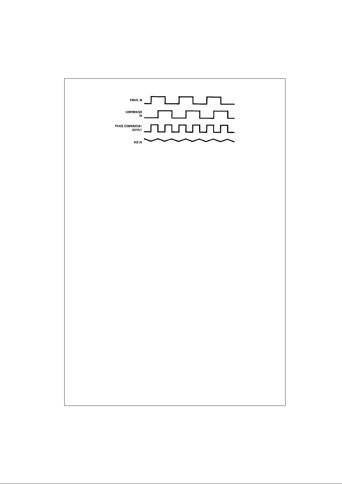
FIGURE 4. Typical Phase Comparator I. Waveforms
Thus in normal oper ation V
CC
and ground voltage le vels
are fed to the loop filter. This differs from some phase
detectors which supply a current output to the loop filter
and this should be considered in the design. (The CD4046
also provides a voltage.)
Figure 5 shows the state tables for all three comparators.
PHASE COMPARATOR I
This comparator is a simple XOR gate similar to the
74HC86, and its oper ation is similar to an over driven balanced modulator. To maximize lock range the input frequencies must have a 50% duty cycle. Typical input and
output waveforms are shown in Figure 4. The out put of th e
phase detector feeds the loop filter which averages the output voltage. The frequency range upon which the PLL will
lock onto if initially out of lock is defined as the capture
range. The capture range for phase detector I is dependent
on the loop filter employe d. The capture range ca n be as
large as the lock range which is equal to the VCO frequency range.
To see how the detector operates refer to Figure 4. Whe n
two square wave inp uts are ap plied to this compar ator, an
output waveform whose duty cycle is dependent on the
phase difference betwe en the two signals results . As the
phase difference increases th e o utpu t du ty cycle increases
and the voltage after the loop filter increases. Thus in order
to achieve lock, when th e PLL input frequency increases
the VCO input volta ge mu st incre ase and th e phas e difference between comparator in and signal in will increase. At
an input frequency equal f
min
, the VCO input is at 0V and
this requires the phase de tect or ou tpu t to be ground hence
the two input signals must be in phase. When the input fre-
quency is f
max
then the VCO input must be VCC and the
phase detector inputs must be 180° out of phase.
The XOR is more sus cepti ble to lo cking onto h armon ics of
the signal input than the d igital phas e detector II . This can
be seen by noticing that a signal 2 times the VCO frequency results in the same outpu t duty cycle as a signal
equal the VCO freque ncy. The difference is t hat the output
frequency of the 2f example is twice that of the other example. The loop filter and the VCO ra nge shou ld be design ed
to prevent locking on to harmonics.
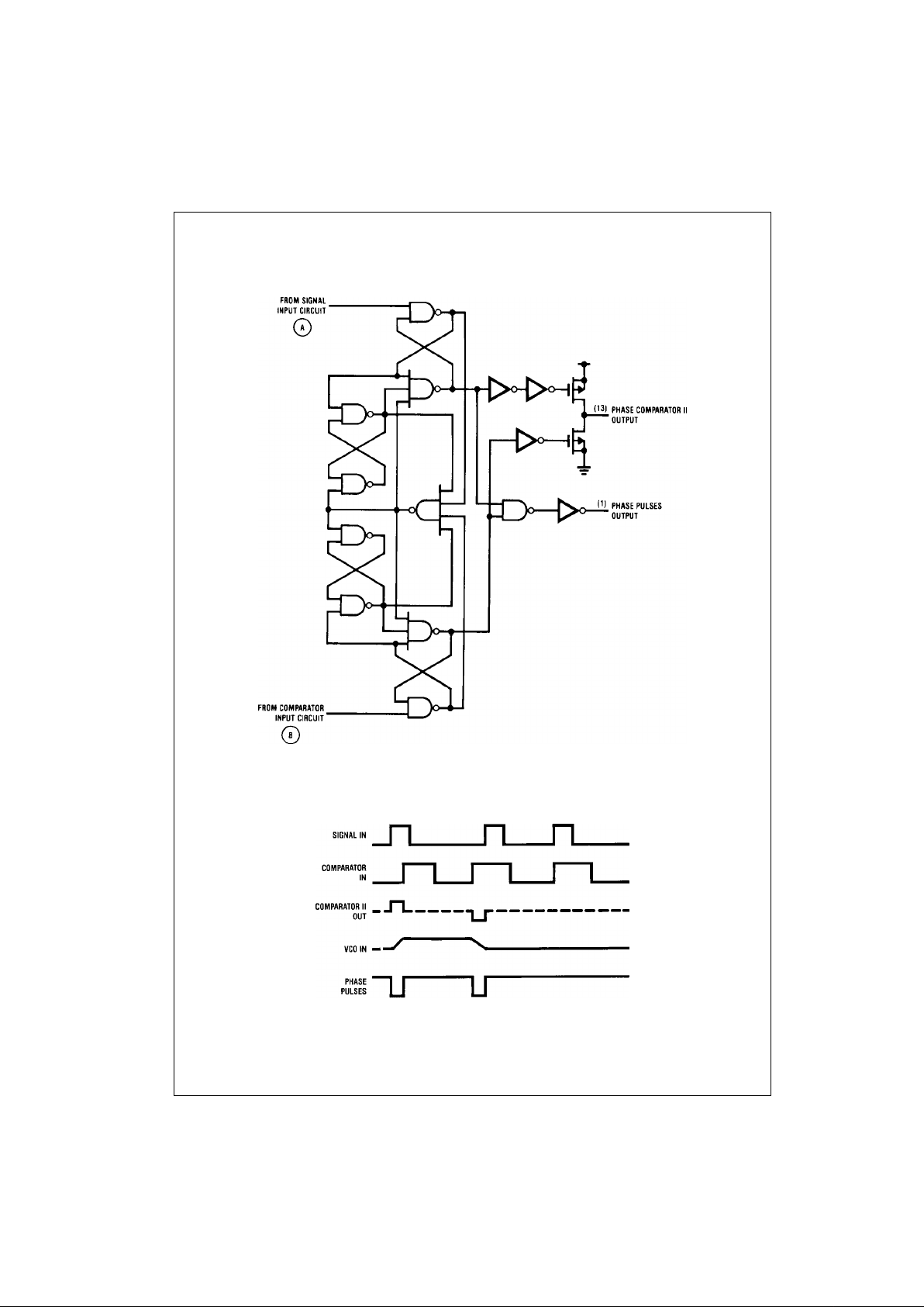
PHASE COMPARATOR II
This detector is a digital memory network. It consists of four
flip-flops and some gating logic, a three state outp ut an d a
phase pulse output a s sho wn in Fi gur e 6. Th is co mpara tor
acts only on the po sitive edges of the inpu t signals an d is
thus independent of signal duty cycle.
Phase comparator II operates in such a way as to force the
PLL into lock with 0 phase difference betw een the VCO
output and the signal input posit ive waveform edges. Figure 7 shows some typical loop waveforms. First assume
that the signal input phase is leading the c om par ato r inp ut.
This means that the VCO’s frequency must be increased to
bring its leading edg e into proper phase alignm ent. Thus
the phase detector II output is set high. This will ca use the
loop filter to charge up th e VCO input increa sing the VCO
frequency. Once the leading edge of t he comparato r input
is detected the output goes 3-STATE holding the VCO
input at the loop filter voltage. If th e VCO still lags the signal then the phase detector will again charge up to VCO
input for the time between the leading edges of both waveforms.
Page 11

11 www.fairchildsemi.com
MM74HC4046
Phase Comparator State Dia gra ms
FIGURE 5. PLL State Tables
Page 12
www.fairchildsemi.com 12
MM74HC4046
FIGURE 6. Logic Diagram for Phase Comparator II
FIGURE 7. Typical Phase Comparator II Output Waveforms
Page 13

13 www.fairchildsemi.com
MM74HC4046
If the VCO leads the signal then when the leading edge of
the VCO is seen the output of the phase comparator go es
LOW. This discharges the loop filte r until the leading edge
of the signal is detected at wh ich time the out put 3-STATE
itself again. This has the effect of slowing down the VCO to
again make the rising edges of both waveform coincident.
When the PLL is out of lock the VCO will be running either
slower or faster than the sign al inpu t. If it is ru nning slow er
the phase detector will see more signal rising edges and so
the output of the phase comparator will be HIGH a majority
of the time, raising the VCO ’s frequency. Conversely, if the
VCO is running faster than the signal the output of the
detector will be LOW most of the time and the VCO’s output frequency will be decreased.
As one can see when the PLL is locked the output of phase
comparator II will be almos t always 3-STATE except for
minor corrections at the leading edge of the waveforms.
When the detector is 3- STATE the phase pulse output is
HIGH. This output can be used to determine when the PLL
is in the locked condition.
This detector has several inter esting characteristics. Over
the entire VCO frequency range there is no phase difference between the c omparator input and the si gnal input.
The lock range of the PLL is the same as the capture
range. Minimal power is consumed in the loop filter since in
lock the detector output is a high impedance. Also when no
signal is present the detector will see only VCO leading
edges, and so the comparator output will stay LOW forcing
the VCO to f
min
operating frequency.
Phase comparator II is more suscepti ble to noise causing
the phase lock loop to unlock. If a noise pulse is seen on
the signal input, the comparator treats it as another positive
edge of the signal and will cause the output to go HIGH
until the VCO leading edge is seen, potentially fo r a whole
signal input period. This would cause the VCO to speed up
during that time. W hen using the phase com parator I the
output of that phase detector would be disturb ed for only
the short duration of the noise sp ike and wou ld c ause les s
upset.
PHASE COMPARATOR III
This comparator is a simple S-R Flip-Flop which can function as a phase comparator Figure 8. It has some similar
characteristics to the edge se nsitive comparator. To see
how this detector works assume input pulses are applied to
the signal and comparator inputs as shown in Figure 9.
When the signal input leads the comparator input the flop is
set. This will charge up the loop filter and cause the VCO to
speed up, bringing th e comp arato r into p hase wi th the signal input. When using short pulses as input this comparator
behaves very similar to t he second comparator. But one
can see that if the signal input is a long pulse, the output of
the comparator will be forced to a one no matter how many
comparator input pulses are received. Also if the VCO input
is a square wave (as it is) and the signal input is pulse then
the VCO will force the comparator output LOW much of the
time. Therefore it is ideal to condi tion the signa l and comparator input to short pulses. This is most easily done by
using a series capacitor.
FIGURE 8. Phase Comparator III Logic Diagram
FIGURE 9. Typical Waveforms for Phase Comparator III
Page 14

www.fairchildsemi.com 14
MM74HC4046
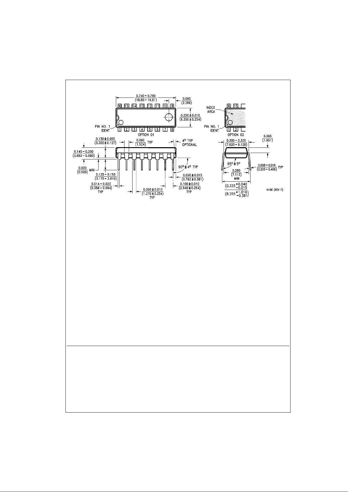
Physical Dimensions inches (millimeters) unless otherwise noted
16-Lead Small Outline Integrated Circuit (SOIC), JEDEC MS-012, 0.150” Narrow
Package Number M16A
16-Lead Small Outline Package (SOP), EIAJ TYPE II, 5.3mm Wide
Package Number M16D
Page 15

15 www.fairchildsemi.com
MM74HC4046
Physical Dimensions inches (millimeters) unless otherwise noted (Continued)
16-Lead Thin Shrink Small Outline Package (TSSOP), JEDEC MO-153, 4.4mm Wide
Package Number MTC16
Page 16
Fairchild does not assume any responsibility for use of any circuitry described, no circuit patent licenses are implied and Fairchild reserves the right at any time without notice to change said circuitry and specifications.
MM74HC4046 CMOS Phase Lock Loop
LIFE SUPPORT POLICY
FAIRCHILD’S PRODUCTS ARE NOT AUTHORIZED FOR USE AS CRITICAL COMPONENTS IN LIFE SUPPORT
DEVICES OR SYSTEMS WITHOUT THE EXPRESS WRITTEN APPROVAL OF THE PRESIDENT OF FAIRCHILD
SEMICONDUCTOR CORPORATION. As used herein:
1. Life support devices or systems are devices or syste ms
which, (a) are intended for surgical implant into the
body, or (b) support or sustain life, and (c) whose failure
to perform when properly used in accordance with
instructions for use provided in the labeling, can be reasonably expected to result in a significant inju ry to the
user.
2. A critical component i n any compon ent of a lif e support
device or system whose failu re to perform can be reasonably expected to ca use the fa i lure of the life su pp ort
device or system, or to affect its safety or effectiveness.
www.fairchildsemi.com
Physical Dimensions inches (millimeters) unless otherwise noted (Continued)
16-Lead Plastic Dual-In-Line Package (PDIP), JEDEC MS-001, 0.300” Wide
Package Number N16E
 Loading...