

Datasheet MM74HC4040SJX, MM74HC4040N, MM74HC4040CW, MM74HC4040SJ, MM74HC4040M Datasheet (Fairchild Semiconductor)
...Page 1
February 1984
Revised February 1999
MM74HC4020 • MM74HC4040 14-Stage Binary Counter • 12-Stage Binary Counter
© 1999 Fairchild Semiconductor Corporation DS005216.prf www.fairchildsemi.com
MM74HC4020 • MM74HC4040
14-Stage Binary Counter • 12-Stage Binary Counter
General Description
The MM74HC4020, M M74HC4040 , are high spe ed binary
ripple carry counters . These counters are i mple me nte d u tilizing advanced silicon- gate CMOS technology to ach ieve
speed performance similar to LS-TTL logic while retaining
the low power and high noise immunity of CMOS.
The MM74HC4020 is a 14 stage counter and the
MM74HC4040 is a 12-stage counter. Both devices are
incremented on the falling edge (negative transition) of t he
input clock, and all th eir outp uts ar e reset to a l ow leve l by
applying a logical high on their reset input.
These devices are pin equivalent to the CD4020 and
CD4040 respectively. All inputs are protected from damage
due to static discharge by pr otection diodes to V
CC
and
ground.
Features
■ Typical propagation delay: 16 ns
■ Wide operating voltage range: 2–6V
■ Low input current: 1 µA maximum
■ Low quiescent current: 80 µA maximum (74HC Series)
■ Output drive capability: 10 LS-TTL loads
Ordering Code:
Devices also availab le in Tape and Reel. Specify by appending th e s uffix let t er “X” to the ordering cod e.
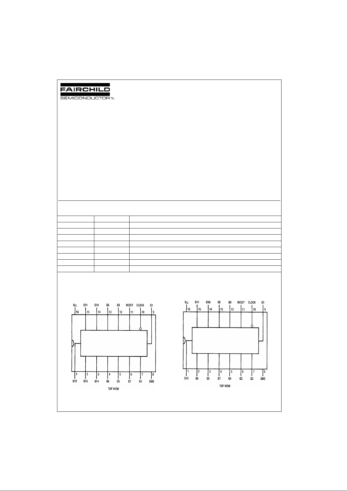
Connection Diagrams
Pin Assignments for DIP, SOIC, SOP and TSSOP
MM74HC4020
MM74HC4040
Order Number Package Number Package Description
MM74HC4020M M16A 16-Lead Small Outline Integrated Circuit (SOIC), JEDEC MS-012, 0.150” Narrow
MM74HC4020SJ M16D 16-Lead Small Outline Package (SOP), EIAJ TYPE II, 5.3mm Wide
MM74HC4020MTC MTC16 16-Lead Thin Shrink Small Outline Package (TSSOP), JEDEC MO-153, 4.4mm Wide
MM74HC4020N N16E 16-Lead Plastic Dual-In-Line Package (PDIP), JEDEC MS-001, 0.300” Wide
MM74HC4040M M16A 16-Lead Small Outline Integrated Circuit (SOIC), JEDEC MS-012, 0.150” Narrow
MM74HC4040SJ M16D 16-Lead Small Outline Package (SOP), EIAJ TYPE II, 5.3mm Wide
MM74HC4040MTC MTC16 16-Lead Thin Shrink Small Outline Package (TSSOP), JEDEC MO-153, 4.4mm Wide
MM74HC4040N N16E 16-Lead Plastic Dual-In-Line Package (PDIP), JEDEC MS-001, 0.300” Wide
Page 2
www.fairchildsemi.com 2
MM74HC4020 • MM74HC4040
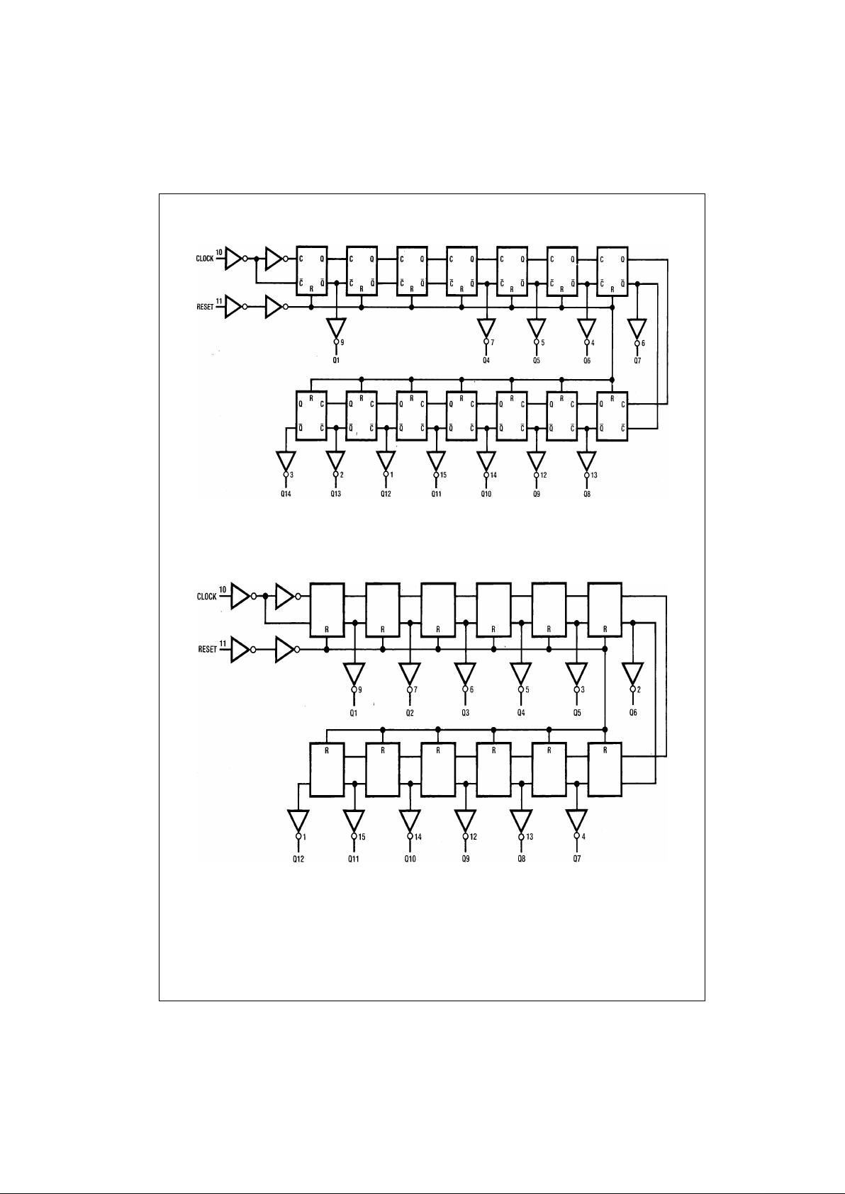
Logic Diagrams
MM74HC4020
MM74HC4040
Page 3
3 www.fairchildsemi.com
MM74HC4020 • MM74HC4040
Absolute Maximum Ratings(Note 1)
(Note 2)
Recommended Operating
Conditions
Note 1: Maximum Ratings are those values beyond which damage to the
device may occur.
Note 2: Unless otherwise specified all voltages are referenced to ground.
Note 3: Power Dissipation te mperature d erating — pl astic “N” pa ckage: −
12 mW/°C from 65°C to 85°C.
DC Electrical Characteristics (Note 4)
Note 4: For a powe r supply o f 5V ±10% the worst case output voltages (VOH, and VOL) occur for HC at 4.5V. Thus the 4. 5V valu es shou ld be u sed when
designing with this supply. Worst case V
IH
and VIL occur at V
CC
= 5.5V and 4.5V respectively. (The VIH value at 5.5V is 3 .8 5V.) The worst c as e leakage cur-
rent (I
IN
, ICC, and IOZ) occur for CMOS at the higher voltage and so th e 6. 0V values should be used.
Supply Voltage (VCC) −0.5 to +7.0V
DC Input Voltage (V
IN
) −1.5 to V
CC
+1.5V
DC Output Voltage (V
OUT
) −0.5 to V
CC
+0.5V
Clamp Diode Current (I
CD
) ±20 mA
DC Output Current, per pin (I
OUT
) ±25 mA
DC V
CC
or GND Current, per pin (ICC) ±50 mA
Storage Temperature Range (T
STG
) −65°C to +150°C
Power Dissipation (P
D
)
(Note 3) 600 mW
S.O. Package only 500 mW
Lead Temperature (T
L
)
(Soldering 10 seconds) 260°C
Min Max Units
Supply Voltage (V
CC
)26V
DC Input or Output Voltage 0 V
CC
V
(V
IN
, V
OUT
)
Operating Temperature Range (T
A
) −40 +85 °C
Input Rise or Fall Times
(t
r
, tf) V
CC
= 2.0V 1000 ns
V
CC
= 4.5V 500 ns
V
CC
= 6.0V 400 ns
Symbol Parameter Conditions
V
CC
TA = 25°CTA = −40 to 85°CTA = −55 to 125°C
Units
Typ Guaranteed Limits
V
IH
Minimum HIGH Level Input 2.0V 1.5 1.5 1.5 V
Voltage 4.5V 3.15 3.15 3.15 V
6.0V 4.2 4.2 4.2 V
V
IL
Maximum LOW Level Input 2.0V 0.5 0.5 0.5 V
Voltage 4.5V 1.35 1.35 1.35 V
6.0V 1.8 1.8 1.8 V
V
OH
Minimum HIGH Level Output V
IN
= VIH or V
IL
Voltage |I
OUT
| ≤ 20 µA 2.0V 2.0 1.9 1.9 1.9 V
4.5V 4.5 4.4 4.4 4.4 V
6.0V 6.0 5.9 5.9 5.9 V
V
IN
= VIH or V
IL
|I
OUT
| ≤ 4.0 mA 4.5V 4.2 3.98 3.84 3.7 V
|I
OUT
| ≤ 5.2 mA 6.0V 5.7 5.48 5.34 5.2 V
V
OL
Maximum LOW Level Output V
IN
= VIH or V
IL
Voltage |I
OUT
| ≤ 20 µA 2.0V 0 0.1 0.1 0.1 V
4.5V 0 0.1 0.1 0.1 V
6.0V 0 0.1 0.1 0.1 V
V
IN
= VIH or V
IL
|I
OUT
| ≤ 4.0 mA 4.5V 0.2 .26 0.33 0.4 V
|I
OUT
| ≤ 5.2 mA 6.0V 0.2 .26 0.33 0.4 V
I
IN
Maximum Input Current V
IN
= VCC or GND 6.0V ±0.1 ±1.0 ±1.0 µA
I
CC
Maximum Quiescent Supply V
IN
= VCC or GND 6.0V 8.0 80 160 µA
Current I
OUT
= 0 µA
Page 4

www.fairchildsemi.com 4
MM74HC4020 • MM74HC4040
AC Electrical Characteristics
V
CC
= 5V, TA = 25°C, CL = 15 pF, tr = t
f
= 6 ns
Note 5: Typical Propagatio n delay time to any output c an be calculated using: tP= 17 + 12(N–1) ns; where N is the number of the output, QW, at V
CC
= 5V.
AC Electrical Characteristics
V
CC
= 2.0V to 6.0V, CL = 50 pF, tr = t
f
= 6 ns (unless otherwise specified)
Note 6: CPD determines the no lo ad dynamic power con s um ption, PD = CPD V
CC
2
f + ICC VCC, and the no load dynam ic cu rrent consumption,
I
S
= CPDVCCf + ICC.
Symbol Parameter Conditions Typ
Guaranteed
Units
Limit
f
MAX
Maximum Operating Frequency 50 30 MHz
t
PHL
, t
PLH
Maximum Propagation (Note 5) 17 35 ns
Delay Clock to Q
t
PHL
Maximum Propagation 16 40 ns
Delay Reset to any Q
t
REM
Minimum Reset 10 20 ns
Removal Time
t
W
Minimum Pulse Width 10 16 ns
Symbol Parameter Conditions
V
CC
TA = 25°CTA = −40 to 85°CTA = −55 to 125°C
Units
Typ Guaranteed Limits
f
MAX
Maximum Operating 2.0V 10 6 5 4 MHz
Frequency 4.5V 40 30 24 20 MHz
6.0V 50 35 28 24 MHz
t
PHL
, t
PLH
Maximum Propagation 2.0V 80 210 265 313 ns
Delay Clock to Q
1
4.5V 21 42 53 63 ns
6.0V 18 36 45 53 ns
T
PHL, tPLH
Maximum Propagation 2.0V 80 125 156 188 ns
Delay Between Stages 4.5V 18 25 31 38 ns
from Qn to Q
n+1
6.0V 15 21 26 31 ns
t
PHL
Maximum Propagation 2.0V 72 240 302 358 ns
Delay Reset to any Q 4.5V 24 48 60 72 ns
(4020 and 4040) 6.0V 20 41 51 61 ns
t
REM
Minimum Reset 2.0V 100 126 149 ns
Removal Time 4.5V 20 25 50 ns
6.0V 16 21 25 ns
t
W
Minimum Pulse Width 2.0V 90 100 120 ns
4.5V 16 20 24 ns
6.0V 14 18 20 ns
t
TLH
, t
THL
Maximum 2.0V 30 75 95 110 ns
Output Rise 4.5V 10 15 19 22 ns
and Fall Time 6.0V 9 13 16 19 ns
tr, t
f
Maximum Input Rise and 1000 1000 1000 ns
Fall Time 500 500 500 ns
400 400 400 ns
C
PD
Power Dissipation (per package) 55 pF
Capacitance (Note 6)
C
IN
Maximum Input 5 10 10 10 pF
Capacitance
Page 5

5 www.fairchildsemi.com
MM74HC4020 • MM74HC4040
Timing Diagram
Page 6

www.fairchildsemi.com 6
MM74HC4020 • MM74HC4040
Physical Dimensions inches (millimeters) unless otherwise noted
16-Lead Small Outline Integrated Circuit (SOIC), JEDEC MS-012, 0.150” Narrow
Package Number M16A
16-Lead Small Outline Package (SOP), EIAJ TYPE II, 5.3mm Wide
Package Number M16D
Page 7

7 www.fairchildsemi.com
MM74HC4020 • MM74HC4040
Physical Dimensions inches (millimeters) unless otherwise noted (Continued)
16-Lead Thin Shrink Small Outline Package (TSSOP), JEDEC MO-153, 4.4mm Wide
Package Number MTC16
Page 8

Fairchild does not assume any responsibility for use of any circuitry described, no circuit patent licenses are implied and Fairchild reserves the right at any time without notice to change said circuitry and specifications.
MM74HC4020 • MM74HC4040 14-Stage Binary Counter • 12-Stage Binary Counter
LIFE SUPPORT POLICY
FAIRCHILD’S PRODUCTS ARE NOT AUTHORIZED FOR USE AS CRITICAL COMPONENTS IN LIFE SUPPORT
DEVICES OR SYSTEMS WITHOUT THE EXPRESS WRITTEN APPROVAL OF THE PRESIDENT OF FAIRCHILD
SEMICONDUCTOR CORPORATION. As used herein:
1. Life support devices or systems are devices or syste ms
which, (a) are intended for surgical implant into the
body, or (b) support or sustain life, and (c) whose failure
to perform when properly used in accordance with
instructions for use provided in the labeling, can be reasonably expected to result in a significant inju ry to the
user.
2. A critical component i n any compon ent of a lif e support
device or system whose failu re to perform can be reasonably expected to ca use the fa i lure of the life su pp ort
device or system, or to affect its safety or effectiveness.
www.fairchildsemi.com
Physical Dimensions inches (millimeters) unless otherwise noted (Continued)
16-Lead Plastic Dual-In-Line Package (PDIP), JEDEC MS-001, 0.300” Wide
Package Number N16E
 Loading...