

Datasheet MM74HC374WMX, MM74HC374SJX, MM74HC374N, MM74HC374MTC, MM74HC374WM Datasheet (Fairchild Semiconductor)
...Page 1
September 1983
Revised February 1999
MM74HC374 3-STATE Octal D-Type Flip-Flop
© 1999 Fairchild Semiconductor Corporation DS005336.prf www.fairchildsemi.com
MM74HC374
3-STATE Octal D-Type Flip-Flop
General Description
The MM74HC374 hi gh speed Octal D -Type Flip-Flops utilize advanced silicon-gate CMOS technology. They possess the high noise im munity and low power consumption
of standard CMOS integrated circuits, as well as the ability
to drive 15 LS-TTL loads. Due to the large output drive
capability and the 3-STATE feature, these devices are ideally suited for interfacing with bus lines in a bus organized
system.
These devices are positive edge triggered flip- flops. Data
at the D inputs, meeting the setup and hold tim e requirements, are transferred to the Q outputs on positive going
transitions of the CLOCK (CK) input. When a high logic
level is applied to the OUTPUT CONTROL (OC) input, all
outputs go to a high impedance state, regard less of what
signals are present at the oth er inputs and the state of the
storage elements.
The 74HC logic family is speed, function, and pinou t compatible with the standard 74 LS logic family. All inputs are
protected from damage due to static discharge by internal
diode clamps to V
CC
and ground.
Features
■ Typical propagation delay: 20 ns
■ Wide operating voltage range: 2–6V
■ Low input current: 1 µA maximum
■ Low quiescent current: 80 µA maximum
■ Compatible with bus-oriented systems
■ Output drive capability: 15 LS-TTL loads
Ordering Code:
Devices also available in Tape and Reel. Specify by appending the suffix letter “X” to t he ordering code.
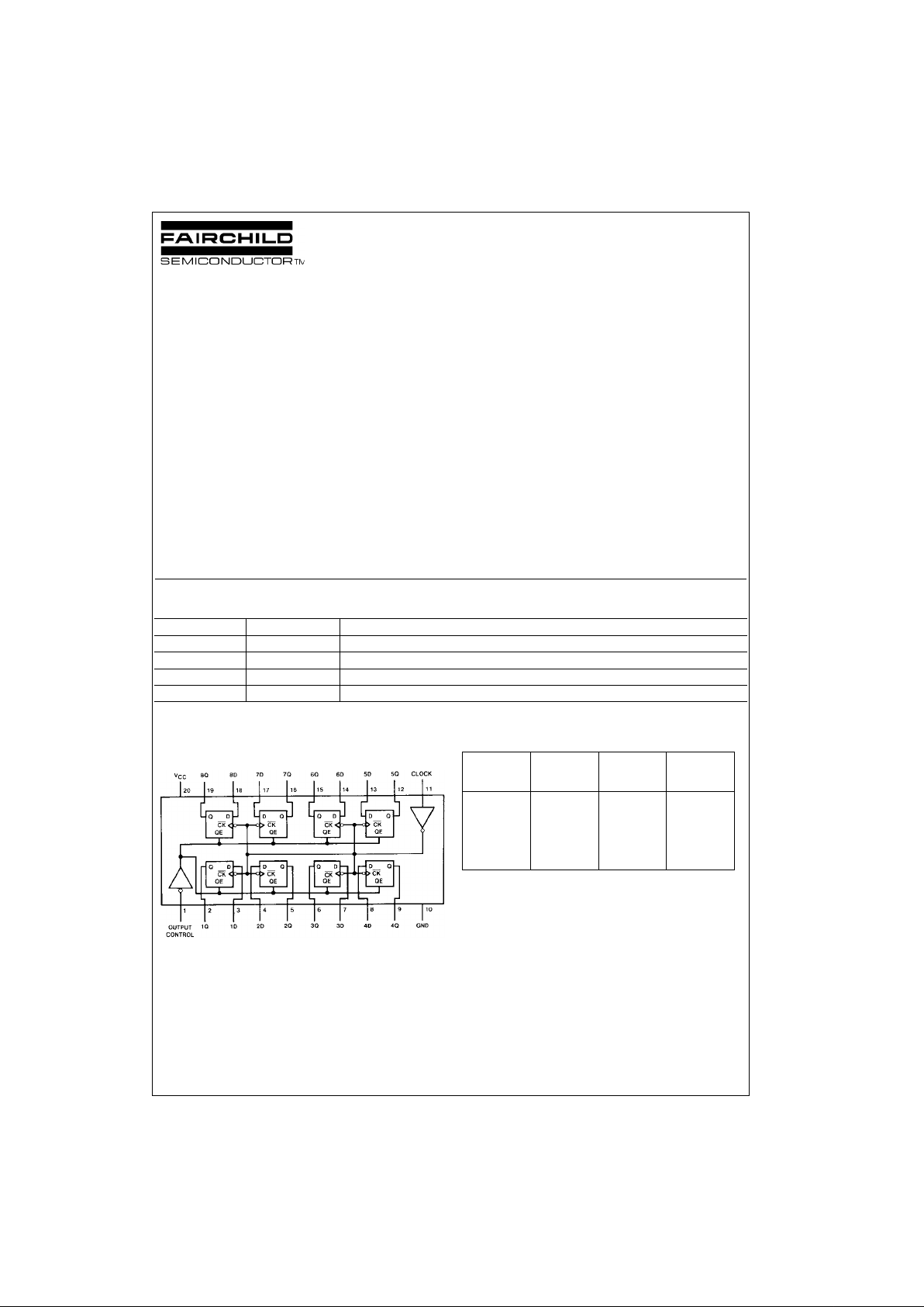
Connection Diagram
Pin Assignments for DIP, SOIC, SOP and TSSOP
Top View
Truth Table
H = HIGH Level
L = LOW Level
X = Don't Care
↑ = Transition from LOW-to-HIGH
Z = High Impedance Stat e
Q
0
= The l evel of the out put before steady state input conditions were
established
Order Number Package Number Package Description
MM74HC374WM M20B 20-Lead Small Outline Integrated Circuit (SOIC), JEDEC MS-013, 0.300” Wide
MM74HC374SJ M20D 20-Lead Small Outline Package (SOP), EIAJ TYPE II, 5.3mm Wide
MM74HC374MTC MTC20 20-Lead Thin Shrink Small Outline Package (TSSOP), JEDEC MO-153, 4.4mm Wide
MM74HC374N N20A 20-Lead Plastic Dual-In-Line Package (PDIP), JEDEC MS-001, 0.300” Wide
Output Clock Data Output
Control
L ↑ HH
L ↑ LL
LLXQ
0
HXXZ
Page 2
www.fairchildsemi.com 2
MM74HC374
Absolute Maximum Ratings(Note 1)
(Note 2)
Recommended Operating
Conditions
Note 1: Absolute Maximum Ratings are those values beyond which dam-
age to the device may occur.
Note 2: Unless otherwise specified all voltages are referenced to ground.
Note 3: Power Dissipation temperat ure derat ing — plas tic “N” p ackage: −
12 mW/°C from 65 °C to 85°C.
DC Electrical Characteristics
Note 4: For a power supply of 5V ±10% the wors t case outpu t voltages (VOH, and VOL) occur for HC at 4.5 V. Thus the 4.5V values s hould b e used when
designing with this supply. Worst case V
IH
and VIL occur at V
CC
= 5.5V and 4.5V respectively. (The VIH value at 5.5V is 3.85V.) The worst case leakage cur-
rent (I
IN
, ICC, and IOZ) occur for CMOS at the higher voltage and so the 6.0V values s hould be used.
Supply Voltage (VCC) −0.5 to +7.0V
DC Input Voltage (V
IN
) −1.5 to V
CC
+1.5V
DC Output Voltage (V
OUT
) −0.5 to V
CC
+0.5V
Clamp Diode Current (I
IK
, IOK) ±20 mA
DC Output Current, per pin (I
OUT
) ±35 mA
DC V
CC
or GND Current, per pin (ICC) ±70 mA
Storage Temperature Range (T
STG
) −65°C to +150°C
Power Dissipation (P
D
)
(Note 3) 600 mW
S.O. Package only 500 mW
Lead Temperature (T
L
)
(Soldering 10 seconds) 260°C
Min Max Units
Supply Voltage (V
CC
)26V
DC Input or Output Voltage
(V
IN
, V
OUT
)0V
CC
V
Operating Tempera ture Range (T
A
) −40 +85 °C
Input Rise or Fall Times
(t
r
, tf) V
CC
= 2.0V 1000 ns
V
CC
= 4.5V 500 ns
V
CC
= 6.0V 400 ns
Symbol Parameter Conditions
V
CC
TA = 25°CTA = −40 to 85°CTA = −55 to 125°C
Units
Typ Guaranteed Limits
V
IH
Minimum HIGH Level 2.0V 1.5 1.5 1.5 V
Input Voltage 4.5V 3.15 3.15 3.15 V
6.0V 4.2 4.2 4.2 V
V
IL
Maximum LOW Level 2.0V 0.5 0.5 0.5 V
Input Voltage 4.5V 1.35 1.35 1.35 V
6.0V 1.8 1.8 1.8 V
V
OH
Minimum HIGH Level V
IN
= VIH or V
IL
Output Voltage |I
OUT
| ≤ 20 µA 2.0V 2.0 1.9 1.9 1.9 V
4.5V 4.5 4.4 4.4 4.4 V
6.0V 6.0 5.9 5.9 5.9 V
V
IN
= VIH or V
IL
|I
OUT
| ≤ 6.0 mA 4.5V 4.2 3.98 3.84 3.7 V
|I
OUT
| ≤ 7.8 mA 6.0V 5.7 5.48 5.34 5.2 V
V
OL
Maximum LOW Level V
IN
= VIH or V
IL
Output Voltage |I
OUT
| ≤ 20 µA 2.0V 0 0.1 0.1 0.1 V
4.5V 0 0.1 0.1 0.1 V
6.0V 0 0.1 0.1 0.1 V
V
IN
= VIH or V
IL
|I
OUT
| ≤ 6.0 mA 4.5V 0.2 0.26 0.33 0.4 V
|I
OUT
| ≤ 7.8 mA 6.0V 0.2 0.26 0.33 0.4 V
I
IN
Maximum Input V
IN
= VCC or GND 6.0V ±0.1 ±1.0 ±1.0 µA
Current
I
OZ
Maximum 3- STATE V
IN
= VIH, OC = V
IH
6.0V ±0.5 ±5 ±10 µA
Output Leakage V
OUT
= VCC or GND
Current
I
CC
Maximum Quiescent V
IN
= VCC or GND 6.0V 8.0 80 160 µA
Supply Current I
OUT
= 0 µA
Page 3
3 www.fairchildsemi.com
MM74HC374
AC Electrical Characteristics
V
CC
= 5V, T
A
= 25°C, t
r
= t
f
= 6 ns
Symbol Parameter Conditions Typ
Guaranteed
Units
Limit
f
MAX
Maximum Operating 50 35 MHz
Frequency
t
PHL
, t
PLH
Maximum Propagation CL=45 pF 20 32 ns
Delay Clock to Q
t
PZH
, t
PZL
Maximum Output Enable RL= kΩ
Time CL=45 pF 19 28 ns
t
PHZ
, t
PLZ
Maximum Output Disable RL= kΩ 17 25 ns
Time CL=5 pF
t
S
Minimum Setup Time 20 ns
t
H
Minimum Hold Time 5ns
t
W
Minimum Pulse Width 9 16 ns
Page 4

www.fairchildsemi.com 4
MM74HC374
AC Electrical Charac teristics
V
CC
= 2.0−6.0V, CL = 50 pF, tr = t
f
= 6 ns (unless otherwise specified)
Note 5: CPD determines the no load dynamic power con s um ption, PD = CPD V
CC
2
f + ICC VCC, and the no load dynamic current consum pt ion,
I
S
= CPDVCCf + ICC.
Symbol Parameter Conditions
V
CC
TA = 25°CTA = −40 to 85°CTA = −55 to 125°C
Units
Typ Guaranteed Limits
f
MAX
Maximum Operating CL = 50 pF 2.0V 6 5 4 MHz
Frequency 4.5V 30 24 20 MHz
6.0V 35 28 23 MHz
t
PHL
, t
PLH
Maximum Propagation CL = 50 pF 2.0V 68 180 225 270 ns
Delay, Clock to Q CL = 150 pF 2.0V 110 230 288 345 ns
CL = 50 pF 4.5V 22 36 45 48 ns
CL = 150 pF 4.5V 30 46 57 69 ns
CL = 50 pF 6.0V 20 31 39 46 ns
CL = 150 pF 6.0V 28 40 50 60 ns
t
PZH
, t
PZL
Maximum Output RL = 1 kΩ
Enable Time CL = 50 pF 2.0V 50 150 189 225 ns
CL = 150 pF 2.0V 80 200 250 300 ns
CL = 50 pF 4.5V 21 30 37 45 ns
CL = 150 pF 4.5V 30 40 50 60 ns
CL = 50 pF 6.0V 19 26 31 39 ns
CL = 150 pF 6.0V 26 35 44 53 ns
t
PHZ
, t
PLZ
Maximum Output RL = 1 kΩ 2.0V 50 150 189 225 ns
Disable Time CL = 50 pF 4.5V 21 30 37 45 ns
6.0V 19 26 31 39 ns
t
S
Minimum Setup Time 2.0V 50 60 75 ns
4.5V 9 13 15 ns
6.0V 9 11 13 ns
t
H
Minimum Hold Time 2.0V 5 30 5 ns
4.5V 5 5 5 ns
6.0V 5 5 5 ns
t
W
Minimum Pulse Width 2.0V 30 80 100 120 ns
4.5V 9 16 20 24 ns
6.0V 8 14 18 20 ns
t
THL
, t
TLH
Maximum Output Rise CL = 50 pF 2.0V 25 60 75 90 ns
and Fall Time 4.5V 7 12 15 18 ns
6.0V 6 10 13 15 ns
tr, t
f
Maximum Input Rise and 2.0V 1000 1000 1000 ns
Fall Time, Clock 4.5V 500 500 500 ns
6.0V 400 400 400 ns
C
PD
Power Dissipation (per flip-flop)
Capacitance (Note 5) OC = V
CC
30 pF
OC=GND 50 pF
C
IN
Maximum Input Capacitance 5 10 10 10 pF
Page 5
5 www.fairchildsemi.com
MM74HC374
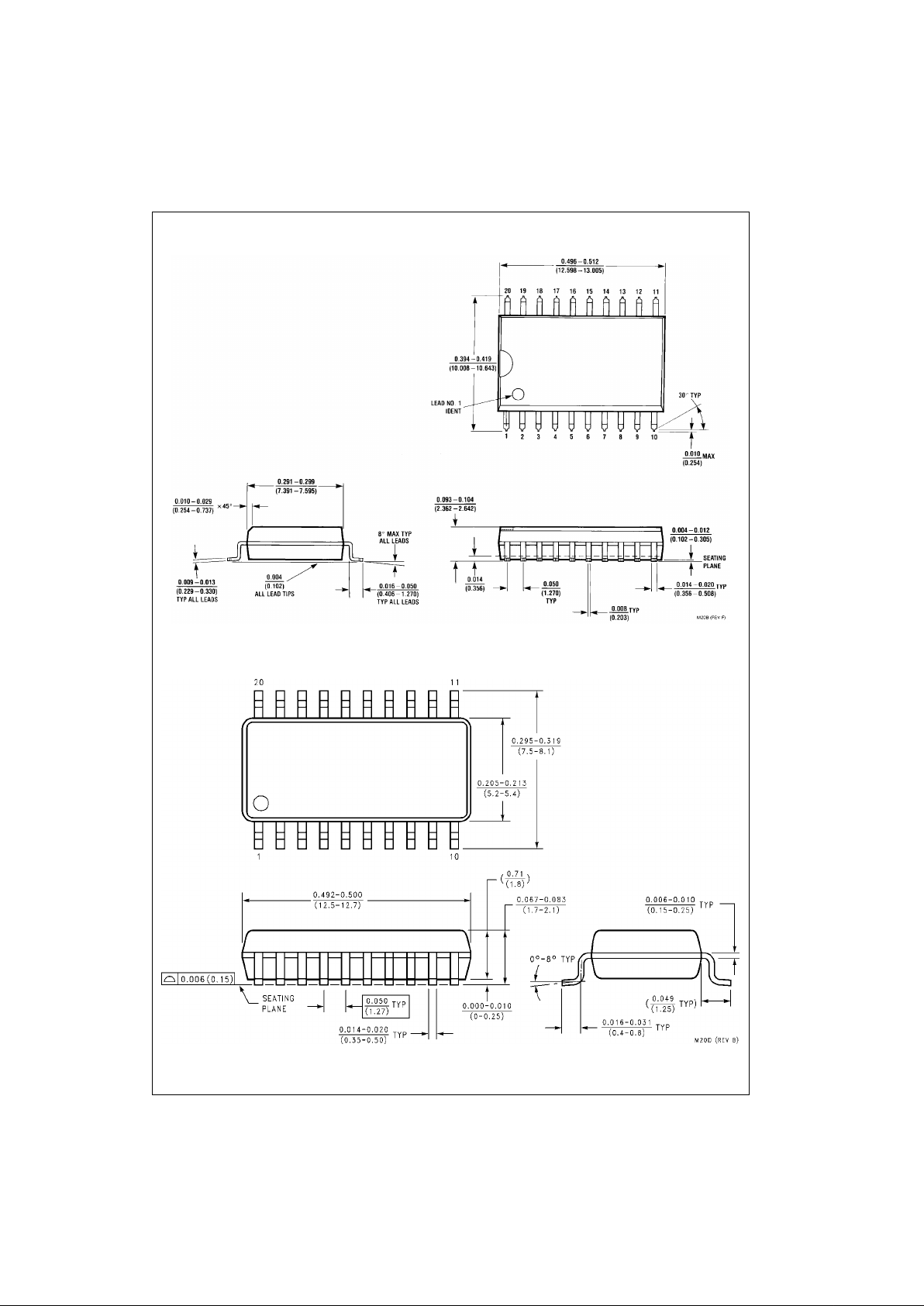
Physical Dimensions inches (millimeters) unless otherwise noted
20-Lead Small Outline Integrated Circuit (SOIC), JEDEC MS-013, 0.300” Wide
Package Number M20B
20-Lead Small Outline Package (SOP), EIAJ TYPE II, 5.3mm Wide
Package Number M20D
Page 6
www.fairchildsemi.com 6
MM74HC374
Physical Dimensions inches (millimeters) unless otherwise noted (Continued)
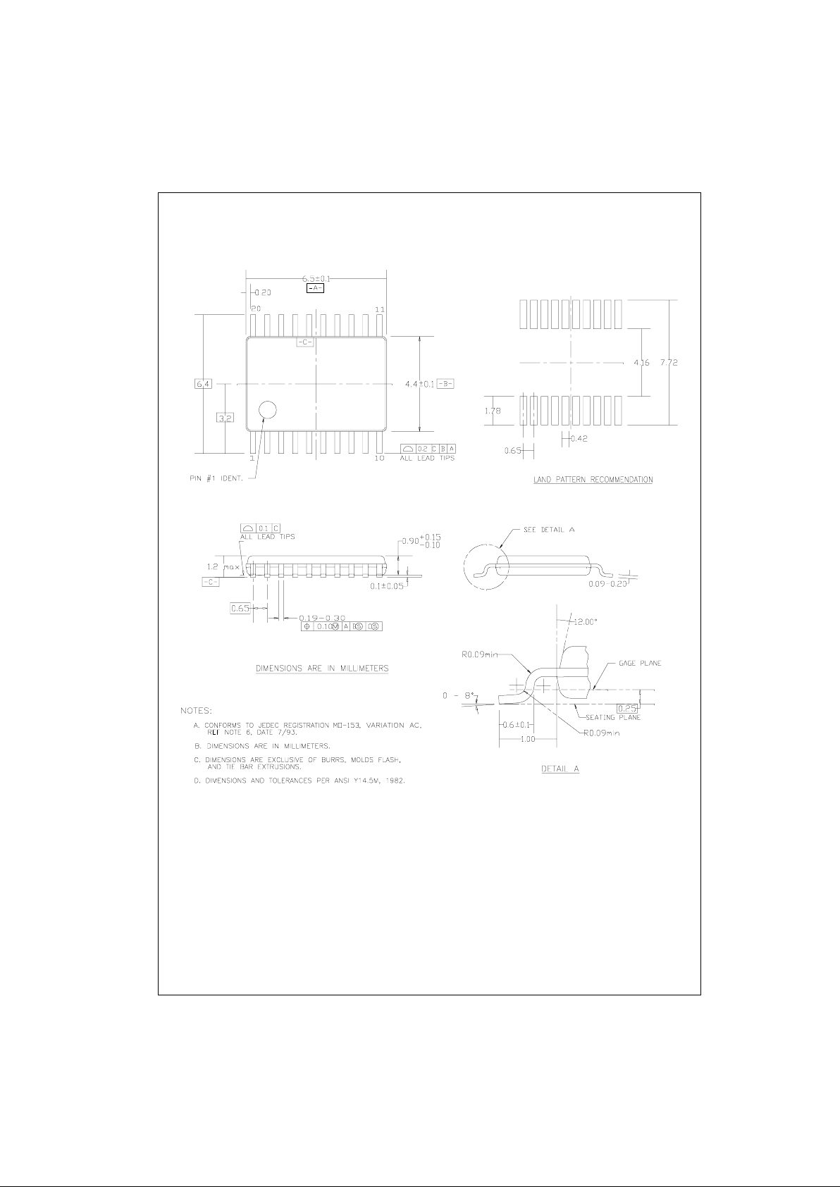
20-Lead Thin Shrink Small Outline Package (TSSOP), JEDEC MO-153, 4.4mm Wide
Package Number MTC20
Page 7

Fairchild does not assume any responsibility for use of any circuitry described, no circuit patent licenses are impli ed and Fairchild reserves the right at any time without notice to change said circuitry and specifications.
MM74HC374 3-STATE Octal D-Type Flip-Flop
LIFE SUPPORT POLICY
FAIRCHILD’S PRODUCTS ARE NOT AUTHORIZED FOR USE AS CRITICAL COMPONENTS IN LIFE SUPPORT
DEVICES OR SYSTEMS WITHOUT THE EXPRESS WRITTEN APPROVAL OF THE PRESIDENT OF FAIRCHILD
SEMICONDUCTOR CORPORATION. As used herein:
1. Life support devices or system s a re devices or syste ms
which, (a) are intended for surgical implant into the
body, or (b) support or sustain life, and (c) whose failure
to perform when properly used in accordance with
instructions for use provided in the labeling, can be reasonably expected to result in a significant injur y to the
user.
2. A critical compon ent in any com ponent of a li fe support
device or system whose failure to p erform can be r easonably expected to cause the failure of the life suppor t
device or system, or to affect its safety or effectiveness.
www.fairchildsemi.com
Physical Dimensions inches (millimeters) unless otherwise noted (Continued)
20-Lead Plastic Dual-In-Line Package (PDIP), JEDEC MS-001, 0.300” Wide
Package Number N20A
 Loading...