

Datasheet MM74HC273WM, MM74HC273MTCX, MM74HC273N, MM74HC273CW, MM74HC273WMX Datasheet (Fairchild Semiconductor)
...Page 1

September 1983
Revised February 1999
MM74HC273 Octal D-Type Flip-Flops with Clear
© 1999 Fairchild Semiconductor Corporation DS005331.prf www.fairchildsemi.com
MM74HC273
Octal D-Type Flip-Flops with Clear
General Description
The MM74HC273 edge triggered flip-flops utiliz e advance d
silicon-gate CMOS technology to implement D-type flipflops. They possess high noise immunity, low power, and
speeds comparable to low power Schottky TTL circuits.
This device contains 8 mast er-slave flip-flops with a common clock and common clear. Data on the D in put having
the specified setup and h old times is transferred to th e Q
output on the LOW-to-HIGH transitio n o f t he C LO CK inp ut.
The CLEAR input when LOW, sets all outputs to a low
state.
Each output can drive 10 low power Schottky TT L equivalent loads. The MM74HC273 is functionally as well as pin
compatible to the 74LS273 . All inputs are protected fr om
damage due to static discharge by diodes to V
CC
and
ground.
Features
■ Typical propagation delay: 18 ns
■ Wide operating voltage range
■ Low input current: 1 µA maximum
■ Low quiescent current: 80 µA (74 Series)
■ Output drive: 10 LS-TTL loads
Ordering Code:
Devices also available in Tape and Reel. Specify by appending the suffix letter “X” to the ordering code.
Connection Diagram
Pin Assignments for DIP, SOIC, SOP and TSSOP
Top View
Order Number Package Number Package Description
MM74HC273M M20B 20-Lead Small Outline Integrated Circuit (SOIC), JEDEC MS-153, 0.300” Wide
MM74HC273SJ M20D 20-Lead Small Outline Package (SOP), EIAJ TYPE II, 5.3mm Wide
MM74HC273MTC MTC20 20-Lead thin Shrink Small Outline Package (TSSOP), JEDEC MO-153, 4.4mm Wide
MM74HC273N N20A 20-Lead Plastic Dual-In-Line Package (PDIP), JEDEC MS-001, 0.300” Wide
Page 2

www.fairchildsemi.com 2
MM74HC273
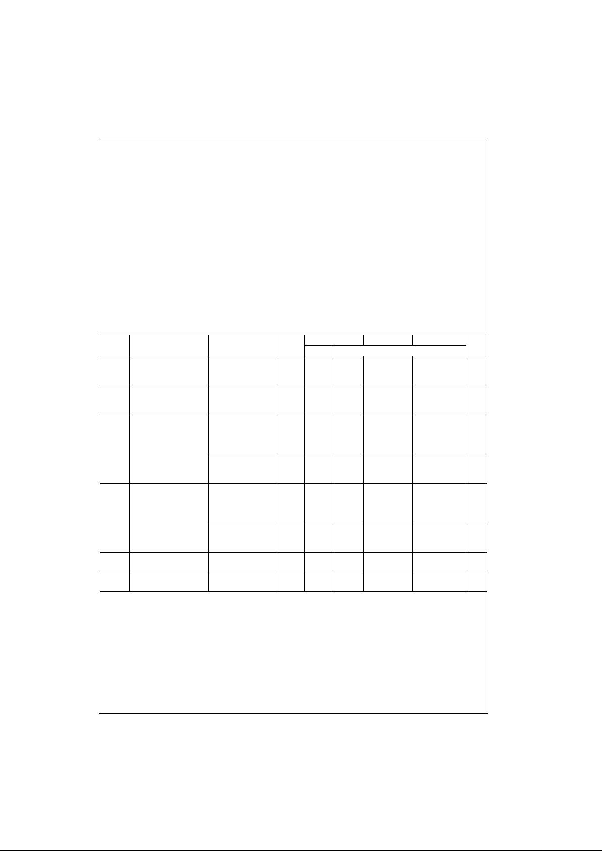
Truth Table
(Each Flip-Flop)
H = HIGH Level (Steady State)
L = LOW Level (Steady State)
X = Don’t Care
↑ = Transition from LOW-to-HIGH level
Q0 = The level of Q before the indica t ed steady state input conditions were
established
Logic Diagram
Inputs Outputs
Clear Clock D Q
LXXL
H ↑ HH
H ↑ LL
HLXQ
0
Page 3
3 www.fairchildsemi.com
MM74HC273
Absolute Maximum Ratings(Note 1)
(Note 2)
Recommended Operating
Conditions
Note 1: Absolute Maximum Rati ngs are tho se values b eyond which d am-
age to the device may occur.
Note 2: Unless otherwise specified all voltages are referenced to gro und.
Note 3: Power Dissipation temperature de rating — p lastic “N” p ackage: −
12 mW/°C from 65°C to 85°C.
DC Electrical Characteristics (Note 4)
Note 4: For a power supply o f 5V ±10% the worst case output voltages (VOH, and VOL) occur for HC at 4 .5V. Thus the 4.5V values s hould be us ed wh en
designing with this supply. Worst case V
IH
and VIL occur at V
CC
= 5.5V and 4.5V respectively. (The VIH value at 5.5V is 3.85V.) The worst case leakage cur-
rent (I
IN
, ICC, and IOZ) occur for CMOS at the higher voltage and so the 6.0V values s hould be used.
Supply Voltage (VCC) −0.5 to +7.0V
DC Input Voltage (V
IN
) −1.5 to V
CC
+1.5V
DC Output Voltage (V
OUT
) −0.5 to V
CC
+0.5V
Clamp Diode Current (I
IK
, IOK) ±20 mA
DC Output Current, per pin (I
OUT
) ±25 mA
DC V
CC
or GND Current, per pin (ICC) ±50 mA
Storage Temperature Range (T
STG
) −65°C to +150°C
Power Dissipation (P
D
)
(Note 3) 600 mW
S.O. Package only 500 mW
Lead Temperature (T
L
)
(Soldering 10 seconds) 260°C
Min Max Units
Supply Voltage (V
CC
)26V
DC Input or Output Voltage
(V
IN
, V
OUT
)0V
CC
V
Operating Temperature Range (T
A
) −40 +85 °C
Input Rise or Fall Times
(t
r
, tf) V
CC
= 2.0V 1000 ns
V
CC
= 4.5V 500 ns
V
CC
= 6.0V 400 ns
Symbol Parameter Conditions
V
CC
TA = 25°CTA = −40 to 85°CTA = −55 to 125°C
Units
Typ Guaranteed Limits
V
IH
Minimum HIGH Level 2.0V 1.5 1.5 1.5 V
Input Voltage 4.5V 3.15 3.15 3.15 V
6.0V 4.2 4.2 4.2 V
V
IL
Maximum LOW Level 2.0V 0.5 0.5 0.5 V
Input Voltage 4.5V 1.35 1.35 1.35 V
6.0V 1.8 1.8 1.8 V
V
OH
Minimum HIGH Level V
IN
= VIH or V
IL
Output Voltage |I
OUT
| ≤ 20 µA 2.0V 2.0 1.9 1.9 1.9 V
4.5V 4.5 4.4 4.4 4.4 V
6.0V 6.0 5.9 5.9 5.9 V
V
IN
= VIH or V
IL
|I
OUT
| ≤ 4.0 mA 4.5V 4.2 3.98 3.84 3.7 V
|I
OUT
| ≤ 5.2 mA 6.0V 5.7 5.48 5.34 5.2 V
V
OL
Maximum LOW Level V
IN
= VIH or V
IL
Output Voltage |I
OUT
| ≤ 20 µA 2.0V 0 0.1 0.1 0.1 V
4.5V 0 0.1 0.1 0.1 V
6.0V 0 0.1 0.1 0.1 V
V
IN
= VIH or V
IL
|I
OUT
| ≤ 4 mA 4.5V 0.2 0.26 0.33 0.4 V
|I
OUT
| ≤ 5.2 mA 6.0V 0.2 0.26 0.33 0.4 V
I
IN
Maximum Input V
IN
= VCC or GND 6.0V ±0.1 ±1.0 ±1.0 µA
Current
I
CC
Maximum Quiescent V
IN
= VCC or GND 6.0V 8 80 160 µA
Supply Current I
OUT
= 0 µA
Page 4

www.fairchildsemi.com 4
MM74HC273
AC Electrical Charac teristics
V
CC
= 5V, TA = 25°C, CL = 15 pF, tr = t
f
= 6 ns
AC Electrical Charac teristics
C
L
= 50 pF, tr = t
f
= 6 ns (unless otherwise specified)
Note 5: CPD determines the no load dynamic power cons um ption, PD = CPD V
CC
2
f + ICC VCC, and the no load dynamic current consumpt ion,
I
S
= CPDVCCf + ICC.
Symbol Parameter Conditions Typ
Guaranteed
Units
Limit
f
MAX
Maximum Operating 50 30 MHz
Frequency
t
PHL
, t
PLH
Maximum Propagation 18 27 ns
Delay, Clock to Output
t
PHL
Maximum Propagation 18 27 ns
Delay, Clear to Output
t
REM
Minimum Removal Time, 10 20 ns
Clear to Clock
t
s
Minimum Setup Time 10 20 ns
Data to Clock
t
H
Minimum Hold Time −20ns
Clock to Data
t
W
Minimum Pulse Width 10 16 ns
Clock or Clear
Symbol Parameter Conditions
V
CC
TA = 25°CTA = −40 to 85°CTA = −55 to 125°C
Units
Typ Guaranteed Limits
f
MAX
Maximum Operating 2.0V 16 5 4 3 MHz
Frequency 4.5V 74 27 21 18 MHz
6.0V 78 31 24 20 MHz
t
PHL
, t
PLH
Maximum Propagation 2.0V 38 135 170 205 ns
Delay, Clock to Output 4.5V 14 27 34 41 ns
6.0V 12 23 29 35 ns
t
PHL
Maximum Propagation 2.0V 42 135 170 205 ns
Delay, Clear to Output 4.5V 19 27 34 41 ns
6.0V 18 23 29 35 ns
t
REM
Minimum Removal Time 2.0V 0 25 32 37 ns
Clear to Clock 4.5V 0 5 6 7 ns
6.0V 0 4 5 6 ns
t
s
Minimum Setup Time 2.0V 26 100 125 150 ns
Data to Clock 4.5V 7 20 25 30 ns
6.0V 5 17 21 25 ns
t
H
Minimum Hol d Time 2.0V −15 0 0 0 ns
Clock to Data 4.5V −60 0 0 ns
6.0V −40 0 0 ns
t
W
Minimum Pulse Width 2.0V 34 80 100 120 ns
Clock or Clear 4.5V 11 16 20 24 ns
6.0V 10 14 18 20 ns
tr, t
f
Maximum Input Rise and 2.0V 1000 1000 1000 ns
Fall Time, Clock 4.5V 500 500 500 ns
6.0V 400 400 400 ns
t
THL
, t
TLH
Maximum Output Rise 2.0V 28 75 95 110 ns
and Fall Time 4.5V 11 15 19 22 ns
6.0V 9 13 16 19 ns
C
PD
Power Dissipation (per flip-flop) 45 pF
Capacitance (Note 5)
C
IN
Maximum Input 7 10 10 10 pF
Capacitance
Page 5

5 www.fairchildsemi.com
MM74HC273
Physical Dimensions inches (millimeters) unless otherwise noted
20-Lead Small Outline Integrated Circuit (SOIC), JEDEC MS-013, 0.300” Wide
Package Number M20B
20-Lead Small Outline Package (SOP), EIAJ TYPE II, 5.3mm Wide
Package Number M20D
Page 6

www.fairchildsemi.com 6
MM74HC273
Physical Dimensions inches (millimeters) unless otherwise noted (Continued)
20-Lead Thin Shrink Small Outline Package (TSSOP), JEDEC MO-153, 4.4mm Wide
Package Number MTC20
Page 7

Fairchild does not assume any responsibility for use of any circui try described, no circuit patent licenses are implied and Fairchild reserves the right at any time without notice to change said circuitry and specifications.
MM74HC273 Octal D-Type Flip-Flops with Clear
LIFE SUPPORT POLICY
FAIRCHILD’S PRODUCTS ARE NOT AUTHORIZED FOR USE AS CRITICAL COMPONENTS IN LIFE SUPPORT
DEVICES OR SYSTEMS WITHOUT THE EXPRESS WRITTEN APPROVAL OF THE PRESIDENT OF FAIRCHILD
SEMICONDUCTOR CORPORATION. As used herein:
1. Life support devices or system s a re devices or syste ms
which, (a) are intended for surgical implant into the
body, or (b) support or sustain life, and (c) whose failure
to perform when properly used in accordance with
instructions for use provided in the labeling, can be reasonably expected to result in a significant injur y to the
user.
2. A critical compon ent in any com ponent of a li fe support
device or system whose failure to p erform can be r easonably expected to cause the failure of the life suppor t
device or system, or to affect its safety or effectiveness.
www.fairchildsemi.com
Physical Dimensions inches (millimeters) unless otherwise noted (Continued)
20-Lead Plastic Dual-In-Line Package (PDIP), JEDEC MS-001, 0.300” Wide
Package Number N20A
 Loading...