

Datasheet MM74HC259M, MM74HC259N, MM74HC259MTC, MM74HC259MTCX, MM74HC259SJX Datasheet (Fairchild Semiconductor)
...Page 1
September 1983
Revised February 1999
MM74HC259 8-Bit Addressable Latch/3-to-8 Line Decoder
© 1999 Fairchild Semiconductor Corporation DS005006.prf www.fairchildsemi.com
MM74HC259
8-Bit Addressable Latch/3-to-8 Line Decoder
General Description
The MM74HC259 device utilizes advanced silicon-gate
CMOS technology to implement an 8-bit addressable latch,
designed for general purpose storage applications in digital
systems.
The MM74HC259 has a single data in put (D), 8 latch out-
puts (Q1–Q8), 3 addres s inputs (A, B, and C), a co mmon
enable input (G
), and a common CLEAR input. To operate
this device as an addres sable latch, d ata is held on th e D
input, and the add ress of the la tch i nto whic h th e dat a is to
be entered is held on the A, B, and C inputs. When
ENABLE is taken LOW the data flows through to the
addressed ou tpu t. The data i s stor ed wh en ENABL E tr ansi tions from LOW-to-HIGH. All unaddressed latches will
remain unaffected. With enable in the HIGH state the
device is deselected, and all latches remain in their previous state, unaffected by changes on the data or a ddress
inputs. To eliminate the possibility of entering erroneous
data into the latches, the enable should be held HIGH
(inactive) while the address lines are changing.
If enable is held HIGH and CLEAR is taken LOW all eight
latches are cleared to a LOW state. If enable is LOW all
latches except the addressed latch will be cleared. The
addressed latch will instead follow the D input, effectively
implementing a 3-to-8 line decoder.
All inputs are protected from damage due to static discharge by diodes to V
CC
and ground.
Features
■ Typical propagation delay: 18 ns
■ Wide supply range: 2–6V
■ Low input current: 1 µA maximum
■ Low quiescent current: 80 µA maximum (74HC Series)
Ordering Code:
Devices also availab le in Tape and Reel. Specify by appending th e s uffix let t er “X” to the ordering cod e.
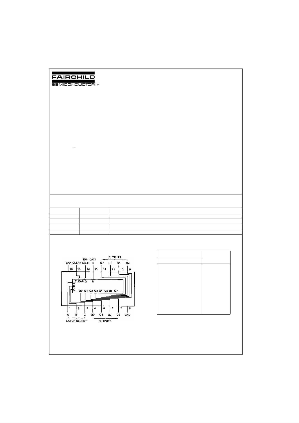
Connection Diagram
Pin Assignments f or DIP, SOIC, SOP and TSSOP
Top View
Latch Selection Table
H = HIGH level, L = LOW level
D = the level at the d at a input
Q
i0
the level of Qi (i = 0, 1...7, as appropriate)
before the indicate d s te ady-state input
conditions were est ablished.
Order Number Package Number Package Description
MM74HC259M M16A 16-Lead Small Outline Integrated Circuit (SOIC), JEDEC MS-120, 0.150” Narrow
MM74HC259SJ M16D 16-Lead Small Outline Package (SOP), EIAJ TYPE II, 5.3mm Wide
MM74HC259MTC MTC16 16-Lead Thin Shrink Small Outline Package (TSSOP), JEDEC MO-153, 4.4mm Wide
MM74HC259N N16E 16-Lead Plastic Dual-In-Line Package (PDIP), JEDEC MS-001, 0.300” Wide
Select Inputs Latch
C B A Addressed
LLL 0
LLH 1
LHL 2
LHH 3
HLL 4
HLH 5
HHL 6
HHH 7
Page 2
www.fairchildsemi.com 2
MM74HC259
Truth Table
Logic Diagram
Inputs Outputs of Each
Addressed Other Function
Clear G
Latch Output
HL D Q
i0
Addressable Latch
HH Q
i0
Q
i0
Memory
L L D L 8-Line Decoder
L H L L Clear
Page 3
3 www.fairchildsemi.com
MM74HC259
Absolute Maximum Ratings(Note 1)
(Note 2)
Recommended Operating
Conditions
Note 1: Absolute Maximum Ra tings are those valu es beyond w hich dam-
age to the device may occur.
Note 2: Unless otherwise specified all voltages are referenced to ground.
Note 3: Power Dissipation te mperature d erating — pl astic “N” pa ckage: −
12 mW/°C from 65°C to 85°C
DC Electrical Characteristics (Note 4)
Note 4: For a powe r supply o f 5V ±10% the worst case output voltages (VOH, and VOL) occur for HC at 4.5V. Thus the 4. 5V valu es shou ld be u sed when
designing with this supply. Worst case V
IH
and VIL occur at VCC=5.5V and 4.5V respectively. (The VIH value at 5.5V is 3. 85V.) The worst case leak ag e cur ren t
(I
IN
, ICC, and IOZ) occur for CMOS at the higher voltage and s o t he 6.0V values should be used.
Supply Voltage (VCC) −0.5 to +7.0V
DC Input Voltage (V
IN
) −1.5 to VCC+1.5V
DC Output Voltage (V
OUT
) −0.5 to VCC+0.5V
Clamp Diode Current (I
IK
, IOK) ±20 mA
DC Output Current, per pin (I
OUT
) ±25 mA
DC V
CC
or GND Current, per pin (ICC) ±50 mA
Storage Temperature Range (T
STG
) −65°C to +150°C
Power Dissipation (P
D
)
(Note 3) 600 mW
S.O. Package only 500 mW
Lead Temperature (T
L
)
(Soldering 10 seconds) 260°C
Min Max Units
Supply Voltage (V
CC
)26V
DC Input or Output Voltage 0 V
CC
V
(V
IN
, V
OUT
)
Operating Temperature Range (T
A
) −40 +85 °C
Input Rise or Fall Times
(t
r
, tf) V
CC
= 2.0V 1000 ns
V
CC
= 4.5V 500 ns
V
CC
= 6.0V 400 ns
Symbol Parameter Conditions
V
CC
TA= 25°CTA = −40 to 85°CTA = −55 to 125°C
Units
Typ Guaranteed Limits
V
IH
Minimum HIGH Level 2.0V 1.5 1.5 1.5 V
Input Voltage 4.5V 3.15 3.15 3.15 V
6.0V 4.2 4.2 4.2 V
V
IL
Maximum LOW Level 2.0V 0.5 0.5 0.5 V
Input Voltage 4.5V 1.35 1.35 1.35 V
6.0V 1.8 1.8 1.8 V
V
OH
Minimum HIGH Level V
IN
= VIH or V
IL
Output Voltage |I
OUT
| ≤ 20 µA 2.0V 2.0 1.9 1.9 1.9 V
4.5V 4.5 4.4 4.4 4.4 V
6.0V 6.0 5.9 5.9 5.9 V
V
IN
= VIH or V
IL
|I
OUT
| ≤ 4.0 mA 4.5V 4.2 3.98 3.84 3.7 V
|I
OUT
| ≤ 5.2 mA 6.0V 5.7 5.48 5.34 5.2 V
V
OL
Maximum LOW Level V
IN
= VIH or V
IL
Output Voltage |I
OUT
| ≤ 20 µA 2.0V 0 0.1 0.1 0.1 V
4.5V 0 0.1 0.1 0.1 V
6.0V 0 0.1 0.1 0.1 V
V
IN
= VIH or V
IL
|I
OUT
| ≤ 4.0 mA 4.5V 0.2 0.26 0.33 0.4 V
|I
OUT
| ≤ 5.2 mA 6.0V 0.2 0.26 0.33 0.4 V
I
IN
Maximum Input V
IN
= VCC or GND 6 .0V ±0.1 ±1.0 ±1.0 µA
Current
I
CC
Maximum Quiescent V
IN
= VCC or GND 6.0V 8.0 80 160 µA
Supply Current I
OUT
= 0 µA
Page 4

www.fairchildsemi.com 4
MM74HC259
AC Electrical Characteristics
(V
CC
= 5.0V, TA = 25°C, tr = tf = 6 ns, C
L
= 15 pF unless otherwise specified.)
AC Electrical Characteristics
t
r
= tf = 6 ns, CL = 50 pF, V
CC
= 2.0V – 6.0V
Note 5: CPD determines the no lo ad dynamic power con s um ption, PD = CPD V
CC
2
f + ICC VCC, and the no load dynam ic c urrent consumption ,
I
S
= CPDs VCCsf + ICC.
Symbol Parameter Conditions Typ
Guaranteed
Units
Limit
t
PHL
, t
PLH
Maximum Propagation Delay 18 32 ns
Data to Output
t
PHL
, t
PLH
Maximum Propagation Delay 20 38 ns
Select to Output
t
PHL
, t
PLH
Maximum Propagation Delay 20 35 ns
Enable to Output
t
PHL
Maximum Propagation Delay 17 27 ns
Clear to Output
t
W
Minimum Enable Pulse Width 10 16 ns
t
W
Minimum Clear Pulse Width 10 16 ns
tr, t
f
Maximum Input Rise and Fall Time 500 ns
t
s
Minimum Setup Time Select or 15 20 ns
Data to Enable
t
H
Minimum Hol d Time Data or −20ns
Address to Enable
Symbol Parameter Conditions
V
CC
TA = 25°CTA = −40 to 85°CTA = −55 to 125°C
Units
Typ Guaranteed Limits
t
PHL
, t
PLH
Maximum Propagation Delay 2.0V 60 180 225 250 ns
Data to Output 4.5V 19 37 46 52 ns
6.0V 17 32 40 45 ns
t
PHL
, t
PLH
Maximum Propagation Delay 2.0V 72 220 275 310 ns
Select to Output 4.5V 21 43 54 60 ns
6.0V 18 37 46 52 ns
t
PHL
, t
PLH
Maximum Propagation Delay 2.0V 65 200 250 280 ns
Enable to Output 4.5V 27 40 50 58 ns
6.0V 23 35 44 50 ns
t
PHL
Maximum Propagation Delay 2.0V 50 150 190 210 ns
Clear to Output 4.5V 18 31 39 44 ns
6.0V 16 26 32 37 ns
t
W
Minimum Pulse Width 2.0V 80 100 120 ns
Clear or Enable 4.5V 16 20 24 ns
6.0V 14 18 20 ns
t
s
Minimum Setup Time Address 2.0V 100 125 150 ns
or Data to Enable 4.5V 20 25 28 ns
6.0V 15 19 25 ns
t
H
Minimum Hold Time Address 2.0V −10 0 0 0 ns
or Data to Enable 4.5V −20 0 0 ns
6.0V −20 0 0 ns
t
TLH
, t
THL
Maximum Output Rise 2.0V 30 75 95 110 ns
and Fall Time 4.5V 8 15 19 22 ns
6.0V 7 13 16 19 ns
C
IN
Input Capacitance 5 10 10 10 pF
C
PD
Power Dissipation (per package) 80 pF
Capacitance (Note 5)
Page 5

5 www.fairchildsemi.com
MM74HC259
Physical Dimensions inches (millimeters) unless otherwise noted
16-Lead Small Outline Integrated Circuit (SOIC), JEDEC MS-012, 0.150” Narrow
Package Number M16A
16-Lead Small Outline Package (SOP), EIAJ TYPE II, 5.3mm Wide
Package Number M16D
Page 6

www.fairchildsemi.com 6
MM74HC259
Physical Dimensions inches (millimeters) unless otherwise noted (Continued)
16-Lead Thin Shrink Small Outline Package (TSSOP), JEDEC MO-153, 4.4mm Wide
Package Number MTC16
Page 7

Fairchild does not assume any responsibility for use of any circuitry described, no circuit patent licenses are implied and Fairchild reserves the right at any time without notice to change said circuitry and specifications.
MM74HC259 8-Bit Addressable Latch/3-to-8 Line Decoder
LIFE SUPPORT POLICY
FAIRCHILD’S PRODUCTS ARE NOT AUTHORIZED FOR USE AS CRITICAL COMPONENTS IN LIFE SUPPORT
DEVICES OR SYSTEMS WITHOUT THE EXPRESS WRITTEN APPROVAL OF THE PRESIDENT OF FAIRCHILD
SEMICONDUCTOR CORPORATION. As used herein:
1. Life support devices or systems are dev ic es or syste ms
which, (a) are intended for surgical implant into the
body, or (b) support or sustain life, and (c) whose failure
to perform when properly used in accordance with
instructions for use provided i n the labe li ng, can be re asonably expected to result in a significant injury to the
user.
2. A critical componen t in any com ponent o f a l ife supp ort
device or system whose failu re to perform can b e reasonably expected to c ause th e fa i lure of the li fe s upp or t
device or system, or to affect its safety or effectiveness.
www.fairchildsemi.com
Physical Dimensions inches (millimeters) unless otherwise noted (Continued)
16-Lead Plastic Dual-In-Line Package (PDIP), JEDEC MS-001, 0.300” Wide
Package Number N16E
 Loading...