

Datasheet MM74HC245AWMX, MM74HC245ASJX, MM74HC245ACW, MM74HC245AMTC, MM74HC245AMTCX Datasheet (Fairchild Semiconductor)
...Page 1
September 1983
Revised February 1999
MM74HC245A Octal 3-STATE Transceiver
© 1999 Fairchild Semiconductor Corporation DS005165.prf www.fairchildsemi.com
MM74HC245A
Octal 3-STATE Transceiver
General Description
The MM74HC245A 3-STATE bidirectional buffer utilizes
advanced silicon-gate CMOS technology, and is intended
for two-way asynchronous communication between data
buses. It has high drive current out puts which enable high
speed operation even when driving large bus capacitances. This circuit possesses the low power co nsumption
and high noise immunity usually associated with CMOS circuitry, yet has speeds comparable to low power Schottky
TTL circuits.
This device has an active LOW enable input G
and a direction control input, DIR. When DIR is HIGH, data flows from
the A inputs to the B outputs. When DIR is LOW, data flows
from the B inputs to the A outputs. The MM74HC245A
transfers true data from one bus to the other.
This device can drive up to 15 LS-TTL Loads, and does not
have Schmitt trigg er inputs. All inputs are protected from
damage due to static discharge by diodes to V
CC
and
ground.
Features
■ Typical propagation delay: 13 ns
■ Wide power supply range: 2–6V
■ Low quiescent current: 80 µA maximum (74 HC)
■ 3-STATE outputs for connection to bus oriented systems
■ High output drive: 6 mA (minimum)
■ Same as the 645
Ordering Code:
Devices also availab le in Tape and Reel. Specify by appending th e s uffix let t er “X” to the ordering cod e.
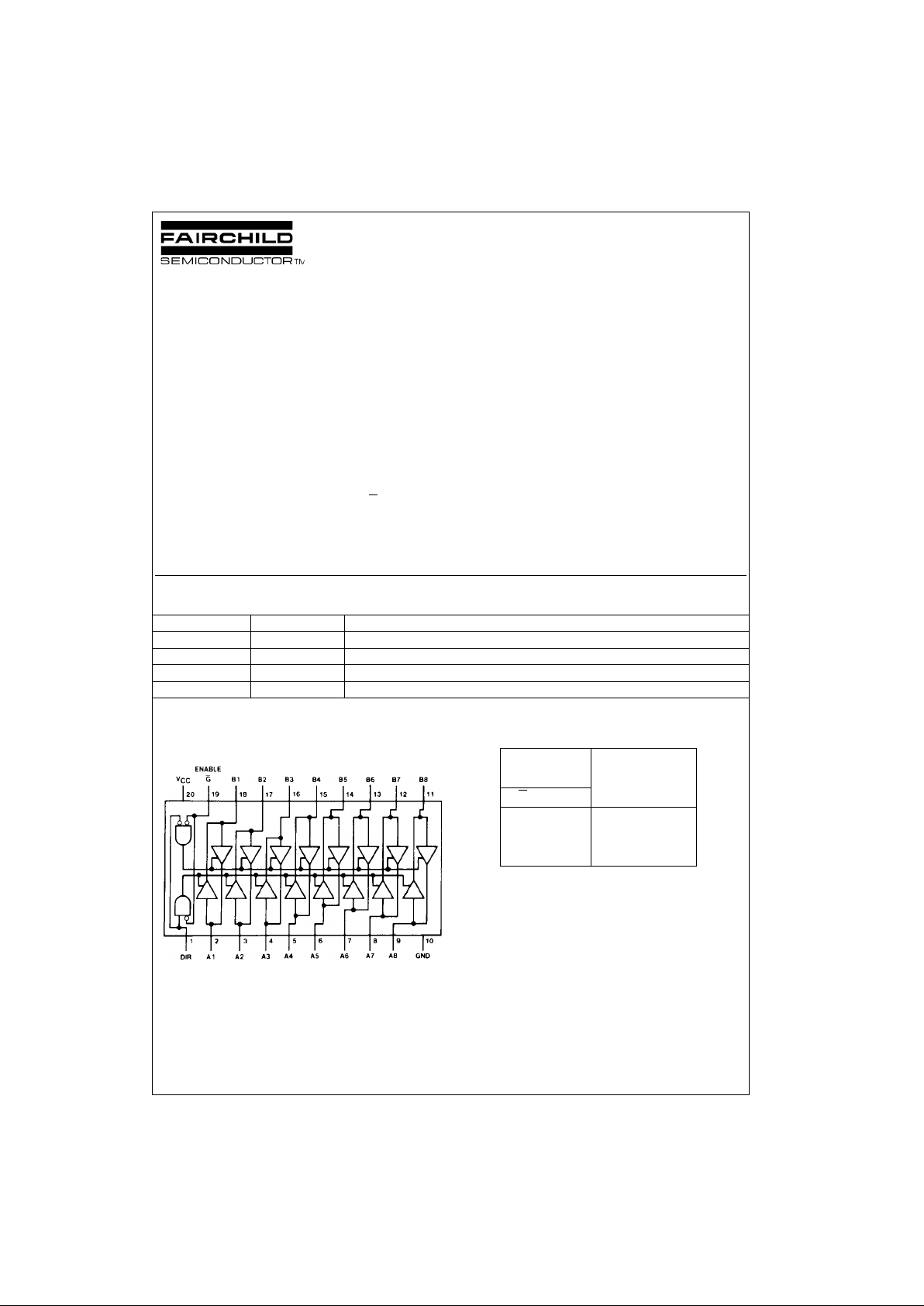
Connection Diagram
Pin Assignments f or DIP, SOIC, SOP and TSSOP
Top View
Truth Table
H = HIGH Level
L = LOW Level
X = Irrelevant
Order Number Package Number Package Description
MM74HC245AWM M20B 20-Lead Small Outline Integrated Circuit (SOIC), JEDEC MS-013, 0.300” Wide
MM74HC245ASJ M20D 20-Lead Small Outline Package (SOP), EIAJ TYPE II, 5.3mm Wide
MM74HC245AMTC MTC20 20-Lead Thin Shrink Small Outline Package (TSSOP), JEDEC MO-153, 4.4mm Wide
MM74HC245AN N20A 20-Lead Plastic Dual-In-Line Package (PDIP), JEDEC MS-001, 0.300” Wide
Control
Inputs Operation
G
DIR
L L B data to A bus
L H A data to B bus
HX Isolation
Page 2
www.fairchildsemi.com 2
MM74HC245A
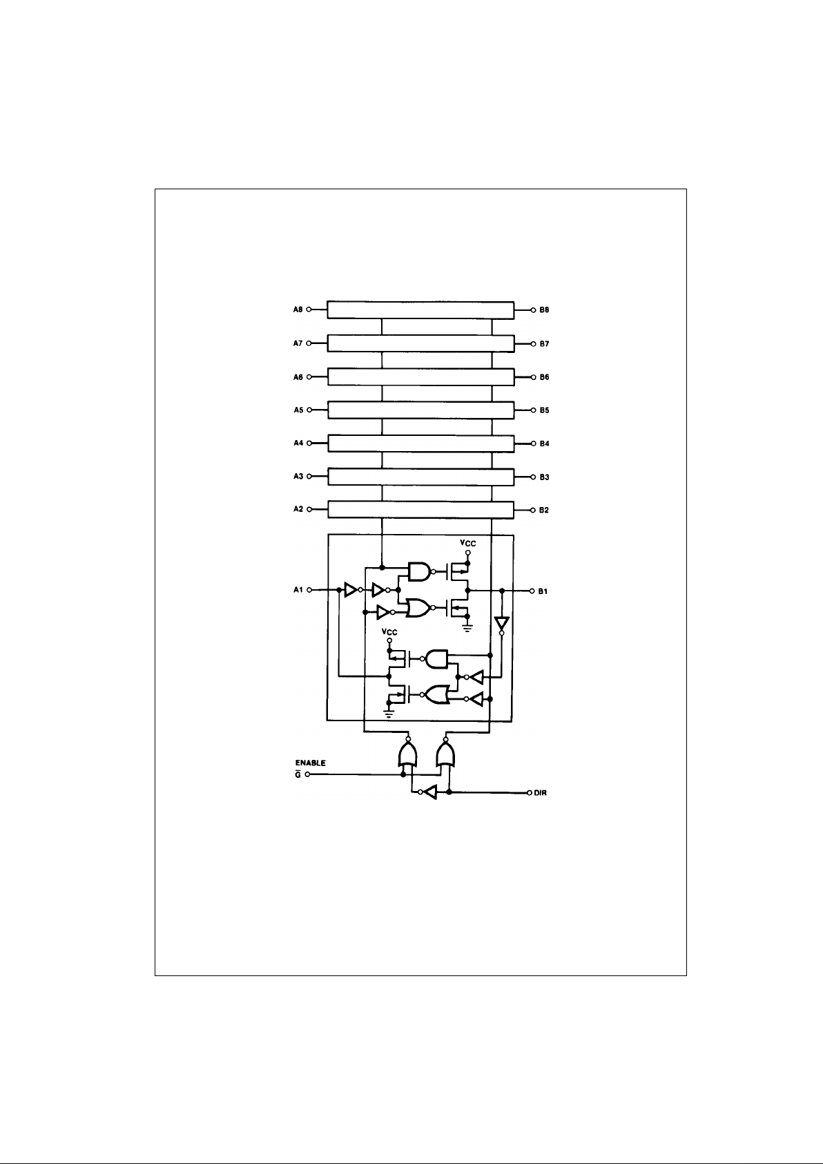
Logic Diagram
Page 3
3 www.fairchildsemi.com
MM74HC245A
Absolute Maximum Ratings(Note 1)
(Note 2)
Recommended Operating
Conditions
Note 1: Maximum Ratings are those values beyond which damage to the
device may occur.
Note 2: Unless otherwise specified all voltages are referenced to ground.
Note 3: Power Dissipation te mperature d erating — pl astic “N” pa ckage: −
12 mW/°C from 65°C to 85°C.
DC Electrical Characteristics (Note 4)
Note 4: For a powe r supply o f 5V ±10% the worst case output voltages (VOH, and VOL) occur for HC at 4.5V. Thus the 4. 5V valu es shou ld be u sed when
designing with this supply. Worst case V
IH
and VIL occur at V
CC
= 5.5V and 4.5V respectively. (The VIH value at 5.5V is 3 .8 5V.) The worst c as e leakage cur-
rent (I
IN
, ICC, and IOZ) occur for CMOS at the higher voltage and so th e 6. 0V values should be used.
Supply Voltage (VCC) −0.5 to +7.0V
DC Input Voltage DIR and G
pins (VIN) −1.5 to V
CC
+1.5V
DC Input/Output Voltage (V
IN
, V
OUT
) −0.5 to V
CC
+0.5V
Clamp Diode Current (I
CD
) ±20 mA
DC Output Current, per pin (I
OUT
) ±35 mA
DC V
CC
or GND Current, per pin (ICC) ±70 mA
Storage Temperature Range (T
STG
) −65°C to +150°C
Power Dissipation (P
D
)
(Note 3) 600 mW
S.O. Package only 500 mW
Lead Temperature (T
L
)
(Soldering 10 second s) 260°C
Min Max Units
Supply Voltage (V
CC
)26V
DC Input or Output Voltage
(V
IN
, V
OUT
)0V
CC
V
Operating Temperature Range (T
A
) −40 +85 °C
Input Rise/Fall Times
(t
r
, tf) V
CC
= 2.0V 1000 ns
V
CC
= 4.5V 500 ns
V
CC
= 6.0V 400 ns
Symbol Parameter Conditions
V
CC
TA = 25°CTA = −40 to 85°CTA = −55 to 125°C
Units
Typ Guaranteed Limits
V
IH
Minimum HIGH Level Input 2.0V 1.5 1.5 1.5 V
Voltage 4.5V 3.15 3.15 3.15 V
6.0V 4.2 4.2 4.2 V
V
IL
Maximum LOW Level Input 2.0V 0.5 0.5 0.5 V
Voltage 4.5V 1.35 1.35 1.35 V
6.0V 1.8 1.8 1.8 V
V
OH
Minimum HIGH Level Output V
IN
= VIH or V
IL
Voltage |I
OUT
| ≤ 20 µA 2.0V 2.0 1.9 1.9 1.9 V
4.5V 4.5 4.4 4.4 4.4 V
6.0V 6.0 5.9 5.9 5.9 V
V
IN
= VIH or V
IL
|I
OUT
| ≤ 6.0 mA 4.5V 4.2 3.98 3.84 3.7 V
|I
OUT
| ≤ 7.8 mA 6.0V 5.7 5.48 5.34 5.2 V
V
OL
Maximum LOW Level Output V
IN
= VIH or V
IL
Voltage |I
OUT
| ≤ 20 µA 2.0V 0 0.1 0.1 0.1 V
4.5V 0 0.1 0.1 0.1 V
6.0V 0 0.1 0.1 0.1 V
V
IN
= VIH or V
IL
|I
OUT
| ≤ 6.0 mA 4.5V 0.2 0.26 0.33 0.4 V
|I
OUT
| ≤ 7.8 mA 6.0V 0.2 0.26 0.33 0.4 V
I
IN
Input Leakage V
IN
= VCC to GND 6.0V ±0.1 ±1.0 ±1.0 µA
Current (G and DIR)
I
OZ
Maximum 3-STATE Output V
OUT
= VCC or GND 6.0V ±0.5 ±5.0 ±10 µA
Leakage Current
Enable G = V
IH
I
CC
Maximum Quiescent Supply V
IN
= VCC or GND 6.0V 8.0 80 160 µA
Current I
OUT
= 0 µA
Page 4

www.fairchildsemi.com 4
MM74HC245A
AC Electrical Characteristics
V
CC
= 5V, T
A
= 25°C, t
r
= t
f
= 6ns
AC Electrical Characteristics
V
CC
= 2.0V to 6.0V, CL = 50 pF, tr = t
f
= 6ns (unless otherwise specified)
Note 5: CPD determines the no load dynamic power consumption, PD=CPD V
CC
2
f+ICC VCC, and the no load dynamic current consumption, IS=CPDVCCf+ICC.
Symbol Parameter Conditions Typ
Guaranteed
Units
Limit
t
PHL
, t
PLH
Maximum Propagation Delay CL = 45 pF 12 17 ns
t
PZH
, t
PZL
Maximum Output Enable RL = 1 kΩ 24 35 ns
Time CL = 45 pF
t
PHZ
, t
PLZ
Maximum Output Disable RL = 1 kΩ 18 25 ns
Time CL = 5 pF
Symbol Parameter Conditions
V
CC
TA = 25°CTA = −40 to 85°CTA = −55 to 125°C
Units
Typ Guaranteed Limits
t
PHL
, Maximum Propagation CL = 50 pF 2.0V 31 90 113 135 ns
t
PLH
Delay CL = 150 pF 2.0V 41 96 116 128 ns
CL = 50 pF 4.5V 13 18 23 27 ns
CL = 150 pF 4.5V 17 22 28 33 ns
CL = 50 pF 6.0V 11 15 19 23 ns
CL = 150 pF 6.0V 14 19 23 28 ns
t
PZH
, Maximum Output Enable RL = 1 kΩ
t
PZL
Time CL = 50 pF 2.0V 71 190 240 285 ns
CL = 150 pF 2.0V 81 240 300 360 ns
CL = 50 pF 4.5V 26 38 48 57 ns
CL = 150 pF 4.5V 31 48 60 72 ns
CL = 50 pF 6.0V 21 32 41 48 ns
CL = 150 pF 6.0V 25 41 51 61 ns
t
PHZ
, Maximum Output Disable RL = 1 kΩ 2.0V 39 135 169 203 ns
t
PLZ
Time CL = 50 pF 4.5V 20 27 34 41 ns
6.0V 18 23 29 34 ns
t
TLH
, t
THL
Output Rise and Fall Time CL=50 pF 2.0V 20 60 75 90 ns
4.5V 6 12 15 18 ns
6.0V 5 10 13 15 ns
C
PD
Power Dissipation G = V
IL
50 pF
Capacitance (Note 5)
G = V
IH
5pF
C
IN
Maximum Input Capacitance 5 10 10 10 pF
C
IN/OUT
Maximum Input/Output 15 20 20 20 pF
Capacitance, A or B
Page 5

5 www.fairchildsemi.com
MM74HC245A
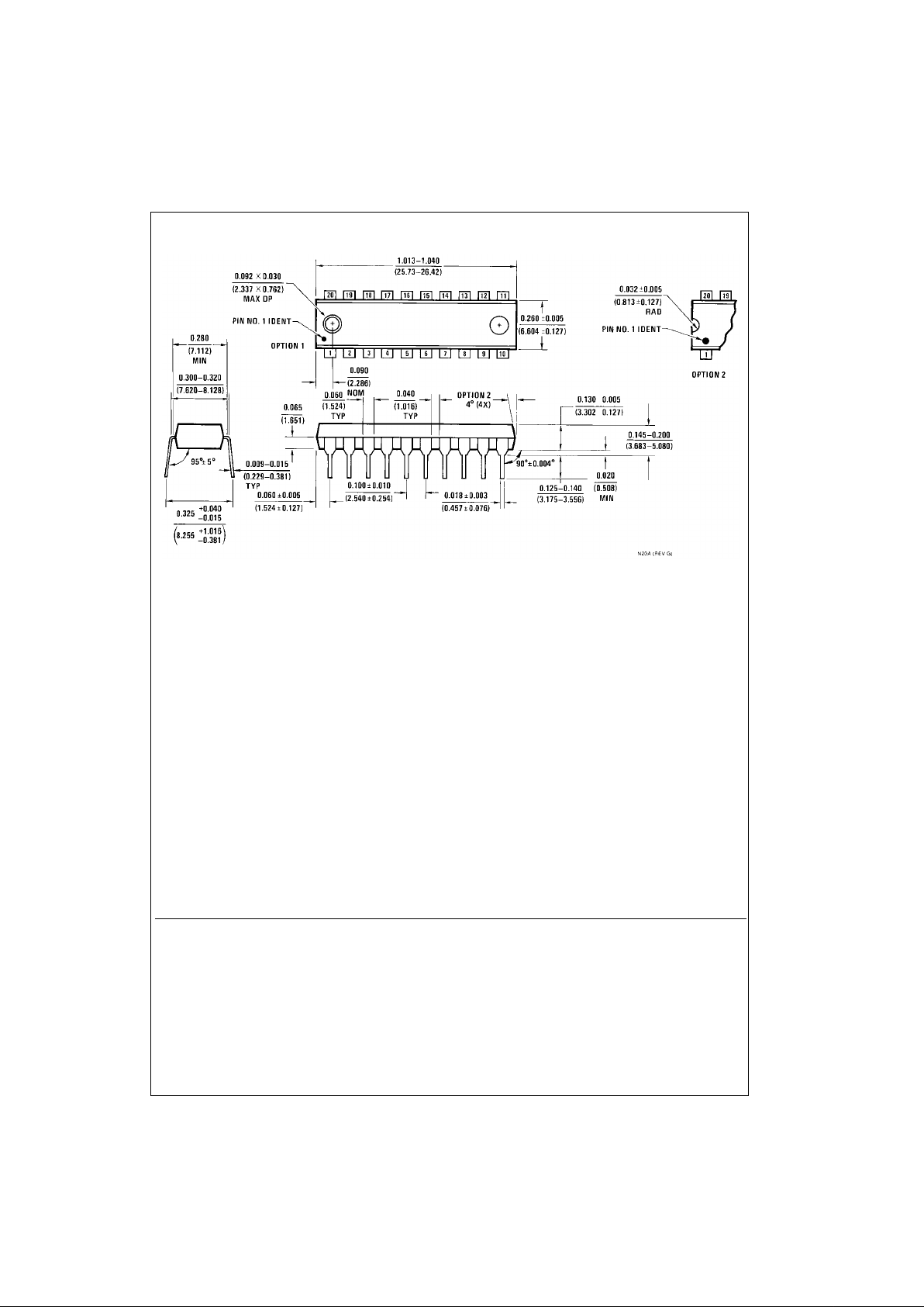
Physical Dimensions inches (millimeters) unless otherwise noted
20-Lead Small Outline Integrated Circuit (SOIC), JEDEC MS-013, 0.300” Wide
Package Number M20B
20-Lead Small Outline Package (SOP), EIAJ TYPE II, 5.3mm Wide
Package Number M20D
Page 6

www.fairchildsemi.com 6
MM74HC245A
Physical Dimensions inches (millimeters) unless otherwise noted (Continued)
20-Lead Thin Shrink Small Outline Package (TSSOP), JEDEC MO-153, 4.4mm Wide
Package Number MTC20
Page 7
Fairchild does not assume any responsibility for use of any circuitry described, no circuit patent licenses are implied and Fairchild reserves the right at any time without notice to change said circuitry and specifications.
MM74HC245A Octal 3-STATE Transceiver
LIFE SUPPORT POLICY
FAIRCHILD’S PRODUCTS ARE NOT AUTHORIZED FOR USE AS CRITICAL COMPONENTS IN LIFE SUPPORT
DEVICES OR SYSTEMS WITHOUT THE EXPRESS WRITTEN APPROVAL OF THE PRESIDENT OF FAIRCHILD
SEMICONDUCTOR CORPORATION. As used herein:
1. Life support devices or systems are dev ic es or syste ms
which, (a) are intended for surgical implant into the
body, or (b) support or sustain life, and (c) whose failure
to perform when properly used in accordance with
instructions for use provided i n the labe li ng, can be re asonably expected to result in a significant injury to the
user.
2. A critical componen t in any com ponent o f a l ife supp ort
device or system whose failu re to perform can b e reasonably expected to c ause th e fa i lure of the li fe s upp or t
device or system, or to affect its safety or effectiveness.
www.fairchildsemi.com
Physical Dimensions inches (millimeters) unless otherwise noted (Continued)
20-Lead Plastic Dual-In-Line Package (PDIP), JEDEC MS-001, 0.300” Wide
Package Number N20A
 Loading...