

Datasheet MM74HC244N, MM74HC244WM, MM74HC244MTC, MM74HC244SJX, MM74HC244SJ Datasheet (Fairchild Semiconductor)
...Page 1
© 2000 Fairchild Semiconductor Corporation DS005327 www.fairchildsemi.com
September 1983
Revised August 2000
MM74HC244 Octal 3-STATE Buffer
MM74HC244
Octal 3-STATE Buffer
General Description
The MM74HC244 is a non-inverting buffer and has two
active low enables (1G and 2G); each enable independently controls 4 buffers. This device does not have
Schmitt trigger inputs.
These 3-STATE buffers utilize advanced silicon-gate
CMOS technology and are general purpose high speed
non-inverting buffers. The y possess h igh dri ve cur rent ou tputs which enable high spe ed o per ati o n eve n whe n dr i ving
large bus capacitances. These circuits achieve speeds
comparable to low power Schottky devices, while retaining
the advantage of CMOS circuitry, i.e., high noise immu nity,
and low power consumption. All three devices have a
fanout of 15 LS-TTL equivalent inputs.
All inputs are protected from damage due to static discharge by diodes to V
CC
and ground.
Features
■ Typical propagation delay: 14 ns
■ 3-STATE outputs for connection to system buses
■ Wide power supply range: 2–6V
■ Low quiescent supply current: 80
µA
■ Output current: 6 mA
Ordering Code:
Devices also availab le in Tape and Reel. Specify by appending th e s uffix let t er “X” to the ordering code.
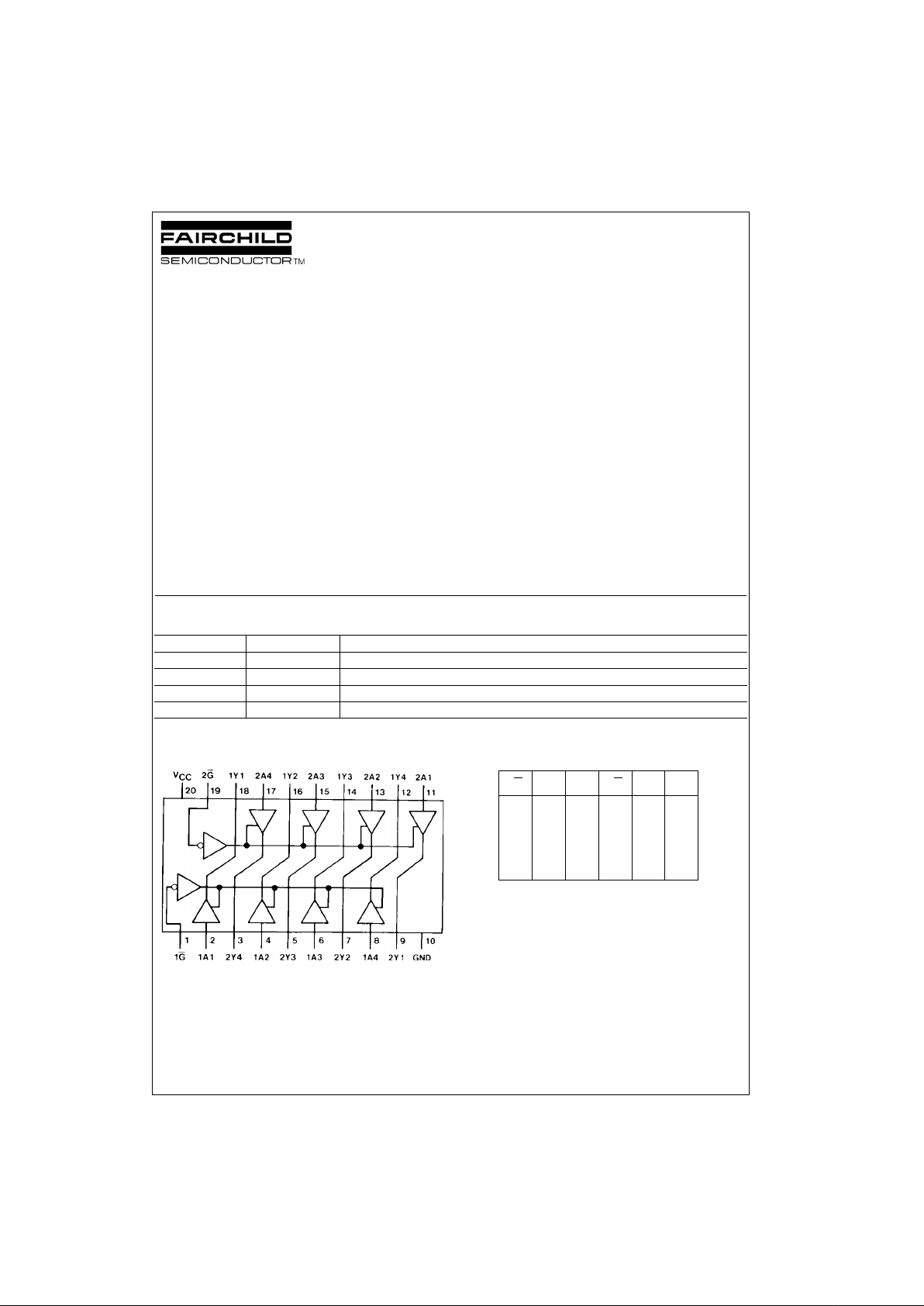
Connection Diagram
Top View
Truth Table
H = HIGH Level
L = LOW Level
Z = High Impedance
Order Number Package Number Package Description
MM74HC244WM M20B 20-Lead Small Outline Integrated Circuit (SOIC), JEDEC MS-013, 0.300” Wide
MM74HC244SJ M20D 20-Lead Small Outline Package (SOP), EIAJ TYPE II, 5.3mm Wide
MM74HC244MTC MTC20 20-Lead Thin Shrink Small Outline Package (TSSOP), JEDEC MO-153, 4.4mm Wide
MM74HC244N N20A 20-Lead Plastic Dual-In-Line Package (PDIP), JEDEC MS-001, 0.300” Wide
1G 1A 1Y 2G 2A 2Y
LLLLLL
LHHLHH
HLZHLZ
HHZHHZ
Page 2
www.fairchildsemi.com 2
MM74HC244
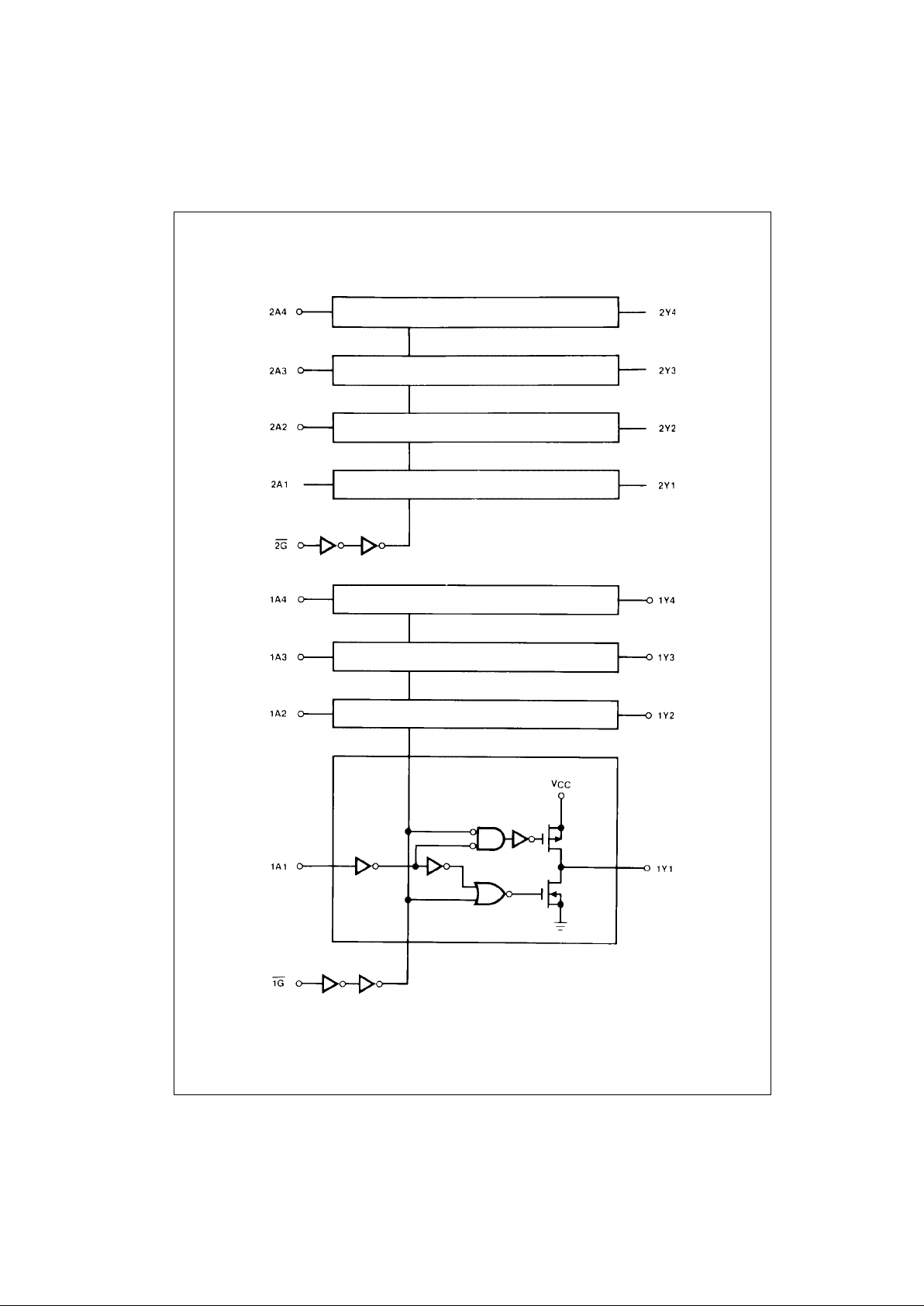
Logic Diagram
Page 3
3 www.fairchildsemi.com
MM74HC244
Absolute Maximum Ratings(Note 1)
(Note 2)
Recommended Operating
Conditions
Note 1: Absolute Maximum Ratings are those values beyond which dam-
age to the device may occur.
Note 2: Unless otherwise specified all voltages are referenced to ground.
Note 3: Power Dissipation te mperature d erating — pl astic “N” package: −
12 mW/°C from 65°C to 85°C.
DC Electrical Characteristics (Note 4)
Note 4: For a power supply of 5V ± 10% the worst case output voltages (VOH, and VOL) occur for HC at 4.5V. Thus the 4.5V values should be used when
designing with this supply. Worst case V
IH
and VIL occur at VCC = 5.5V and 4.5 V respectively. (The VIH value at 5.5V is 3.85V.) The worst case leakage cur-
rent (I
IN
, ICC, and IOZ) occur for CMOS at the higher voltage and so th e 6. 0V values should be use d.
Supply Voltage (VCC) −0.5 to +7.0V
DC Input Voltage (V
IN
) −1.5 to V
CC
+1.5V
DC Output Voltage (V
OUT
) −0.5 to V
CC
+0.5V
Clamp Diode Current (I
IK
, IOK) ± 20 mA
DC Output Current, per pin (I
OUT
) ± 35 mA
DC V
CC
or GND Current, per pin (ICC) ± 70 mA
Storage Temperature Range (T
STG
) −65°C to +150°C
Power Dissipation (P
D
)
(Note 3) 600 mW
S.O. Package only 500 mW
Lead Temperature (T
L
)
(Solderi ng 10 seconds) 260
°C
Min Max Units
Supply Voltage (V
CC
)26V
DC Input or Output Voltage
(V
IN
, V
OUT
)0V
CC
V
Operating Temperature Range (T
A
) −40 +85 °C
Input Rise or Fall Times
(t
r
, tf) V
CC
= 2.0V 1000 ns
V
CC
= 4.5V 500 ns
V
CC
= 6.0V 400 ns
Symbol Parameter Conditions
V
CC
TA = 25°CTA = −40 to 85°CTA = −55 to 125°C
Units
Typ Guaranteed Limits
V
IH
Minimum HIGH Level 2.0V 1.5 1.5 1.5 V
Input Voltage 4.5V 3.15 3.15 3.15 V
6.0V 4.2 4.2 4.2 V
V
IL
Maximum LOW Level 2.0V 0.5 0.5 0.5 V
Input Voltage 4.5V 1.35 1.35 1.35 V
6.0V 1.8 1.8 1.8 V
V
OH
Minimum HIGH Level V
IN
= VIH or V
IL
Output Voltage |I
OUT
| ≤ 20 µA 2.0V 2.0 1.9 1.9 1.9 V
4.5V 4.5 4.4 4.4 4.4 V
6.0V 6.0 5.9 5.9 5.9 V
V
IN
= VIH or V
IL
V
|I
OUT
| ≤ 6.0 mA 4.5V 4.2 3.98 3.84 3.7 V
|I
OUT
| ≤ 7.8 mA 6.0V 5.7 5.4 5.34 5.2 V
V
OL
Maximum LOW Level V
IN
= VIH or V
IL
Output Voltage |I
OUT
| ≤ 20 µA 2.0V 0 0.1 0.1 0.1 V
4.5V 0 0.1 0.1 0.1 V
6.0V 0 0.1 0.1 0.1 V
V
IN
= VIH or V
IL
|I
OUT
| ≤ 6.0 mA 4.5V 0.2 0.26 0.33 0.4 V
|I
OUT
| ≤ 7.8 mA 6.0V 0.2 0.26 0.33 0.4 V
I
IN
Maximum Input V
IN
= VCC or GND 6.0V ± 0.1 ± 1.0 ±1.0 µA
Current
I
OZ
Maximum 3-STATE V
IN
= VIH, or V
IL
6.0V ± 0.5 ± 5 ±10 µA
Output Leakage V
OUT
= VCC or GND
Current G = V
IH
I
CC
Maximum Quiescent V
IN
= VCC or GND 6.0V 8.0 80 160 µA
Supply Current I
OUT
= 0 µA
Page 4
www.fairchildsemi.com 4
MM74HC244
AC Electrical Characteristics
V
CC
= 5V, TA = 25°C, tr = t
f
= 6 ns
AC Electrical Characteristics
V
CC
= 2.0V-6.0V, CL = 50 pF, tr = t
f
= 6 ns (unless otherwise specified)
Note 5: CPD determines the no lo ad dynamic power cons um ption, PD = CPD V
CC
2
f + ICC VCC, and the no load dynam ic c urrent consumption,
I
S
= CPD VCCf + ICC.
Symbol Parameter Conditions Typ
Guaranteed
Units
Limit
t
PHL
, t
PLH
Maximum Propagation CL = 45 pF 14 20 ns
Delay
t
PZH
, t
PZL
Maximum Enable Delay RL = 1 kΩ 17 28 ns
to Active Output C
L
= 45 pF
t
PHZ
, t
PLZ
Maximum Disable Delay RL = 1 kΩ 15 25 ns
from Active Output CL = 5 pF
Symbol Parameter Conditions
V
CC
TA = 25°CTA = −40 to 85°C TA = −55 to 125°C
Units
Typ Guaranteed Limits
t
PHL
, t
PLH
Maximum Propagation CL = 50 pF 2.0V 58 115 145 171 ns
Delay CL = 150 pF 2.0V 83 165 208 246 ns
C
L
= 50 pF 4.5V 14 23 29 34 ns
C
L
= 150 pF 4.5V 17 33 42 49 ns
CL = 50 pF 6.0V 10 20 25 29 ns
C
L
= 150 pF 6.0V 14 28 35 42 ns
t
PZH
, t
PZL
Maximum Output Enable RL = 1 kΩ
Time CL = 50 pF 2.0V 75 150 189 224 ns
C
L
= 150 pF 2.0V 100 200 252 298 ns
C
L
= 50 pF 4.5V 15 30 38 45 ns
CL = 150 pF 4.5V 30 40 50 60 ns
C
L
= 50 pF 6.0V 13 26 32 38 ns
C
L
= 150 pF 6.0V 17 34 43 51 ns
t
PHZ
, t
PLZ
Maximum Output Disable RL = 1 kΩ 2.0V 75 150 189 224 ns
Time C
L
= 50 pF 4.5V 15 30 38 45 ns
6.0V 13 26 32 38 ns
t
TLH
, t
THL
Maximum Output 2.0V 60 75 90 ns
Rise and Fall Time 4.5V 12 15 18 ns
6.0V 10 13 15 ns
C
PD
Power Dissipation (per buffer)
Capacitance (Note 5) G
= V
IH
12 pF
G
= V
IL
50 pF
C
IN
Maximum Input 5 10 10 10 pF
Capacitance
C
OUT
Maximum Output 10 20 20 20 pF
Capacitance
Page 5
5 www.fairchildsemi.com
MM74HC244
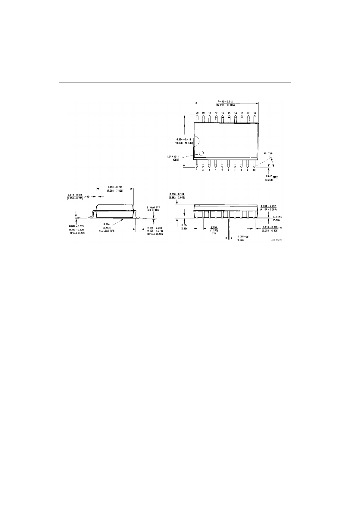
Physical Dimensions inches (millimeters) unless otherwise noted
20-Lead Small Outline Integrated Circuit (SOIC), JEDEC MS-013, 0.300 Wide
Package Number M20B
Page 6
www.fairchildsemi.com 6
MM74HC244
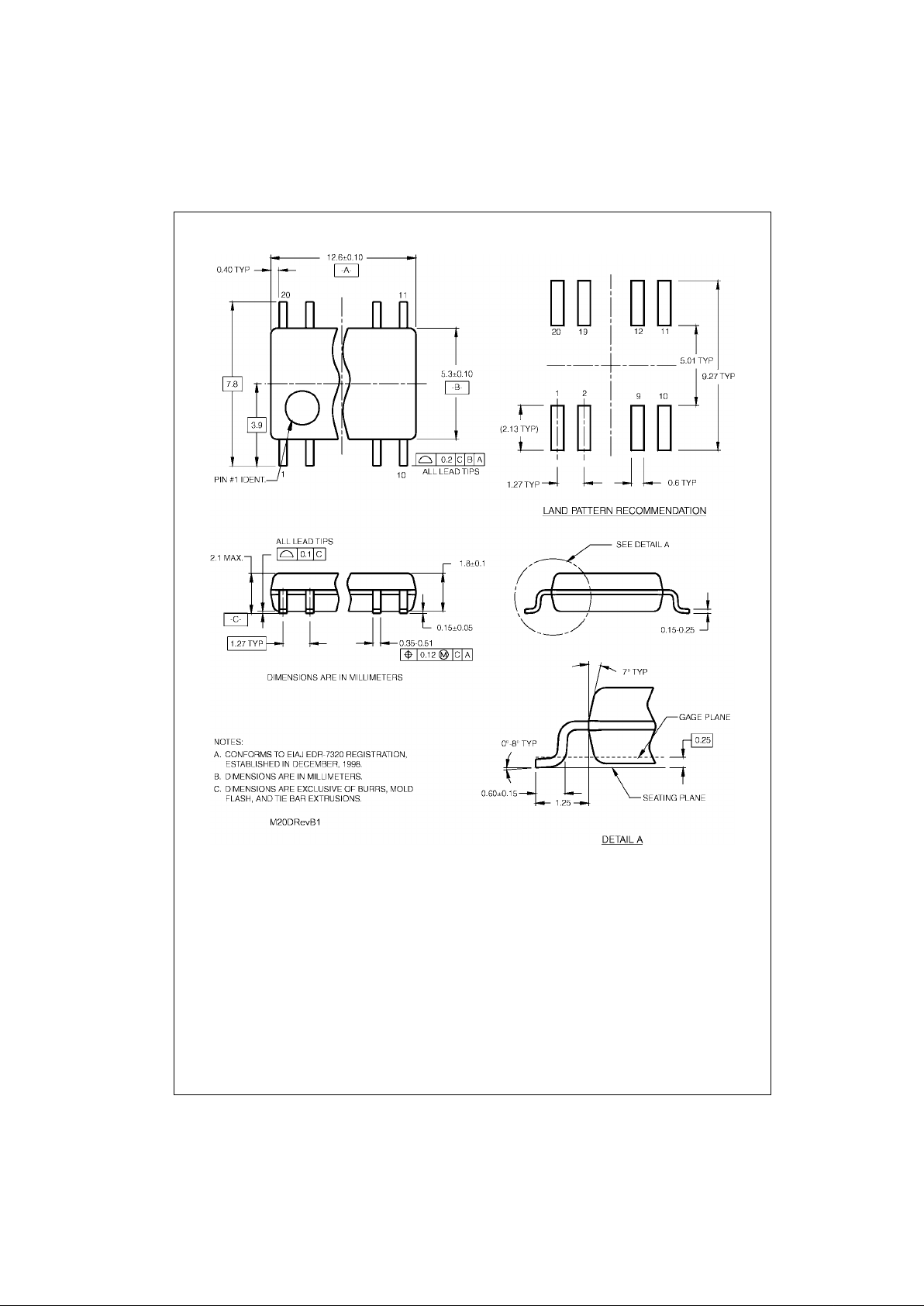
Physical Dimensions inches (millimeters) unless otherwise noted (Continued)
20-Lead Small Outline Package (SOP), EIAJ TYPE II, 5.3mm Wide
Package Number M20D
Page 7
7 www.fairchildsemi.com
MM74HC244
Physical Dimensions inches (millimeters) unless otherwise noted (Continued)
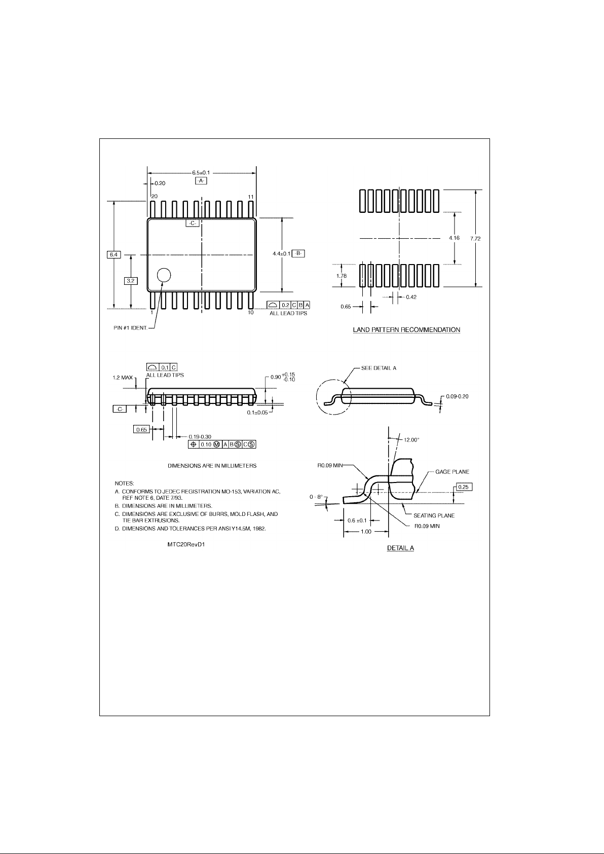
20-Lead Thin Shrink Sm all Ou tline Pa ck age (TS SO P), JE DE C MO-153, 4.4mm Wide
Package Number MTC20
Page 8

www.fairchildsemi.com 8
MM74HC244 Octal 3-STATE Buffer
Physical Dimensions inches (millimeters) unless otherwise noted (Continued)
20-Lead Plastic Dual-In-Line Package (PDIP), JEDEC MS-001, 0.300” Wide
Package Number N20A
Fairchild does not assume any responsibility for use of any circuitr y described, no circuit patent licenses are implied and
Fairchild reserves the right at any time without notice to change said circuitry and specifications.
LIFE SUPPORT POLICY
FAIRCHILD’S PRODUCTS ARE NOT AUTHORIZED FOR USE AS CRITICAL COMPONENTS IN LIFE SUPPORT
DEVICES OR SYSTEMS WITHOUT THE EXPRESS WRITTEN APPROVAL OF THE PRESIDENT OF FAIRCHILD
SEMICONDUCTOR CORPORATION. As used herein:
1. Life support devices or systems are devices or syste ms
which, (a) are intended for surgical implant into the
body, or (b) support or sustain life, and (c) whose failure
to perform when properly used in accordance with
instructions for use provided in the labeling, can be reasonably expected to result in a significant inju ry to the
user.
2. A critical component in any compon ent of a lif e supp ort
device or system whose failure t o perform can be reasonably expected to ca use the failure of the life supp ort
device or system, or to affect its safety or effectiveness.
www.fairchildsemi.com
 Loading...