

Datasheet MM74HC221AN, MM74HC221AM, MM74HC221ACW, MM74HC221CW, MM74HC221ASJ Datasheet (Fairchild Semiconductor)
...Page 1
September 1983
Revised February 1999
MM74HC221A Dual Non-Retriggerable Monostable Multivibrator
© 1999 Fairchild Semiconductor Corporation DS005325.prf www.fairchildsemi.com
MM74HC221A
Dual Non-Retriggerable Monostable Multivibrator
General Description
The MM74HC221A high spe ed monostable multivibrato rs
(one shots) utilize advanced silicon-gate CMOS technology. They feature speeds comparab le to low p ower S chottky TTL circuitry while retaining the low p ower and high
noise immunity characteristic of CMOS circuits.
Each multivibrator fea tures b oth a n egative , A, a nd a po sitive, B, transition trigg ered input, either of which can be
used as an inhibit input. Also includ ed is a clear input that
when taken low resets t he one shot. The MM74HC221A
can be triggered on the positive transition of the clear while
A is held LOW and B is held HIGH.
The MM74HC221A is a non-retriggerable, and therefore
cannot be retriggered until the output pulse times out.
Pulse width stability over a wide range of temperature and
supply is achieved using linear CMOS techniques. The output pulse equation is sim ply: PW = (R
EXT
) (C
EXT
); where
PW
is in seconds, R is in ohms, and C is in farads. All inputs
are protected from damage due to static discharge by
diodes to V
CC
and ground.
Features
■ Typical propagation delay: 40 ns
■ Wide power supply range: 2V–6V
■ Low quiescent current: 80 µA maximum (74HC Series)
■ Low input current: 1 µA maximum
■ Fanout of 10 LS-TTL loads
■ Simple pulse width formula T = RC
■ Wide pulse range: 400 ns to ∞ (typ)
■ Part to part variation: ±5% (typ)
■ Schmitt Trigger A & B inputs enab le infinite signa l input
rise or fall times
Ordering Code:
Devices also availab le in Tape and Reel. Specify by appending th e s uffix let t er “X” to the ordering cod e.
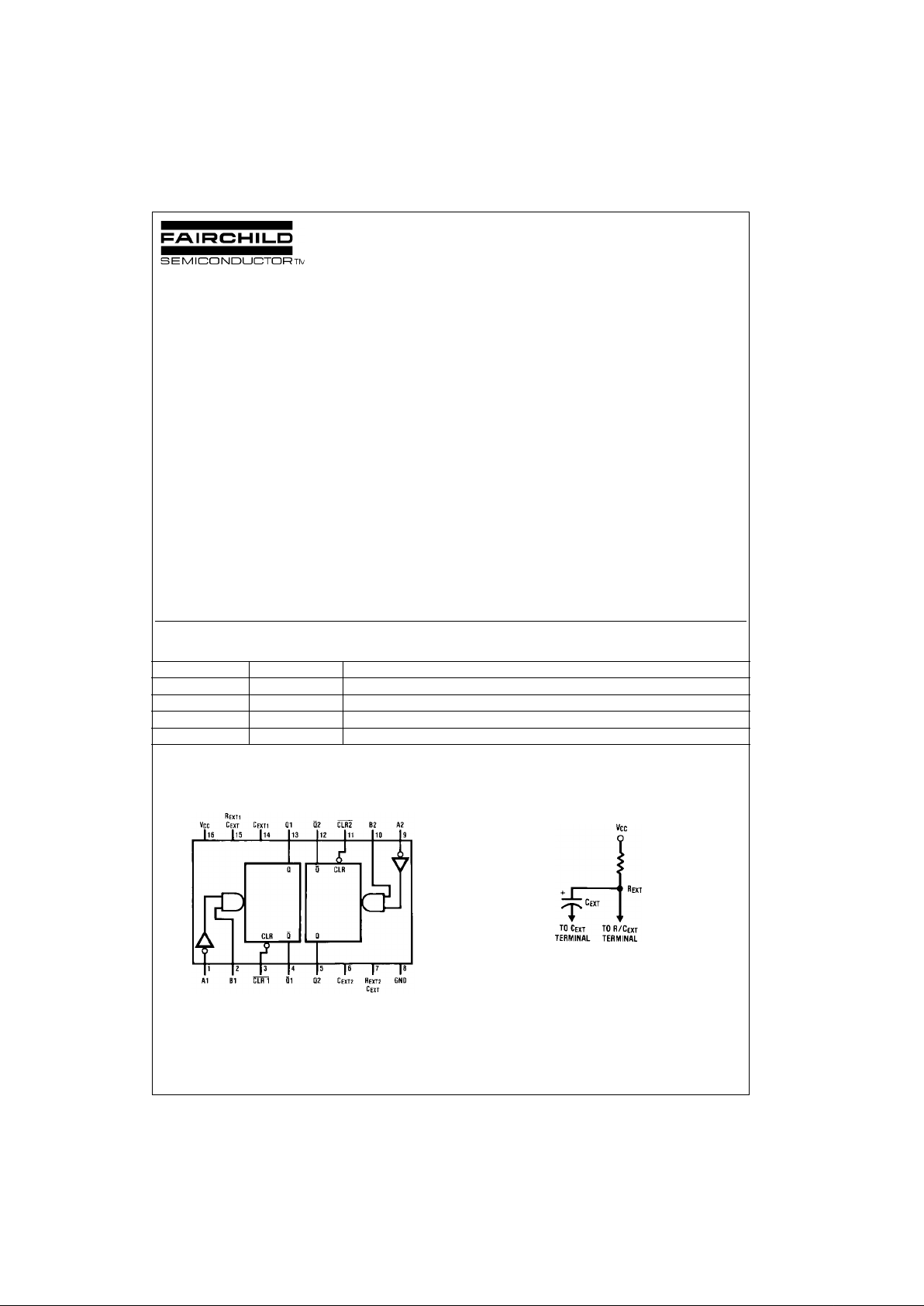
Connection Diagrams
Pin Assignments f or DIP, SOIC, SOP and TSSOP
Top View
Timing Component
Note: Pin 6 and Pin 14 mus t be hard-wired to GND .
Order Number Package Number Package Description
MM74HC221AM M16A 16-Lead Small Outline Integrated Circuit (SOIC), JEDEC MS-012, 0.150” Narrow
MM74HC221ASJ M16D 16-Lead Small Outline Package (SOP), EIAJ TYPE II, 5.3mm Wide
MM74HC221AMTC MTC16 16-Lead Thin Shrink Small Outline Package (TSSOP), JEDEC MO-153, 4.4mm Wide
MM74HC221A N N16E 16-Lead Plas tic Dual-I n-Line Package (PDIP), MS-001, 0.300” Wide
Page 2
www.fairchildsemi.com 2
MM74HC221A
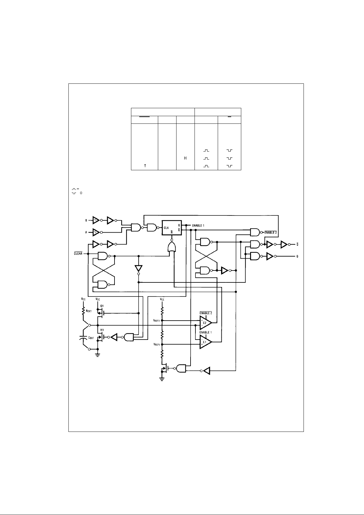
Truth Table
H = HIGH Level
L = LOW Level
↑= Transition from LOW-to-HIGH
↓= Transition from HIGH-to-L OW
= One HIGH Level Pulse
= One LOW Level Pulse
X = Irrelevant
Logic Diagram
Inputs Outputs
Clear
AB Q Q
LXXLH
XHXLH
XXLLH
HL↑
H ↓ H
↑ LH
Page 3
3 www.fairchildsemi.com
MM74HC221A
Absolute Maximum Ratings(Note 1)
(Note 2)
Recommended Operating
Conditions
Note 1: Maximum Ratings are those values beyond which damage to the
device may occur.
Note 2: Unless otherwise specified all voltages are referenced to ground.
Note 3: Power Dissipation te mperature d erating — pl astic “N” pa ckage: −
12 mW/°C from 65°C to 85°C.
DC Electrical Characteristics (Note 4)
Note 4: For a powe r supply o f 5V ±10% the worst-case output voltages (VOH, and VOL) occur for HC at 4.5V. Thus the 4. 5V valu es shou ld be u sed when
designing with this s upply. Worst-case V
IH
and VIL occur at V
CC
= 5.5V and 4.5V res pectively. (The VIH value at 5.5V is 3.85V.) The worst-case leakage cur-
rent (I
IN
, ICC, and IOZ) occur for CMOS at the higher voltage and so th e 6. 0V values should be used.
Supply Voltage (VCC) −0.5V to +7.0V
DC Input Voltage (V
IN
) −1.5V to VCC+1.5V
DC Output Voltage (V
OUT
) −0.5V to VCC+0.5V
Clamp Diode Current (I
IK
, IOK) ±20 mA
DC Output Current, per pin (I
OUT
) ±25 mA
DC V
CC
or GND Current, per pin (ICC) ±50 mA
Storage Temperature Range (T
STG
) −65°C to +150°C
Power Dissipation (P
D
)
(Note 3) 600 mW
S.O. Package only 500 mW
Lead Temperature (T
L
)
(Soldering 10 seconds) 260°C
Min Max Units
Supply Voltage (V
CC
)26V
DC Input or Output Voltage
(V
IN
, V
OUT
)0V
CC
V
Operating Temperature Range (T
A
) −40 +85 °C
Maximum Inpu t Rise and Fall
Time (Clear Input)
V
CC
= 2.0V 1000 ns
V
CC
= 4.5V 500 ns
V
CC
= 6.0V 400 ns
Symbol Parameter Conditions
V
CC
TA = 25°CTA = −40 to 85°CTA = −55 to 125°C
Units
Typ Guaranteed Limits
V
IH
Minimum HIGH Level 2.0V 1.5 1.5 1.5 V
Input Voltage 4.5V 3.15 3.15 3.15 V
6.0V 4.2 4.2 4.2 V
V
IL
Maximum LOW Level 2.0V 0.3 0.3 0.3 V
Input Voltage 4.5V 0.9 0.9 0.9 V
6.0V 1.2 1.2 1.2 V
V
OH
Minimum HIGH Level V
IN
= VIH or V
IL
Output Voltage |I
OUT
| ≤ 20 µA 2.0V 2.0 1.9 1.9 1.9 V
4.5V 4.5 4.4 4.4 4.4 V
6.0V 6.0 5.9 5.9 5.9 V
V
IN
= VIH or V
IL
|I
OUT
| ≤ 4.0 mA 4.5V 4.2 3.98 3.84 3.7 V
|I
OUT
| ≤ 5.2 mA 6.0V 5.7 5.48 5.34 5.2 V
V
OL
Maximum LOW Level V
IN
= VIH or V
IL
Output Voltage |I
OUT
| ≤ 20 µA 2.0V 0 0.1 0.1 0.1 V
4.5V 0 0.1 0.1 0.1 V
6.0V 0 0.1 0.1 0.1 V
V
IN
= VIH or V
IL
|I
OUT
| ≤ 4.0 mA 4.5V 0.2 0.26 0.33 0.4 V
|I
OUT
| ≤ 5.2 mA 6.0V 0.2 0.26 0.33 0.4 V
I
IN
Maximum Input Current V
IN
= VCC or GND 6.0V ±0.5 ±5.0 ±5.0 µA
(Pins 7, 15)
I
IN
Maximum Input Current V
IN
= VCC or GND 6.0V ±0.1 ±1.0 ±1.0 µA
(all other pins)
I
CC
Maximum Quiescent Supply V
IN
= VCC or GND 6.0V 8.0 80 160 µA
Current (standby) I
OUT
= 0 µA
I
CC
Maximum Active Supply V
IN
= VCC or GND 2.0V 36 80 110 130 µA
Current (per monostable) R/C
EXT
= 0.5V
CC
4.5V 0.33 1.0 1.3 1.6 mA
6.0V 0.7 2.0 2.6 3.2 mA
Page 4

www.fairchildsemi.com 4
MM74HC221A
AC Electrical Characteristics
V
CC
= 5V, TA = 25°C, CL = 15 pF, tr = t
f
= 6 ns
AC Electrical Characteristics
C
L
= 50 pF, tr = t
f
= 6 ns (unless otherwise specified)
Note 5: CPD determines the no lo ad dynamic power con s um ption, PD = CPD V
CC
2
f + ICC VCC, and the no load dynamic current consum pt ion,
I
S
= CPD VCCf + ICC.
Symbol Parameter Conditions Typ
Guaranteed
Units
Limit
t
PLH
Maximum Trigger Propagation 22 36 ns
Delay A, B or Clear to Q
t
PHL
Maximum Trigger Propagation 25 42 ns
Delay A, B or Clear to Q
t
PHL
Maximum Propagation Delay Clear to Q 20 31 ns
t
PLH
Maximum Propagation Delay Clear to Q
22 33 ns
t
W
Minimum Pulse Width A, B or C lear 14 26 ns
t
REM
Minimum Clear Removal Time 0ns
t
WQ(MIN)
Minimum Output Pulse Width C
EXT
= 28 pF 400 ns
R
EXT
= 2 kΩ
t
WQ
Output Pulse Width C
EXT
= 1000 pF 10 µs
R
EXT
= 10 kΩ
Symbol Parameter Conditions
V
CC
TA = 25°CTA = −40 to 85°CTA = −55 to 125°C
Units
Typ Guaranteed Limits
t
PLH
Maximum Trigger Propagation 2.0V 77 169 194 210 ns
Delay A, B or Clear to Q 4.5V 26 42 51 57 ns
6.0V 21 32 39 44 ns
t
PHL
Maximum Trigger Propagation 2.0V 88 197 229 250 ns
Delay A, B or Clear to Q
4.5V 29 48 60 67 ns
6.0V 24 38 46 51 ns
t
PHL
Maximum Propagation 2.0V 54 114 132 143 ns
Delay Clear to Q 4.5V 23 34 41 45 ns
6.0V 19 28 33 36 ns
t
PLH
Maximum Propagation 2.0V 56 116 135 147 ns
Delay Clear to Q
4.5V 25 36 42 46 ns
6.0V 20 29 34 37 ns
t
W
Minimum Pulse Width 2.0V 57 123 144 157 ns
A, B, Clear 4.5V 17 30 37 42 ns
6.0V 12 21 27 30 ns
t
REM
Minimum Clear 2.0V 0 0 0 ns
Removal Time 4.5V 0 0 0 ns
6.0V 0 0 0 ns
t
TLH
, t
THL
Maximum Output 2.0V 30 75 95 110 ns
Rise and Fall Time 4.5V 8 15 19 22 ns
6.0V 7 13 16 19 ns
t
WQ(MIN)
Minimum Output C
EXT
= 28 pF 2.0V 1.5 µs
Pulse Width R
EXT
= 2 kΩ 4.5V 450 ns
R
EXT
= 6 kΩ (V
CC
= 2V) 6.0V 380 ns
t
WQ
Output Pulse Width C
EXT
= 0.1 µF Min 5.0V 1 0.9 0.86 0.85 ms
R
EXT
= 10 kΩ
Max 5.0V 1 1.1 1.14 1.15 ms
C
PD
Power Dissipation 87 pF
Capacitance (Note 5)
C
IN
Maximum Input 12 20 20 20 pF
Capacitance (Pins 7 & 15)
C
IN
Maximum Input 6 10 10 10 pF
Capacitance (other inputs)
Page 5

5 www.fairchildsemi.com
MM74HC221A
Theory of Operation
FIGURE 1.
TRIGGER OPERATION
As shown in
Figure 1
and the logic diagram before an input
trigger occurs, the monostable is in the quiescent state with
the Q output LOW, and the timing capacitor C
EXT
com-
pletely charged to V
CC
. When the trigger input A goes from
V
CC
to GND (while inputs B and clear are held to VCC) a
valid trigger is recognized, which turns on comparator C1
and N-channel transisto r N 11. At the same time th e outp ut
latch is set. With transistor N1 on, the ca pacitor C
EXT
rap-
idly discharges toward GND until V
REF1
is reached. At this
point the output o f c ompar ator C 1 c hanges state an d tra nsistor N1 turns off. Comparator C1 then turns off while at
the same time compar ato r C2 tu rns on . W ith tr ans is tor N1
off, the capacitor C
EXT
begins to charge through the timing
resistor, R
EXT
, toward VCC. When the voltage across C
EXT
equals V
REF2
, comparator C2 change s state causing the
output latch to reset (Q goe s LOW) wh ile at the sa me time
disabling comparator C2. T his ends the timing cycle with
the monostable in the quiescent state, waiting for the next
trigger.
A valid trigger is also recognized when trigger input B goes
from GND to V
CC
(while input A is at GND and input clear
is at V
CC
2). The MM74HC22 1 can al so be tr iggered wh en
clear goes from GN D to V
CC
(while A is at Gnd and B is at
V
CC
6).
It should be note d that in the quie scent state C
EXT
is fully
charged to V
CC
causing the current through resistor R
EXT
to be zero. Both compara tors are “off” with th e total d evice
current due only to reverse junction leakages. An added
feature of the MM74HC221 is that the output latch is set via
the input trigger without regar d to the capacitor voltage.
Thus, propagation delay from trigger to Q is independent of
the value of C
EXT
, R
EXT
, or the duty cycle of the input
waveform.
The MM74HC221 is non-retriggerable and will ignore input
transitions on A and B until it has timed out 3 and 4.
RESET OPERATION
These one shots may be reset during the generation of the
output pulse. In the reset mode of operation, an input pulse
on clear sets the reset latch and causes the capacitor to be
fast charged to V
CC
by turning on tr ansistor Q1 5. When
the voltage on the capacitor reaches V
REF2
, the reset latch
will clear and then be ready to accep t another p ulse. If the
clear input is held LOW, any trigger inputs that occur will be
inhibited and the Q and Q
outputs of the output la tch will
not change. Since the Q output i s reset when an input low
level is detected on the Clear input, th e out put pulse T can
be made significantly shorter than the minimum pulse width
specification.
Page 6

www.fairchildsemi.com 6
MM74HC221A
Typical Output Pulse Width
vs. Timing Components
Typical Distribution of Output
Pulse Width, Part to Part
Typical 1ms Pulse Width
Variation vs. Supply
Minimum R
EXT
vs.
Supply Voltage
Typical 1 ms Pulse Width
Variation vs. Temperature
Note: R and C are not subjected to temperature. The C is polypropylene.
Page 7

7 www.fairchildsemi.com
MM74HC221A
Physical Dimensions inches (millimeters) unless otherwise noted
16-Lead Small Outline Integrated Circuit (SOIC), JEDEC MS-012, 0.150” Narrow
Package Number M16A
16-Lead Small Outline Package (SOP), EIAJ TYPE II, 5.3mm Wide
Package Number M16D
Page 8

www.fairchildsemi.com 8
MM74HC221A
Physical Dimensions inches (millimeters) unless otherwise noted (Continued)
16-Lead Thin Shrink Small Outline Package (TSSOP), JEDEC MO-153, 4.4mm Wide
Package Number MTC16
Page 9

Fairchild does not assume any responsibility for use of any circuitry described, no circuit patent licenses are implied and Fairchild reserves the right at any time without notice to change said circuitry and specifications.
MM74HC221A Dual Non-Retriggerable Monostable Multivibrator
LIFE SUPPORT POLICY
FAIRCHILD’S PRODUCTS ARE NOT AUTHORIZED FOR USE AS CRITICAL COMPONENTS IN LIFE SUPPORT
DEVICES OR SYSTEMS WITHOUT THE EXPRESS WRITTEN APPROVAL OF THE PRESIDENT OF FAIRCHILD
SEMICONDUCTOR CORPORATION. As used herein:
1. Life support de vices o r syst ems are devices or systems
which, (a) are intended for surgical implant into the
body, or (b) support or sustain life, and (c) whose failure
to perform when properly used in accordance with
instructions for use provided i n the labe li ng, can be re asonably expected to result in a significant injury to the
user.
2. A critica l compo nent i n any compo nent o f a life s uppor t
device or system whose failu re to perform can b e reasonably expected to c ause th e fa i lure of the li fe s upp or t
device or system, or to affect its safety or effectiveness.
www.fairchildsemi.com
Physical Dimensions inches (millimeters) unless otherwise noted (Continued)
16-Lead Plastic Dual-In-Line Package (PDIP), JEDEC MS-001, 0.300” Wide
Package Number N16E
 Loading...