

Datasheet MM74HC174MX, MM74HC174N, MM74HC174SJ, MM74HC174MTC, MM74HC174M Datasheet (Fairchild Semiconductor)
...Page 1
September 1983
Revised February 1999
MM74HC174 Hex D-Type Flip-Flops with Clear
© 1999 Fairchild Semiconductor Corporation DS005318.prf www.fairchildsemi.com
MM74HC174
Hex D-Type Flip-Flops with Clear
General Description
The MM74HC174 edge triggered flip-flops utilize advanced
silicon-gate CMOS technology to implement D-type flipflops. They possess high no ise immunity, low power, and
speeds comparable to low power Schottky TTL circuits.
This device contains 6 master-slave flip- flops with a common clock and common clear. Data on the D in put having
the specified setup and hold times is transferred to th e Q
output on the LOW-to-HIGH transition of the CLOCK input.
The CLEAR input when LOW, sets all outputs to a low
state.
Each output can drive 10 low p ower Schottk y TTL eq uivalent loads. The MM74HC174 is functionally as well as pin
compatible to the 74L S174. All inputs are protected fr om
damage due to static discharge by diodes to V
CC
and
ground.
Features
■ Typical propagation delay: 16 ns
■ Wide operating voltage range: 2–6V
■ Low input current: 1 µA maximum
■ Low quiescent current: 80 µA (74HC Series)
■ Output drive: 10 LSTTL loads
Ordering Code:
Devices also availab le in Tape and Reel. Specify by appending th e s uffix let t er “X” to the ordering cod e.
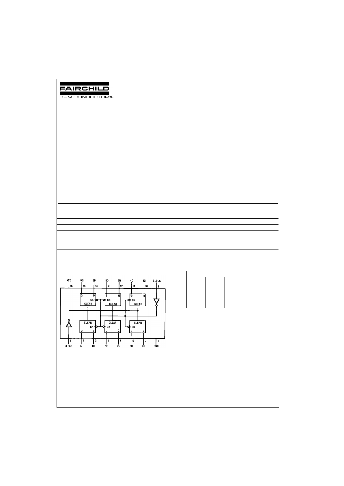
Connection Diagram
Pin Assignments f or DIP, SOIC, SOP and TSSOP
Truth Table
(Each Flip-Flop)
H = HIGH Level (steady state)
L = LOW Level (steady state)
X = Don't Care
↑ = Transition from LOW-to-HIGH level
Q
0
= The level of Q before the indic ated steady stat e input conditions were
established.
Order Number Package Number Package Description
MM74HC174M M16A 16-Lead Small Outline Integrated Circuit (SOIC), JEDEC MS-012, 0.150” Narrow
MM74HC174SJ M16D 16-Lead Small Outline Package (SOP), EIAJ TYPE II, 5.3mm Wide
MM74HC174MTC MTC16 16-Lead Thin Shrink Small Outline Package (TSSOP), JEDEC MO-153, 4.4mm Wide
MM74HC174N N16E 16-Lead Plastic Dual-In-Line Package (PDIP), JEDEC MS-001, 0.300” Wide
Inputs Outputs
Clear Clock D Q
LXXL
H ↑ HH
H ↑ LL
HLXQ
0
Page 2
www.fairchildsemi.com 2
MM74HC174
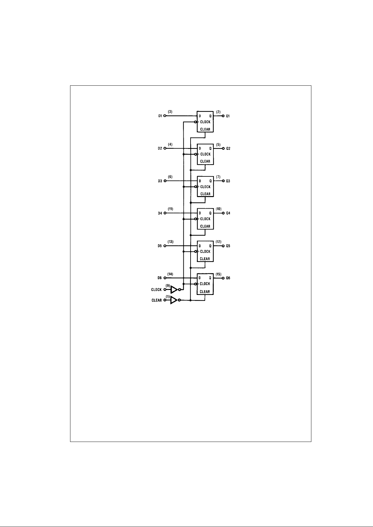
Logic Diagram
Page 3
3 www.fairchildsemi.com
MM74HC174
Absolute Maximum Ratings(Note 1)
(Note 2)
Recommended Operating
Conditions
Note 1: Absolute Maximum Ra tings are those valu es beyond w hich dam-
age to the device may occur.
Note 2: Unless otherwise specified all voltages are referenced to ground.
Note 3: Power Dissipation te mperature d erating — pl astic “N” pa ckage: −
12 mW/°C from 65°C to 85°C.
DC Electrical Characteristics (Note 4)
Note 4: For a powe r supply o f 5V ±10% the worst case output voltages (VOH, and VOL) occur for HC at 4.5V. Thus the 4. 5V valu es shou ld be u sed when
designing with this supply. Worst case V
IH
and VIL occur at V
CC
= 5.5V and 4.5V respectively. (The VIH value at 5.5V is 3 .8 5V.) The worst c as e leakage cur-
rent (I
IN
, ICC, and IOZ) occur for CMOS at the higher voltage and so th e 6. 0V values should be used.
Supply Voltage (VCC) −0.5 to +7.0V
DC Input Voltage (V
IN
) −1.5 to V
CC
+1.5V
DC Output Voltage (V
OUT
) −0.5 to V
CC
+0.5V
Clamp Diode Current (I
IK
, IOK) ±20 mA
DC Output Current, per pin (I
OUT
) ±25 mA
DC V
CC
or GND Current, per pin (ICC) ±50 mA
Storage Temperature Range (T
STG
) −65°C to +150°C
Power Dissipation (P
D
)
(Note 3) 600 mW
S.O. Package only 500 mW
Lead Temperature (T
L
)
(Solderi ng 10 seconds) 260°C
Min Max Units
Supply Voltage (V
CC
)26V
DC Input or Output Voltage
(V
IN
, V
OUT
)0V
CC
V
Operating Temperature Range (T
A
) −40 +85 °C
Input Rise or Fall Times
(t
r
, tf) V
CC
= 2.0V 1000 ns
V
CC
= 4.5V 500 ns
V
CC
= 6.0V 400 ns
Symbol Parameter Conditions
V
CC
TA = 25°CTA = −40 to 85°CTA = −55 to 125°C
Units
Typ Guaranteed Limits
V
IH
Minimum HIGH Level 2.0V 1.5 1.5 1.5 V
Input Voltage 4.5V 3.15 3.15 3.15 V
6.0V 4.2 4.2 4.2 V
V
IL
Maximum LOW Level 2.0V 0.5 0.5 0.5 V
Input Voltage 4.5V 1.35 1.35 1.35 V
6.0V 1.8 1.8 1.8 V
V
OH
Minimum HIGH Level V
IN
= VIH or V
IL
Output Voltage |I
OUT
| ≤ 20 µA 2.0V 2.0 1.9 1.9 1.9 V
4.5V 4.5 4.4 4.4 4.4 V
6.0V 6.0 5.9 5.9 5.9 V
V
IN
= VIH or V
IL
|I
OUT
| ≤ 4.0 mA 4.5V 4.2 3.98 3.84 3.7 V
|I
OUT
| ≤ 5.2 mA 6.0V 5.7 5.48 5.34 5.2 V
V
OL
Maximum LOW Level V
IN
= VIH or V
IL
Output Voltage |I
OUT
| ≤ 20 µA 2.0V 0 0.1 0.1 0.1 V
4.5V 0 0.1 0.1 0.1 V
6.0V 0 0.1 0.1 0.1 V
V
IN
= VIH or V
IL
|I
OUT
| ≤ 4.0 mA 4.5V 0.2 0.26 0.33 0.4 V
|I
OUT
| ≤ 5.2 mA 6.0V 0.2 0.26 0.33 0.4 V
I
IN
Maximum Input V
IN
= VCC or GND 6.0V ±0.1 ±1.0 ±1.0 µA
Current
I
CC
Maximum Quiescent V
IN
= VCC or GND 6.0V 8.0 80 160 µA
Supply Current I
OUT
= 0 µA
Page 4

www.fairchildsemi.com 4
MM74HC174
AC Electrical Characteristics
V
CC
= 5V, TA = 25°C, CL = 15pF, tr = tf = 6 ns
AC Electrical Characteristics
C
L
= 50 pF, tr = t
f
= 6 ns (unless otherwise specified)
Note 5: CPD determines the no lo ad dynamic power con su m pt ion, PD = CPD V
CC
2
f + ICC VCC, and the no load dynam ic c urrent consumption ,
I
S
= CPDVCCf + ICC.
Symbol Parameter Conditions Typ
Guaranteed
Units
Limit
f
MAX
Maximum Operating 50 30 MHz
Frequency
t
PHL
, t
PLH
Maximum Propagation 16 30 ns
Delay, Clock or Clear to Output
t
REM
Minimum Removal Time, −25ns
Clear to Clock
t
S
Minimum Setup Time 10 20 ns
Data to Clock
t
H
Minimum Hold Time 0 5 ns
Clock to Data
t
W
Minimum Pulse Width 10 16 ns
Clock or Clear
Symbol Parameter Conditions
V
CC
TA = 25°CTA = −40 to 85°CTA = −55 to 125°C
Units
Typ Guaranteed Limits
f
MAX
Maximum Operating 2.0V 5 4 3 MHz
Frequency 4.5V 27 21 18 MHz
6.0V 31 24 20 MHz
t
PHL
, t
PLH
Maximum Propagation 2.0V 55 165 206 248 ns
Delay Clock or Clear to Output 4.5V 18 33 41 49 ns
6.0V 16 28 35 42 ns
t
REM
Minimum Removal Time 2.0V 1 5 5 5 ns
Clear to Clock 4.5V 1 5 5 5 ns
6.0V 1 5 5 5 ns
t
S
Minimum Setup Time 2.0V 42 100 125 150 ns
Data to Clock 4.5V 12 20 25 30 ns
6.0V 10 17 21 25 ns
t
H
Minimum Hold Time 2.0V 1 5 5 5 ns
Clock to Data 4.5V 1 5 5 5 ns
6.0V 1 5 5 5 ns
t
W
Minimum Pulse Width 2.0V 35 80 106 120 ns
Clock or Clear 4.5V 10 16 20 24 ns
6.0V 8 14 18 20 ns
t
TLH
, t
THL
Maximum Output Rise 2.0V 30 75 95 110 ns
and Fall Time 4.5V 8 15 19 22 ns
6.0V 7 13 16 19 ns
tr, t
f
Maximum Input Rise and 2.0V 1000 1000 1000 ns
Fall Time 4.5V 500 500 500 ns
6.0V 400 400 400 ns
C
PD
Power Dissipation (per package) 136 pF
Capacitance (Note 5)
C
IN
Maximum Input 5 10 10 10 pF
Capacitance
Page 5

5 www.fairchildsemi.com
MM74HC174
Physical Dimensions inches (millimeters) unless otherwise noted
16-Lead Small Outline Integrated Circuit (SOIC)JEDEC MS-012, 0.150” Narrow
Package Number M16A
16-Lead Small Outline Package (SOP), EIAJ TYPE II, 5.3mm Wide
Package Number M16D
Page 6

www.fairchildsemi.com 6
MM74HC174
Physical Dimensions inches (millimeters) unless otherwise noted (Continued)
16-Lead Thin Shrink Small Outline Package (TSSOP), JEDEC MO-153, 4.4mm Wide
Package Number MTC16
Page 7

Fairchild does not assume any responsibility for use of any circuitry described, no circuit patent licenses are implied and Fairchild reserves the right at any time without notice to change said circuitry and specifications.
MM74HC174 Hex D-Type Flip-Flops with Clear
LIFE SUPPORT POLICY
FAIRCHILD’S PRODUCTS ARE NOT AUTHORIZED FOR USE AS CRITICAL COMPONENTS IN LIFE SUPPORT
DEVICES OR SYSTEMS WITHOUT THE EXPRESS WRITTEN APPROVAL OF THE PRESIDENT OF FAIRCHILD
SEMICONDUCTOR CORPORATION. As used herein:
1. Life support devices or systems are dev ic es or syste ms
which, (a) are intended for surgical implant into the
body, or (b) support or sustain life, and (c) whose failure
to perform when properly used in accordance with
instructions for use provided i n the labe li ng, can be re asonably expected to result in a significant injury to the
user.
2. A critical componen t in any com ponent o f a l ife supp ort
device or system whose failu re to perform can b e reasonably expected to c ause th e fa i lure of the li fe s upp or t
device or system, or to affect its safety or effectiveness.
www.fairchildsemi.com
Physical Dimensions inches (millimeters) unless otherwise noted (Continued)
16-Lead Plastic Dual-In Line Package (PDIP), JEDEC MS-001, 0.300” Wide
Package Number N16E
 Loading...