

Datasheet MM74HC165MTC, MM74HC165MTCX, MM74HC165MX, MM74HC165N, MM74HC165SJX Datasheet (Fairchild Semiconductor)
...Page 1
September 1983
Revised February 1999
MM74HC165 Parallel-in/Serial-out 8-Bit Shift Register
© 1999 Fairchild Semiconductor Corporation DS005316.prf www.fairchildsemi.com
MM74HC165
Parallel-in/Serial-out 8-Bit Shift Register
General Description
The MM74HC165 h i gh sp ee d PARALLEL-IN/S E RIA L-O UT
SHIFT REGISTER utilizes advanced silicon-gate CMOS
technology. It has the low power consumption and high
noise immunity of standard CMOS integrated circuits,
along with the ability to drive 10 LS-TTL loads.
This 8-bit serial shift register shifts data from Q
A
to Q
H
when clocked. Parallel inputs to each stage are enabled by
a low level at the SHI FT/LOAD input. Also included is a
gated CLOCK in put and a comple mentary output fr om the
eighth bit.
Clocking is accomplished throu gh a 2-inp ut NOR ga te permitting one input to be used as a CLOCK INHIBIT function.
Holding either of the CL OCK inputs high in hibits clocking,
and holding either CLOCK input low with the SHIFT/LOAD
input high enables the othe r CLOCK input. Data transfer
occurs on the positive going edge of the clock. Parallel
loading is inhibited as long as the SHIFT/LOAD input is
HIGH. When taken LOW, data at the parallel inputs is
loaded directly into the re gister ind epend ent of the stat e of
the clock.
The 74HC logic family is functionally as well as pin-out
compatible with the standard 74LS logic family. All inputs
are protected from damage due to static discharge by internal diode clamps to V
CC
and ground.
Features
■ Typical propagation delay: 20 ns (clock to Q)
■ Wide operating supply voltage range: 2–6V
■ Low input current: 1 µA maximum
■ Low quiescent suppl y current: 80 µA maximum (74HC
Series)
■ Fanout of 10 LS-TTL loads
Ordering Code:
Devices also availab le in Tape and Reel. Specify by appending th e s uffix let t er “X” to the ordering cod e.
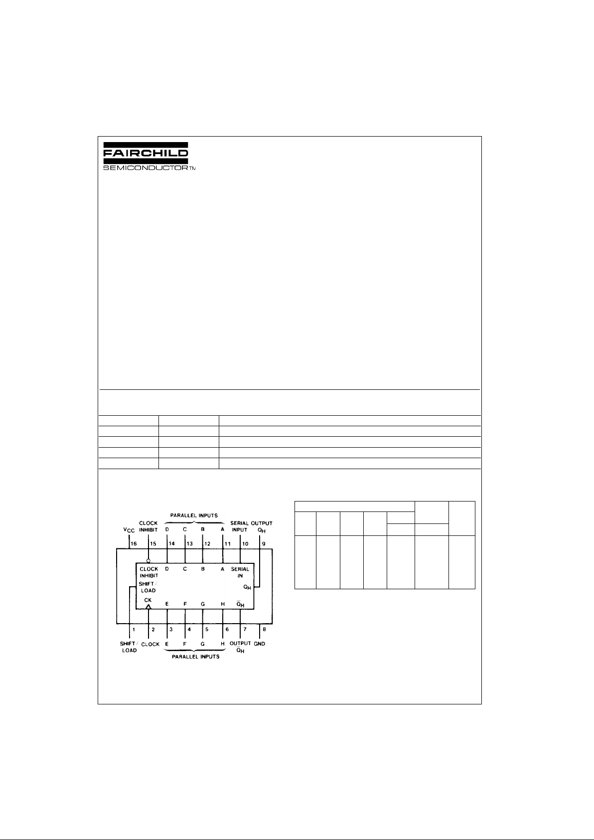
Connection Diagram
Pin Assignments f or DIP, SOIC, SOP and TSSOP
Top View
Function Table
H = HIGH Level (steady state), L = LOW Level (steady state)
X = Irrelevant (any input, inc luding transitions)
↑ = Transition from LOW-to-HIGH level
Q
A0
, QB0, QH0 = The lev el of QA, QB, or QH, respectively, before the indi-
cated steady-stat e input conditions were es t ablished.
Q
AN
, QGN = The level of QA or QG before the most recent ↑ transition of the
clock; indicates a one-bit shift.
Order Number Package Number Package Description
MM74HC165M M16A 16-Lead Small Outline Integrated Circuit (SOIC), JEDEC MS-012, 0.150” Narrow
MM74HC165SJ M16D 16-Lead Small Outline Package (SOP), EIAJ TYPE II, 5.3mm Wide
MM74HC165MTC MTC16 16-Lead Thin Shrink Small Outline Package (TSSOP), JEDEC MO-153, 4.4mm Wide
MM74HC165 N16E 16-Lead Plastic Dual-In-Line Package (PDIP), JEDEC MS-001, 0.300” Wide
Inputs Internal Output
Shift/ Clock
Clock Serial
Parallel
Outputs
Q
H
Load Inhibit
A. . .H Q
AQB
LXXXa...habh
HL LX XQ
A0QB0QH0
HL ↑ HXHQANQ
GN
HL ↑ LXLQANQ
GN
HHXX XQA0QB0Q
H0
Page 2
www.fairchildsemi.com 2
MM74HC165
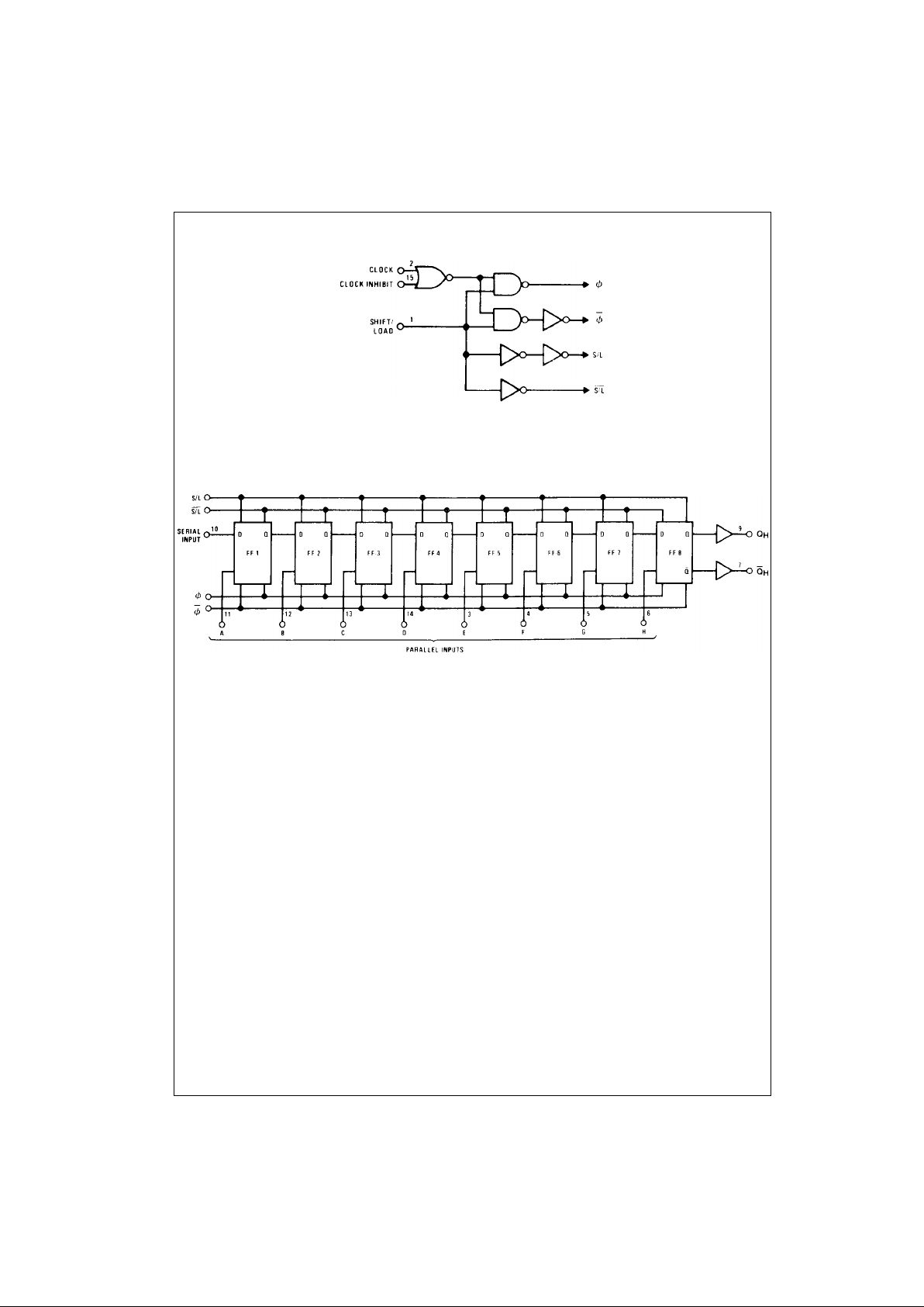
Logic Diagrams
Page 3
3 www.fairchildsemi.com
MM74HC165
Absolute Maximum Ratings(Note 1)
(Note 2)
Recommended Operating
Conditions
Note 1: Absolute Maximum Ra tings are those valu es beyond w hich dam-
age to the device may occur.
Note 2: Unless otherwise specified all voltages are referenced to ground.
Note 3: Power Dissipation te mperature d erating — pl astic “N” pa ckage: −
12 mW/°C from 65°C to 85°C.
DC Electrical Characteristics (Note 4)
Note 4: For a powe r supply o f 5V ±10% the worst case output voltages (VOH, and VOL) occur for HC at 4.5V. Thus the 4. 5V valu es shou ld be u sed when
designing with this supply. Worst case V
IH
and VIL occur at V
CC
= 5.5V and 4.5V respectively. (The VIH value at 5.5V is 3 .8 5V.) The worst c as e leakage cur-
rent (I
IN
, ICC, and IOZ) occur for CMOS at the higher voltage and so th e 6. 0V values should be used.
Supply Voltage (VCC) −0.5 to +7.0V
DC Input Voltage (V
IN
) −1.5 to V
CC
+1.5V
DC Output Voltage (V
OUT
) −0.5 to V
CC
+0.5V
Clamp Diode Current (I
IK
, IOK) ±20 mA
DC Output Current, per pin (I
OUT
) ±25 mA
DC V
CC
or GND Current, per pin (ICC) ±50 mA
Storage Temperature Range (T
STG
) −65°C to +150°C
Power Dissipation (P
D
)
(Note 3) 600 mW
S.O. Package only 500 mW
Lead Temperature (T
L
)
(Solderi ng 10 seconds) 260°C
Min Max Units
Supply Voltage (V
CC
)26V
DC Input or Output Voltage
(V
IN
, V
OUT
)0V
CC
V
Operating Temperature Range (T
A
) −40 +85 °C
Input Rise or Fall Times
(t
r
, tf) V
CC
= 2.0V 1000 ns
V
CC
= 4.5V 500 ns
V
CC
= 6.0V 400 ns
Symbol Parameter Conditions
V
CC
TA = 25°CTA = −40 to 85°CTA = −55 to 125°C
Units
Typ Guaranteed Limits
V
IH
Minimum HIGH Level 2.0V 1.5 1.5 1.5 V
Input Voltage 4.5V 3.15 3.15 3.15 V
6.0V 4.2 4.2 4.2 V
V
IL
Maximum LOW Level 2.0V 0.5 0.5 0.5 V
Input Voltage 4.5V 1.35 1.35 1.35 V
6.0V 1.8 1.8 1.8 V
V
OH
Minimum HIGH Level V
IN
= VIH or V
IL
Output Voltage |I
OUT
| ≤ 20 µA 2.0V 2.0 1.9 1.9 1.9 V
4.5V 4.5 4.4 4.4 4.4 V
6.0V 6.0 5.9 5.9 5.9 V
V
IN
= VIH or V
IL
|I
OUT
| ≤ 4.0 mA 4.5V 4.2 3.98 3.84 3.7 V
|I
OUT
| ≤ 5.2 mA 6.0V 5.7 5.48 5.34 5.2 V
V
OL
Maximum LOW Level V
IN
= VIH or V
IL
Output Voltage |I
OUT
| ≤ 20 µA 2.0V 0 0.1 0.1 0.1 V
4.5V 0 0.1 0.1 0.1 V
6.0V 0 0.1 0.1 0.1 V
V
IN
= VIH or V
IL
|I
OUT
| ≤ 4.0 mA 4.5V 0.2 0.26 0.33 0.4 V
|I
OUT
| ≤ 5.2 mA 6.0V 0.2 0.26 0.33 0.4 V
I
IN
Maximum Input V
IN
= VCC or GND 6.0V ±0.1 ±1.0 ±1.0 µA
Current V
CC
= 2−6V
I
CC
Maximum Quiescent V
IN
= VCC or GND 6.0V 8.0 80 160 µA
Supply Current I
OUT
= 0 µA
V
CC
= 2−6V
Page 4

www.fairchildsemi.com 4
MM74HC165
AC Electrical Characteristics
V
CC
= 5V, T
A
= 25°C, C
L
= 15 pF, tr = t
f
= 6 ns
AC Electrical Characteristics
CL = 50 pF, t
r
= t
f
= 6 ns (unless otherwise specified)
Symbol Parameter Conditions Typ
Guaranteed
Limit
Units
f
MAX
Maximum Operating Frequency 50 30 MHz
t
PHL
, t
PLH
Maximum Propagation Delay H to QH or Q
H
15 25 ns
t
PHL
, t
PLH
Maximum Propagation Delay 13 25 ns
Serial Shift/Parallel Load to Q
H
t
PHL
, t
PLH
Maximum Propagation Delay 15 25 ns
Clock to Output
t
S
Minimum Setup Time Serial Input 10 20 ns
to Clock, Parallel or Data to Shift/Load
t
S
Minimum Setup Time Shift/Load to Clock 11 20 ns
t
S
Minimum Setup Time Clock Inhibit to Clock 10 20 ns
t
H
Minimum Hold Time Serial 0ns
Input to Clock or
Parallel Data to Shift/Load
t
W
Minimum Pulse Width Clock 16 ns
Symbol Parameter Conditions
V
CC
TA = 25°CTA = −40 to 85°CTA = −55 to 125°C
Units
Typ Guaranteed Limits
f
MAX
Maximum Operating 2.0V 10 5 4 4 MHz
Frequency 4.5V 45 27 21 18 MHz
6.0V 50 32 25 21 MHz
t
PHL
, t
PLH
Maximum Propagation 2.0V 70 150 189 225 ns
Delay H to QH or Q
H
4.5V 21 30 38 45 ns
6.0V 18 26 33 39 ns
t
PHL
, t
PLH
Maximum Propagation 2.0V 70 175 220 260 ns
Delay Serial Shift/ 4.5V 21 35 44 52 ns
Parallel Load to Q
H
6.0V 18 30 37 44 ns
t
PHL
, t
PLH
Maximum Propagation 2.0V 70 150 189 225 ns
Delay Clock to Output 4.5V 21 30 38 45 ns
6.0V 18 26 33 39 ns
t
S
Minimum Setup Time 2.0V 35 100 125 150 ns
Serial Input to Clock, 4.5V 11 20 25 30 ns
or Parallel Data to Shift/Load 6.0V 9 17 21 25 ns
t
S
Minimum Setup Time 2.0V 38 100 125 150 ns
Shift/Load to Clock 4.5V 12 20 25 30 ns
6.0V 9 17 21 25 ns
t
S
Minimum Setup Time 2.0V 35 100 125 150 ns
Clock Inhibit to Clock 4.5V 11 20 25 30 ns
6.0V 9 17 21 25 ns
t
H
Minimum Hold Time Serial 2.0V 0 0 0 ns
Input to Clock or 4.5V 0 0 0 ns
Parallel Data to Shift/Load 6.0V 0 0 0 ns
t
W
Minimum Pulse Width, 2.0V 30 80 100 120 ns
Clock 4.5V 9 16 20 24 ns
6.0V 8 14 18 20 ns
t
THL
, t
TLH
Maximum Output 2.0V 30 75 95 110 ns
Rise and Fall Time 4.5V 9 15 19 22 ns
6.0V 8 13 16 19 ns
tr, t
f
Maximum Input Rise and 2.0V 1000 1000 1000 ns
Fall Time 4.5V 500 500 500 ns
6.0V 400 400 400 ns
Page 5

5 www.fairchildsemi.com
MM74HC165
AC Electrical Characteristics (Continued)
Note 5: CPD determines the no load dynamic power con s um ption, PD = CPD V
CC
2
f + ICC VCC, and the no load dynam ic cu rrent consumption,
I
S
= CPDVCCf + ICC.
Symbol Parameter Conditions
V
CC
TA = 25°CTA = −40 to 85°CTA = −55 to 125°C
Units
Typ Guaranteed Limits
C
PD
Power Dissipation (per package) 100 pF
Capacitance (Note 5)
C
IN
Maximum Input Capacitance 5 10 10 10 pF
Page 6

www.fairchildsemi.com 6
MM74HC165
Physical Dimensions inches (millimeters) unless otherwise noted
16-Lead Small Outline Integrated Circuit (SOIC), JEDEC MS-012, 0.150” Narrow
Package Number M16A
16-Lead Small Outline Package (SOP), EIAJ TYPE II, 5.3mm Wide
Package Number M16D
Page 7

7 www.fairchildsemi.com
MM74HC165
Physical Dimensions inches (millimeters) unless otherwise noted (Continued)
16-Lead Thin Shrink Small Outline Package (TSSOP), JEDEC MO-153, 4.4mm Wide
Package Number MTC16
Page 8

Fairchild does not assume any responsibility for use of any circuitry described, no circuit patent licenses are implied and Fairchild reserves the right at any time without notice to change said circuitry and specifications.
MM74HC165 Parallel-in/Serial-out 8-Bit Shift Register
LIFE SUPPORT POLICY
FAIRCHILD’S PRODUCTS ARE NOT AUTHORIZED FOR USE AS CRITICAL COMPONENTS IN LIFE SUPPORT
DEVICES OR SYSTEMS WITHOUT THE EXPRESS WRITTEN APPROVAL OF THE PRESIDENT OF FAIRCHILD
SEMICONDUCTOR CORPORATION. As used herein:
1. Life support de vices o r syste ms are device s or systems
which, (a) are intended for surgical implant into the
body, or (b) support or sustain life, and (c) whose failure
to perform when properly used in accordance with
instructions for use provided in the labeling, can be reasonably expected to result in a significant inju ry to the
user.
2. A critical compon ent in any com ponen t of a life su pport
device or system whose failu re to perform can be reasonably expected to ca use the fa i lure of the life su pp ort
device or system, or to affect its safety or effectiveness.
www.fairchildsemi.com
Physical Dimensions inches (millimeters) unless otherwise noted (Continued)
16-Lead Plastic Dual-In-Line Package (PDIP), MS-001, 0.300” Wide
Package N16E
 Loading...