

Page 1
October 1987
Revised February 1999
MM74HC148 8-3 Line Priority Encoder
© 1999 Fairchild Semiconductor Corporation DS009390.prf www.fairchildsemi.com
MM74HC148
8-3 Line Priority Encoder
General Description
The MM74HC148 priority encoder utilizes advanced silicon-gate CMOS technology. It has the high noise immunity
and low power consumption typical of CMO S circuits, as
well as the s peeds and output drive similar to LB-TTL.
This priority encode r ac cepts 8 input request li ne s 0– 7 a nd
outputs 3 lines A0–A2. The priority encoding ensur es that
only the highest order data li ne is e ncoded . Cascad ing c ircuitry (enable input EI and enable output EO) has been
provided to allow octal expansion without the need for
external circuitry. All data inputs an d outputs are act ive at
the low logic level.
All inputs are protected from damage due to static discharge by internal diod e clamps to V
CC
and ground.
Features
■ Typical propagation delay: 13 ns
■ Wide supply voltage range: 2V–6V
Ordering Code:
Devices also availab le in Tape and Reel. Specify by appending th e s uffix let t er “X” to the ordering cod e.
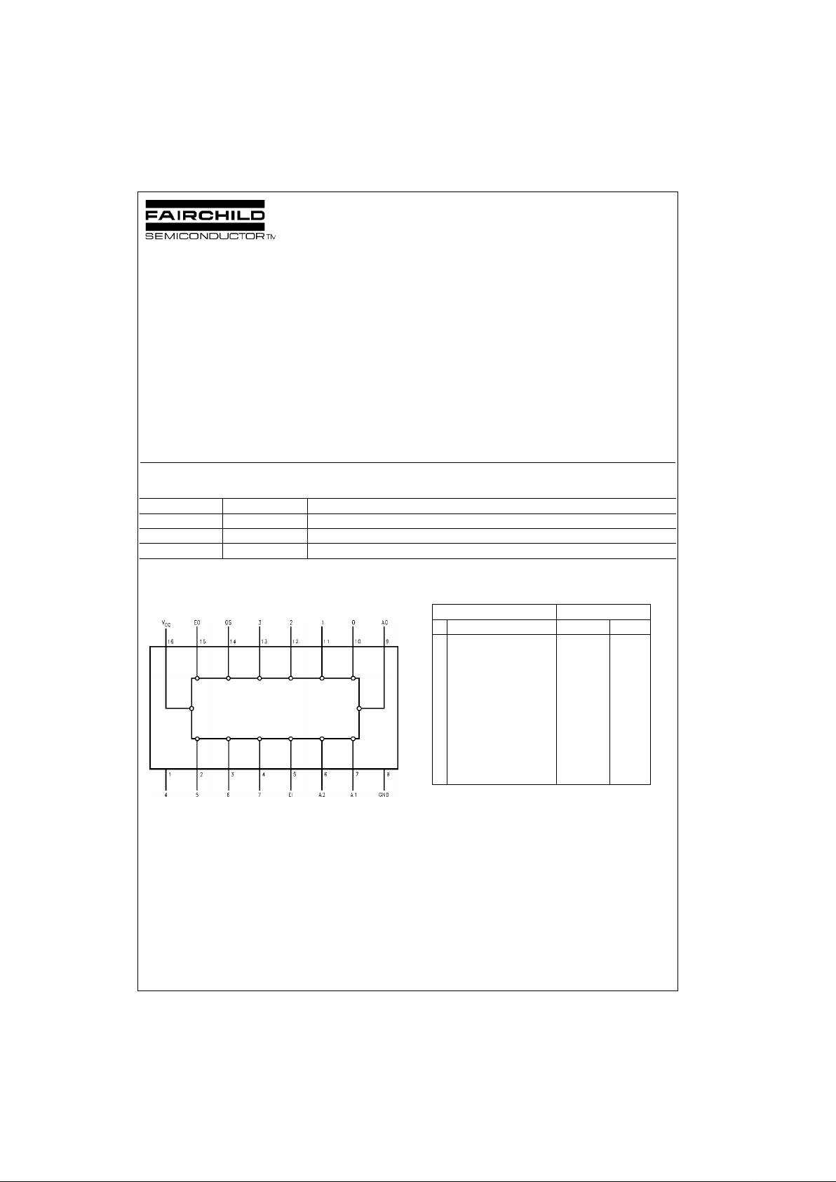
Connection Diagram
Pin Assignments for DIP, SOIC and TSSOP
Truth Table
H = HIGH
L = LOW
X = Irrelevant
Order Number Package Number Package Description
MM74HC148M M16A 16-Lead Small Outline Integrated Circuit (SOIC), JEDEC MS-012, 0.150” Narrow
MM74HC148MTC MTC16 16-Lead Thin Shrink Small Outline Package (TSSOP), JEDEC MO-153, 4.4mm Wide
MM74HC148N N16E 16-Lead Plastic Dual-In-Line Package (PDIP), JEDEC MS-001, 0.300” Wide
Inputs Outputs
EI01234567A2A1A0GSEO
HXXXXXXXXH H H H H
LHHHHHHHH H H H H L
LXXXXXXXL L L L L H
LXXXXXXLH L L H L H
LXXXXXLHH L H L L H
LXXXXLHHHL H H L H
LXXXLHHHHH L L L H
LXXLHHHHH H L H L H
LXLHHHHHH H H L L H
L LHHHHHHH H H H L H
Page 2
www.fairchildsemi.com 2
MM74HC148
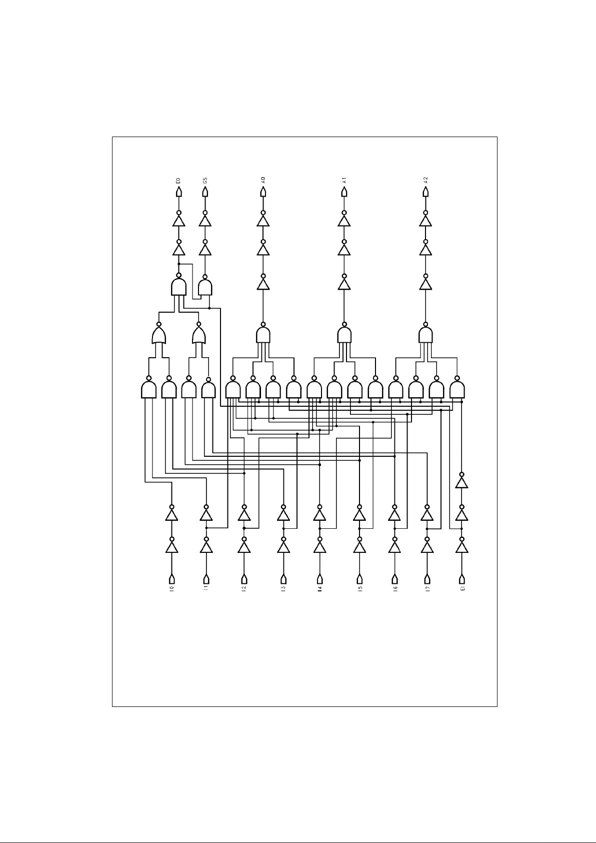
Schematic Diagram
Page 3
3 www.fairchildsemi.com
MM74HC148
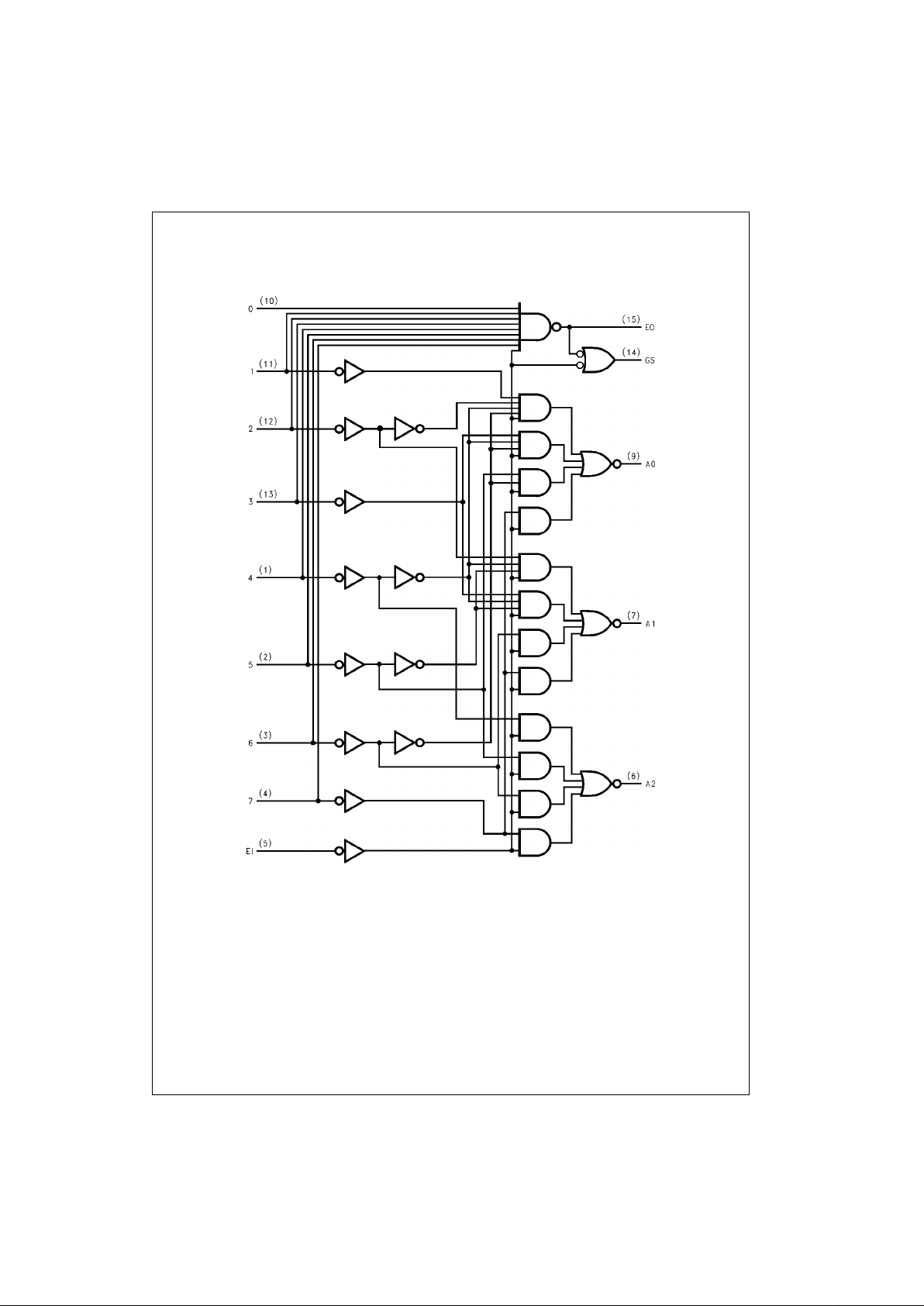
Logic Diagram
Page 4
www.fairchildsemi.com 4
MM74HC148
Absolute Maximum Ratings(Note 1)
(Note 2)
Recommended Operation
Conditions
Note 1: Absolute Maximum Ratings are those values beyond which dam-
age to the device may occur.
Note 2: Unless otherwise specified all voltages are referenced to ground.
Note 3: Power Dissipation temperature derating—plastic “N” package: −12
mW/°C from 65°C to 85°C.
DC Electrical Characteristics (Note 4)
Note 4: For a power supply of 5V ±1 0% the worst c ase ou tput volta ges (VOH, and VOL) occur for HC at 4.5V. Thus the 4. 5V valu es shoul d be use d when
designing with this supply. Worst case V
IH
and VIL occur at VCC = 5.5V and 4.5V respectively. (The VIH value at 5.5V is 3.85V.) The worst case leakage cur-
rent (I
IN
, ICC, and IOZ) occur for CMOS at the higher voltage and so th e 6. 0V values should be used.
Supply Voltage (VCC) −0.5 to +7.0V
DC Input Voltage (V
IN
) −1.5 to VCC +1.5V
DC Output Voltage (V
OUT
) −0.5 to VCC +0.5V
Clamp Diode Current (I
IK
, IOK) ±20 mA
DC Output Current, per pin (I
OUT
) ±25 mA
DC V
CC
or GND Current, per pin (ICC) ±50 mA
Storage Temperature Range (T
STG
) −65°C to +150°C
Power Dissipation (P
D
)
(Note 3) 600 mW
S.O. Package only 500 mW
Lead Temperature (T
L
)
(Soldering 10 seconds) 260°C
Min Max Units
Supply Voltage (V
CC
)26V
DC Input or Output Voltage
(V
IN
, V
OUT
)0V
CC
V
Operating Temperature Range (T
A
)
−40 +85 °C
Input Rise or Fall Times
(t
r
, tf) VCC = 2.0V 1000 ns
V
CC
= 4.5V 500 ns
V
CC
= 6.0V 400 ns
Symbol Parameter Conditions
V
CC
TA = 25°CTA = −40 to 85°CTA = −55 to 125°C
Units
Typ Guaranteed Limits
V
IH
Minimum HIGH Level 2.0V 1.5 1.5 1.5 V
Input Voltage 4.5V 3.15 3.15 3.15 V
6.0V 4.2 4.2 4.2 V
V
IL
Maximum LOW Level 2.0V 0.5 0.5 0.5 V
Input Voltage 4.5V 1.35 1.35 1.35 V
6.0V 1.8 1.8 1.8 V
V
OH
Minimum HIGH Level VIN = VIH or V
IL
Output Voltage |I
OUT
| ≤ 20 µA 2.0V 2.0 1.9 1.9 1.9 V
4.5V 4.5 4.4 4.4 4.4 V
6.0V 6.0 5.9 5.9 5.9 V
VIN = VIH or V
IL
|I
OUT
| ≤ 4.0 mA 4.5V 4.7 3.96 3.84 3.7 V
|I
OUT
| ≤ 5.2 mA 6.0V 5.2 5.48 5.34 5.2 V
V
OL
Maximum LOW Level VIN = VIH or V
IL
Output Voltage |I
OUT
| ≤ 20 µA 2.0V 0 0.1 0.1 0.1 V
4.5V 0 0.1 0.1 0.1 V
6.0V 0 0.1 0.1 0.1 V
VIN = VIH or V
IL
|I
OUT
| ≤ 4.0 mA 4.5V 0.2 0.26 0.33 0.4 V
|I
OUT
| ≤ 5.2 mA 6.0V 0.2 0.26 0.33 0.4 V
I
IN
Maximum Input VIN = VCC or GND 6.0V ±0.1 ±1.0 ±1.0 µA
Current
I
CC
Maximum Quiescent VIN = VCC or GND 6.0V 8.0 80 160 µA
Supply Current I
OUT
= 0 µA
Page 5

5 www.fairchildsemi.com
MM74HC148
AC Electrical Characteristics
AC Electrical Characteristics
VCC = 2.0V to 6.0V, CL = 50 pF, tr = tf = 6 ns (unless otherwise specified)
Note 5: Cpd determines the no lo ad dynamic power con s um ption, and the no load d y namic current consu m pt ion.
Symbol Parameter Conditions Typ
Guaranteed
Limits
Units
t
PHL
, t
PLH
Maximum Propagation Delay, 14 ns
Any Input to Any Output
Symbol Parameter Conditions
V
CC
TA = 25°CTA = −40°C to +85°CTA = −55°C to +125°C
Units
Typ Guaranteed Limits
t
PHL
, t
PLH
Inputs 0–7 2.0V 140 175 210 ns
to Outputs 4.5V 14 28 35 42 ns
A0, A1, A2 6.0V 24 30 36 ns
t
PHL
, t
PLH
Inputs 0–7 2.0V 140 175 210 ns
to 4.5V 15 28 35 42 ns
Output EO 6.0V 24 30 36 ns
t
PHL
, t
PLH
Inputs 0–7 2.0V 160 200 240 ns
to 4.5V 17 32 40 48 ns
Output GS 6.0V 27 34 41 ns
t
PHL
, t
PLH
Input EI 2.0V 160 200 240 ns
to Outputs 4.5V 17 32 40 48 ns
A0, A1, A2 6.0V 27 34 41 ns
t
PHL
, t
PLH
Input EI 2.0V 100 125 150 ns
to 4.5V 12 20 25 30 ns
Output GS 6.0V 17 21 26 ns
t
PHL
, t
PLH
Input EI 2.0V 100 125 150 ns
to 4.5V 12 20 25 30 ns
Output EO 6.0V 17 21 26 ns
tf, t
r
Maximum 2.0V 75 95 110 ns
Output Rise 4.5V 7 15 19 22 ns
and Fall Time 6.0V 13 16 19 ns
C
pd
Power Dissipation 52 pF
Capacitance (Note 5)
C
in
Maximum Input 5 10 10 10 pF
Capacitance
Page 6

www.fairchildsemi.com 6
MM74HC148
Physical Dimensions inches (millimeters) unless otherwise noted
16-Lead Small Outline Integrated Circuit (SOIC), JEDEC MS-012, 0.150” Narrow
Package Number M16A
Page 7

7 www.fairchildsemi.com
MM74HC148
Physical Dimensions inches (millimeters) unless otherwise noted (Continued)
16-Lead Thin Shrink Small Outline Package (TSSOP), JEDEC MO-153, 4.4mm Wide
Package Number MTC16
Page 8
Fairchild does not assume any responsibility for use of any circuitry described, no circuit patent licenses are implied and Fairchild reserves the right at any time without notice to change said circuitry and specifications.
MM74HC148 8-3 Line Priority Encoder
LIFE SUPPORT POLICY
FAIRCHILD’S PRODUCTS ARE NOT AUTHORIZED FOR USE AS CRITICAL COMPONENTS IN LIFE SUPPORT
DEVICES OR SYSTEMS WITHOUT THE EXPRESS WRITTEN APPROVAL OF THE PRESIDENT OF FAIRCHILD
SEMICONDUCTOR CORPORATION. As used herein:
1. Life support devices o r systems a re devices or syste ms
which, (a) are intended for surgical implant into the
body, or (b) support or sustain life, and (c) whose failure
to perform when properly used in accordance with
instructions for use provided in the labeling, can be reasonably expected to result in a significant inju ry to the
user.
2. A critical compon ent i n any compon ent of a lif e support
device or system whose failu re to perform can be reasonably expected to ca use the fa i lure of the life su pp ort
device or system, or to affect its safety or effectiveness.
www.fairchildsemi.com
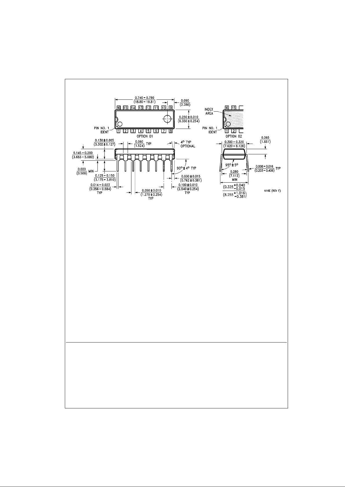
Physical Dimensions inches (millimeters) unless otherwise noted (Continued)
16-Lead Plastic Dual-In-Line Package (PDIP), JEDEC MS-001, 0.300” Wide
Package Number N16E
 Loading...