

Datasheet MM74HC139MTC, MM74HC139MX, MM74HC139N, MM74HC139SJ, MM74HC139M Datasheet (Fairchild Semiconductor)
...Page 1
September 1983
Revised February 1999
MM74HC139 Dual 2-To-4 Line Decoder
© 1999 Fairchild Semiconductor Corporation DS005311.prf www.fairchildsemi.com
MM74HC139
Dual 2-To-4 Line Decoder
General Description
The MM74HC139 decoder utilizes advanced silicon-gate
CMOS technology, and is well suite d to memory address
decoding or data routing applications. It possesses the
high noise immunity and l ow power consumption usually
associated with CMOS circuitry, yet has speeds compar able to low power Schottky TTL logic.
The MM74HC139 contain two independent one-of-four
decoders each with a single active low enable input (G1, or
G2). Data on the select inputs (A 1, and B1 or A2, an d B2)
cause one of the four normally high outputs to go LOW.
The decoder’s outputs can drive 10 low power Schottky
TTL equivalent lo ads, and are functionally a s well as pin
equivalent to the 74LS 139. All inputs are protected from
damage due to static discharge by diodes to V
CC
and
ground.
Features
■ Typical propagation delays —
Select to outputs (4 delays): 18 ns
Select to output (5 delays): 28 ns
Enable to output: 20 ns
■ Low power: 40 µW quiescent s upply power
■ Fanout of 10 LS-TTL devices
■ Input current maximum 1 µA, typical 10 pA
Ordering Code:
Devices also availab le in Tape and Reel. Specify by appending th e s uffix let t er “X” to the ordering cod e.
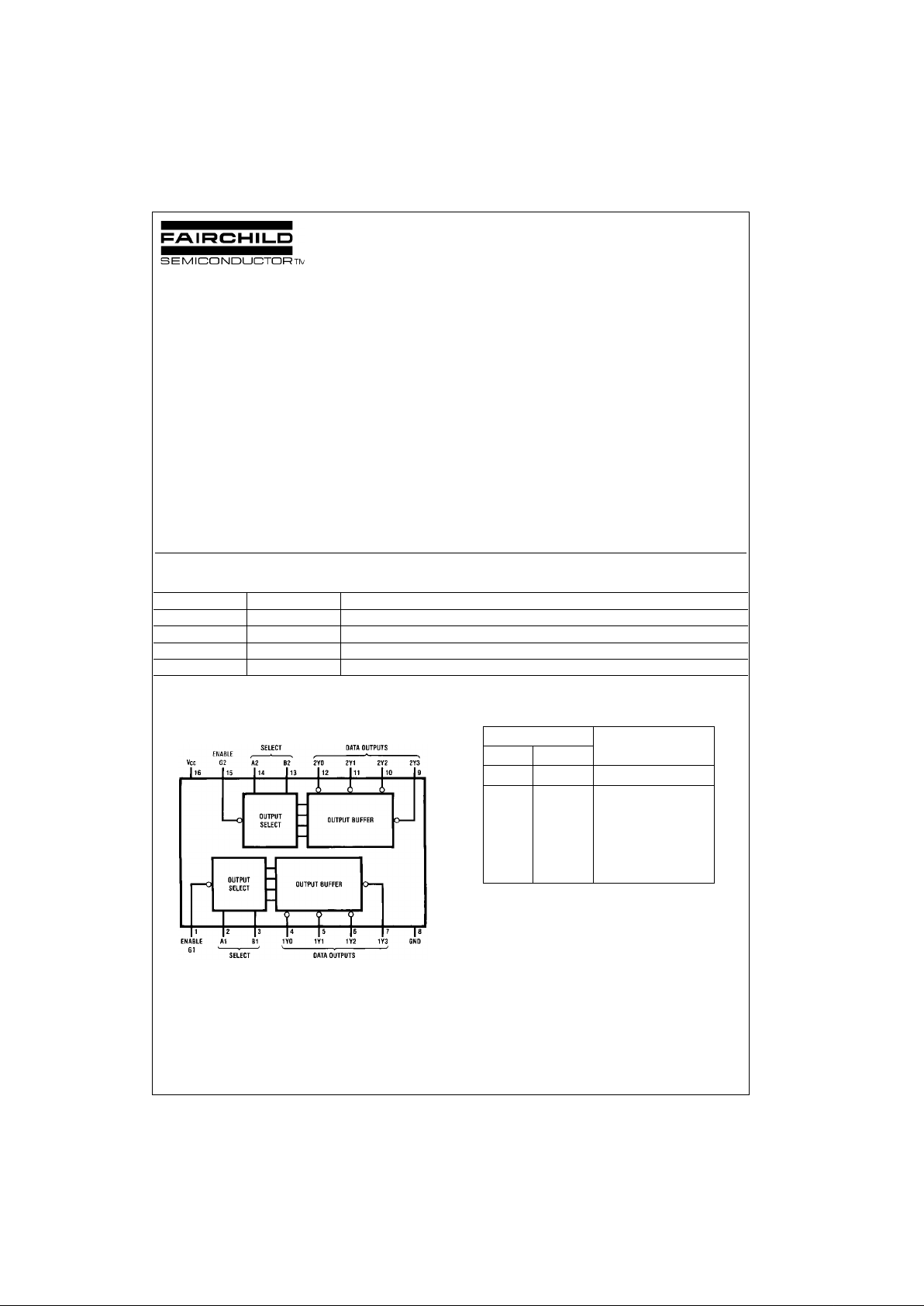
Connection Diagram
Pin Assignments f or DIP, SOIC, SOP and TSSOP
Truth Table
H = HIGH Level
L = LOW Level
X = Don't Care
Order Number Package Number Package Description
MM74HC139M M16A 16-Lead Small Outline Integrated Circuit (SOIC), JEDEC MS-012, 0.150” Narrow
MM74HC139SJ M16D 16-Lead Small Outline Package (SOP), EIAJ TYPE II, 5.3mm Wide
MM74HC139MTC MTC16 16-Lead Thin Shrink Small Outline Package (TSSOP) JEDEC MO-153, 4.4mm Wide
MM74HC139N N16E 16-Lead Plastic Dual-In-Line Package (PDIP), JEDEC MS-001, 0.300” Wide
Inputs Outputs
Enable Select
G B A Y0Y1Y2Y3
H XXHHHH
LLLLHHH
LLHHLHH
LHLHHLH
L HHHHHL
Page 2

www.fairchildsemi.com 2
MM74HC139
Logic Diagram
(1 of 2)
Page 3
3 www.fairchildsemi.com
MM74HC139
Absolute Maximum Ratings(Note 1)
(Note 2)
Recommended Operating
Conditions
Note 1: Absolute Maximum Ra tings are those valu es beyond w hich dam-
age to the device may occur.
Note 2: Unless otherwise specified all voltages are referenced to ground.
Note 3: Power Dissipation te mperature d erating — pl astic “N” pa ckage: −
12 mW/°C from 65°C to 85°C.
DC Electrical Characteristics (Note 4)
Note 4: For a powe r supply o f 5V ±10% the worst case output voltages (VOH, and VOL) occur for HC at 4.5V. Thus the 4. 5V valu es shou ld be u sed when
designing with this supply. Worst case V
IH
and VIL occur at V
CC
= 5.5V and 4.5V respectively. (The VIH value at 5.5V is 3 .8 5V.) The worst c as e leakage cur-
rent (I
IN
, ICC, and IOZ) occur for CMOS at the higher voltage and so th e 6. 0V values should be used.
Supply Voltage (VCC) −0.5 to +7.0V
DC Input Voltage (V
IN
) −1.5 to V
CC
+1.5V
DC Output Voltage (V
OUT
) −0.5 to V
CC
+0.5V
Clamp Diode Current (I
IK
, IOK) ±20 mA
DC Output Current, per pin (I
OUT
) ±25 mA
DC V
CC
or GND Current, per pin (ICC) ±50 mA
Storage Temperature Range (T
STG
) −65°C to +150°C
Power Dissipation (P
D
)
(Note 3) 600 mW
S.O. Package only 500 mW
Lead Temperature (T
L
)
(Solderi ng 10 seconds) 260°C
Min Max Units
Supply Voltage (V
CC
)26V
DC Input or Output Voltage 0 V
CC
V
(V
IN
, V
OUT
)
Operating Temperature Range (T
A
) −40 +85 °C
Input Rise or Fall Times
(t
r
, tf) V
CC
= 2.0V 1000 ns
V
CC
= 4.5V 500 ns
V
CC
= 6.0V 400 ns
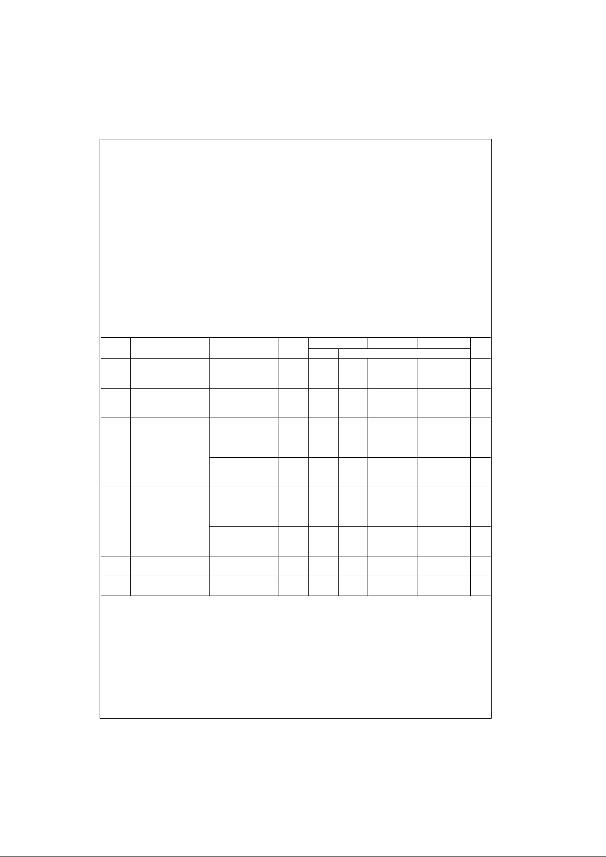
Symbol Parameter Conditions
V
CC
TA = 25°CTA = −40 to 85°CTA = −55 to 125°C
Units
Typ Guaranteed Limits
V
IH
Minimum HIGH Level 2.0V 1.5 1.5 1.5 V
Input Voltage 4.5V 3.15 3.15 3.15 V
6.0V 4.2 4.2 4.2 V
V
IL
Maximum LOW Level 2.0V 0.5 0.5 0.5 V
Input Voltage 4.5V 1.35 1.35 1.35 V
6.0V 1.8 1.8 1.8 V
V
OH
Minimum HIGH Level V
IN
= VIH or V
IL
Output Voltage |I
OUT
| ≤ 20 µA 2.0V 2.0 1.9 1.9 1.9 V
4.5V 4.5 4.4 4.4 4.4 V
6.0V 6.0 5.9 5.9 5.9 V
V
IN
= VIH or V
IL
|I
OUT
| ≤ 4.0 mA 4.5V 4.2 3.98 3.84 3.7 V
|I
OUT
| ≤ 5.2 mA 6.0V 5.7 5.48 5.34 5.2 V
V
OL
Maximum LOW Level V
IN
= VIH or V
IL
Output Voltage |I
OUT
| ≤ 20 µA 2.0V 0 0.1 0.1 0.1 V
4.5V 0 0.1 0.1 0.1 V
6.0V 0 0.1 0.1 0.1 V
V
IN
= VIH or V
IL
|I
OUT
| ≤ 4.0 mA 4.5V 0.2 0.26 0.33 0.4 V
|I
OUT
| ≤ 5.2 mA 6.0V 0.2 0.26 0.33 0.4 V
I
IN
Maximum Input V
IN
= VCC or GND 6.0V ±0.1 ±1.0 ±1.0 µA
Current
I
CC
Maximum Quiescent V
IN
= VCC or GND 6.0V 8.0 80 160 µA
Supply Current I
OUT
= 0 µA
Page 4

www.fairchildsemi.com 4
MM74HC139
AC Electrical Characteristics
V
CC
= 5V, TA = 25°C, CL = 15 pF, tr = t
f
= 6 ns
AC Electrical Characteristics
C
L
= 50 pF, tr = t
f
= 6 ns (unless otherwise specified)
Note 5: 4 levels of delay are A to Y1, Y3 and B to Y2, Y3.
Note 6: 5 levels of delay are A to Y0, Y2 and B to Y0, Y1.
Note 7: CPD determines the no lo ad dynamic power con s um ption, PD = CPD V
CC
2
f + ICC VCC, and the no load dynamic current consum pt ion,
I
S
= CPDVCCf + ICC.
Symbol Parameter Conditions T yp
Guaranteed
Units
Limit
t
PHL
, t
PLH
Maximum Propagation 18 30 ns
Delay, Binary Select to any Output
4 levels of delay
t
PHL
, t
PLH
Maximum Propagation 28 38 ns
Delay, Binary Select to any Output
5 levels of delay
t
PHL
, t
PLH
Maximum Propagation 19 30 ns
Delay, Enable to any Output
Symbol Parameter Conditions
V
CC
TA = 25°CTA = −40 to 85°CTA = −55 to 125°C
Units
Typ Guaranteed Limits
t
PHL
, t
PLH
Maximum Propagation (Note 5) 2.0V 110 175 219 254 ns
Delay Binary Select to 4.5V 22 35 44 51 ns
any Output 4 levels of delay 6.0V 18 30 38 44 ns
t
PHL
, t
PLH
Maximum Propagation (Note 6) 2.0V 165 220 275 320 ns
Delay Binary Select to any 4.5V 33 44 55 64 ns
Output 5 levels of delay 6.0V 28 38 47 54 ns
t
PHL
, t
PLH
Maximum Propagation 2.0V 115 175 219 254 ns
Delay Enable to any 4.5V 23 35 44 51 ns
Output 6.0V 19 30 38 44 ns
t
TLH
, t
TLH
Maximum Output Rise 2.0V 30 75 95 110 ns
and Fall Time 4.5V 8 15 19 22 ns
6.0V 7 13 16 19 ns
C
IN
Maximum Input 3 10 10 10 pF
Capacitance
C
PD
Power Dissipation (Note 7) 75 pF
Capacitance (Note 7)
Page 5

5 www.fairchildsemi.com
MM74HC139
Physical Dimensions inches (millimeters) unless otherwise noted
16-Lead Small Outline Integrated Circuit (SOIC), JEDEC MS-012, 0.150” Narrow
Package Number M16A
16-Lead Small Outline Package (SOP) EIAJ TYPE II, 5.3mm Wide
Package Number M16D
Page 6

www.fairchildsemi.com 6
MM74HC139
Physical Dimensions inches (millimeters) unless otherwise noted (Continued)
16-Lead Thin Shrink Small Outline Package (TSSOP), JEDEC MO-153, 4.4mm Wide
Package Number MTC16
Page 7

Fairchild does not assume any responsibility for use of any circuitry described, no circuit patent licenses are implied and Fairchild reserves the right at any time without notice to change said circuitry and specifications.
MM74HC139 Dual 2-To-4 Line Decoder
LIFE SUPPORT POLICY
FAIRCHILD’S PRODUCTS ARE NOT AUTHORIZED FOR USE AS CRITICAL COMPONENTS IN LIFE SUPPORT
DEVICES OR SYSTEMS WITHOUT THE EXPRESS WRITTEN APPROVAL OF THE PRESIDENT OF FAIRCHILD
SEMICONDUCTOR CORPORATION. As used herein:
1. Life sup por t de vices o r syst ems are devices or systems
which, (a) are intended for surgical implant into the
body, or (b) support or sustain life, and (c) whose failure
to perform when properly used in accordance with
instructions for use provided i n the labe li ng, can be re asonably expected to result in a significant injury to the
user.
2. A criti cal com ponen t in any compo nent o f a l ife supp ort
device or system whose failu re to perform can b e reasonably expected to c ause th e fa i lure of the li fe s upp or t
device or system, or to affect its safety or effectiveness.
www.fairchildsemi.com
Physical Dimensions inches (millimeters) unless otherwise noted (Continued)
16-Lead Plastic Dual-In-Line Package (PDIP), JEDEC MS-001, 0.300” Wide
Package Number N16E
 Loading...