

Page 1
MM74HC125, MM74HC126 — 3-STATE Quad Buffers
February 2008
MM74HC125, MM74HC126
3-STATE Quad Buffers
Features
■
Typical propagation delay: 13ns
Wide operating voltage range: 2V–6V
■
■
Low input current: 1µA maximum
■
Low quiescent current: 80µA maximum (74HC)
Fanout of 15 LS-TTL loads
■
General Description
The MM74HC125 and MM74HC126 are general purpose 3-STATE high speed non-inverting buffers utilizing
advanced silicon-gate CMOS technology. They have
high drive current outputs which enable high speed operation even when driving large bus capacitances. These
circuits possess the low power dissipation of CMOS
circuitry, yet have speeds comparable to low power
Schottky TTL circuits. Both circuits are capable of driving
up to 15 low power Schottky inputs.
The MM74HC125 require the 3-STATE control input C to
be taken high to put the output into the high impedance
condition, whereas the MM74HC126 require the control
input to be low to put the output into high impedance.
All inputs are protected from damage due to static
discharge by diodes to V
and ground.
CC
Ordering Information
Package
Order Number
MM74HC125M M14A 14-Lead Small Outline Integrated Circuit (SOIC), JEDEC MS-012, 0.150"
MM74HC125SJ M14D 14-Lead Small Outline Package (SOP), EIAJ TYPE II, 5.3mm Wide
MM74HC125MTC MTC14 14-Lead Thin Shrink Small Outline Package (TSSOP), JEDEC MO-153,
MM74HC125N N14A 14-Lead Plastic Dual-In-Line Package (PDIP), JEDEC MS-001, 0.300" Wide
MM74HC126M M14A 14-Lead Small Outline Integrated Circuit (SOIC), JEDEC MS-012, 0.150"
MM74HC126SJ M14D 14-Lead Small Outline Package (SOP), EIAJ TYPE II, 5.3mm Wide
MM74HC126MTC MTC14 14-Lead Thin Shrink Small Outline Package (TSSOP), JEDEC MO-153,
MM74HC126N N14A 14-Lead Plastic Dual-In-Line Package (PDIP), JEDEC MS-001, 0.300" Wide
Device also available in Tape and Reel. Specify by appending suffix letter “X” to the ordering number.
Number Package Description
Narrow
4.4mm Wide
Narrow
4.4mm Wide
All packages are lead free per JEDEC: J-STD-020B standard.
©1983 Fairchild Semiconductor Corporation www.fairchildsemi.com
MM74HC125, MM74HC126 Rev. 1.3.0
Page 2
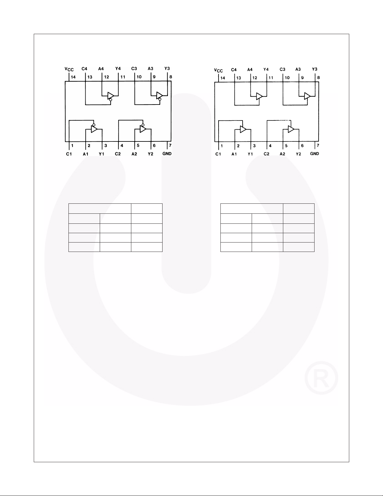
Connection Diagrams
Top View (MM74HC125) Top View (MM74HC126)
MM74HC125, MM74HC126 — 3-STATE Quad Buffers
Pin Assignments for DIP, SOIC, SOP and TSSOP
Truth Tables
ACY
HLH
LLL
XHZ
Inputs Output
Inputs Output
ACY
HHH
LHL
XLZ
MM74HC125 MM74HC126
©1983 Fairchild Semiconductor Corporation www.fairchildsemi.com
MM74HC125, MM74HC126 Rev. 1.3.0 2
Page 3
=
=
=
MM74HC125, MM74HC126 — 3-STATE Quad Buffers
Absolute Maximum Ratings
(1)
Stresses exceeding the absolute maximum ratings may damage the device. The device may not function or be
operable above the recommended operating conditions and stressing the parts to these levels is not recommended.
In addition, extended exposure to stresses above the recommended operating conditions may affect device reliability.
The absolute maximum ratings are stress ratings only.
Symbol Parameter Rating
V
CC
V
IN
V
OUT
, I
I
IK
I
OUT
I
CC
T
STG
P
D
T
Notes:
1. Unless otherwise specified all voltages are referenced to ground.
2. Power Dissipation temperature derating — plastic “N” package: –12mW/°C from 65°C to 85°C.
Supply Voltage –0.5 to +7.0V
DC Input Voltage –1.5 to V
DC Output Voltage –0.5 to V
Clamp Diode Current ±20mA
OK
DC Output Current, per pin 35mA
DC V
or GND Current, per pin ±70mA
CC
Storage Temperature Range –65°C to +150°C
Power Dissipation
Note 2 600mW
S.O. Package only 500mW
Lead Temperature (Soldering 10 seconds) 260°C
L
CC
CC
+1.5V
+0.5V
Recommended Operating Conditions
The Recommended Operating Conditions table defines the conditions for actual device operation. Recommended
operating conditions are specified to ensure optimal performance to the datasheet specifications. Fairchild does not
recommend exceeding them or designing to absolute maximum ratings.
Symbol Parameter Min. Max. Units
V
CC
V
, V
IN
T
A
t
, t
r
Supply Voltage 2 6 V
DC Input or Output Voltage 0 V
OUT
Operating Temperature Range –40 +85 °C
Input Rise or Fall Times
f
V
V
V
2.0V
CC
4.5V 500 ns
CC
6.0V 400 ns
CC
CC
1000 ns
V
©1983 Fairchild Semiconductor Corporation www.fairchildsemi.com
MM74HC125, MM74HC126 Rev. 1.3.0 3
Page 4

=
=
=
=
=
| ≤
=
| ≤
=
| ≤
=
| ≤
=
| ≤
=
| ≤
=
=
=
=
=
=
MM74HC125, MM74HC126 — 3-STATE Quad Buffers
DC Electrical Characteristics
(3)
Symbol Parameter Conditions V
V
V
V
OH
V
OL
I
OZ
I
IN
I
CC
Minimum HIGH
IH
Level Input
Voltage
Maximum LOW
IL
Level Input
Voltage
Minimum HIGH
Level Output
Voltage
Maximum LOW
Level Output
Voltage
Maximum
3-STATE Output
Leakage Current
Maximum Input
Current
Maximum
Quiescent
Supply Current
V
IN
|I
OUT
V
IN
|I
OUT
V
IN
|I
OUT
V
IN
|I
OUT
V
IN
|I
OUT
V
IN
|I
OUT
V
IN
V
OUT
C
n
V
IN
V
IN
I
OUT
V
or V
IH
,
IL
20µA
V
or V
IH
,
IL
6.0mA
V
or V
IH
,
IL
7.8mA
V
or V
IH
,
IL
20µA
V
or V
IH
,
IL
6.0mA
V
or V
IH
,
IL
7.8mA
V
or V
or GND,
CC
,
IL
IH
V
Disabled
V
or GND 6.0 ±0.1 ±1.0 ±1.0 µA
CC
V
or GND,
CC
0µA
T
CC
(V)
–40°C
T
25°C
A
A
to 85°C
T
–40°C
A
to 125°C
UnitsTyp. Guaranteed Limits
2.0 1.5 1.5 1.5 V
4.5 3.15 3.15 3.15
6.0 4.2 4.2 4.2
2.0 0.5 0.5 0.5 V
4.5 1.35 1.35 1.35
6.0 1.8 1.8 1.8
2.0 2.0 1.9 1.9 1.9 V
4.5 4.5 4.4 4.4 4.4
6.0 6.0 5.9 5.9 5.9
4.5 4.2 3.98 3.84 3.7
6.0 5.7 5.48 5.34 5.2
2.0 0 0.1 0.1 0.1 V
4.5 0 0.1 0.1 0.1
6.0 0 0.1 0.1 0.1
4.5 0.2 0.26 0.33 0.4
6.0 0.2 0.26 0.33 0.4
6.0 ±0.5 ±5 ±10 µA
6.0 8.0 80 160 µA
Note:
3. For a power supply of 5V ±10% the worst case output voltages (V
values should be used when designing with this supply. Worst case V
respectively. (The V
value at 5.5V is 3.85V.) The worst case leakage current (I
IH
OH
, and V
and V
IH
) occur for HC at 4.5V. Thus the 4.5V
OL
occur at V
IL
, I
IN
CC
, and I
5.5V and 4.5V
CC
) occur for CMOS at
OZ
the higher voltage and so the 6.0V values should be used.
©1983 Fairchild Semiconductor Corporation www.fairchildsemi.com
MM74HC125, MM74HC126 Rev. 1.3.0 4
Page 5

AC Electrical Characteristics
V
CC
5V, T
25°C, C
A
45pF, t
L
t
6ns
r
f
Symbol Parameter Conditions Typ.
t
PHL
t
PZH
t
PHZ
t
PZL
t
PLZ
, t
Maximum Propagation Delay Time 13 18 ns
PLH
Maximum Output Enable Time to HIGH
RL = 1kΩ 13 25 ns
Level
Maximum Output Disable Time from
RL = 1kΩ, CL = 5pF 17 25 ns
HIGH Level
Maximum Output Enable Time to LOW
RL = 1kΩ 18 25 ns
Level
Maximum Output Disable Time from
RL = 1kΩ, CL = 5pF 13 25 ns
LOW Level
AC Electrical Characteristics
V
2.0V to 6.0V, C
CC
Symbol Parameter V
t
, t
, t
, t
, t
, t
PD
Maximum Propagation
PLH
Delay Time
Maximum Propagation
PHL
Delay Time
Maximum Output
PZL
Enable Time
Maximum Output
PLZ
Disable Time
Maximum Output
PZH
Enable Time
Maximum Output
THL
Rise and Fall Time
Input Capacitance 5 10 10 10 pF
IN
Output Capacitance
Outputs
Power Dissipation
Capacitance
(per gate)
PHL
t
PLH
t
PZH
t
PHZ
t
PZL
t
TLH
C
, t
C
OUT
C
= 50pF, tr = tf = 6ns (unless otherwise specified)
L
TA = 25°C
(V) Conditions
CC
2.0 40 100 125 150 ns
4.5 14 20 25 30
6.0 12 17 21 25
2.0 CL = 150pF 35 130 163 195 ns
4.5 14 26 33 39
6.0 12 22 28 39
2.0 RL = 1kΩ 25 125 156 188 ns
4.5 14 25 31 38
6.0 12 21 26 31
2.0 RL = 1kΩ 25 125 156 188 ns
4.5 14 25 31 38
6.0 12 21 26 31
2.0 CL = 150pF,
R
= 1kΩ
4.5 15 28 35 42
6.0 13 24 30 36
2.0V CL = 50pF 30 60 75 90 ns
4.5V 7 12 15 18
6.0V 6 10 13 15
(4)
L
Enabled 45 pF
Disabled 6
35 140 175 210 ns
15 20 20 20 pF
TA = –40°C
to 85°C
Guaranteed
Limit Units
TA = –40°C
to 125°C
=
=
=
=
=
=
MM74HC125, MM74HC126 — 3-STATE Quad Buffers
UnitsTyp. Guaranteed Limits
Note:
4. C
determines the no load dynamic power consumption, PD = CPD V
PD
current consumption, I
©1983 Fairchild Semiconductor Corporation www.fairchildsemi.com
MM74HC125, MM74HC126 Rev. 1.3.0 5
= CPD VCC f + ICC.
S
2
f + ICC VCC, and the no load dynamic
CC
Page 6

Physical Dimensions
8.75
8.50
7.62
MM74HC125, MM74HC126 — 3-STATE Quad Buffers
A
0.65
6.00
PIN ONE
INDICATOR
1.75 MAX
1.50
1.25
14
1
1.27
(0.33)
8
7
0.51
0.35
0.25
B
4.00
3.80
1.70 1.27
LAND PATTERN RECOMMENDATION
M
BC A
0.25
0.10
0.10CC
NOTES: UNLESS OTHERWISE SPECIFIED
5.60
SEE DETAIL A
0.25
0.19
A) THIS PACKAGE CONFORMS TO JEDEC
MS-012, VARIATION AB, ISSUE C,
B) ALL DIMENSIONS ARE IN MILLIMETERS.
C) DIMENSIONS DO NOT INCLUDE MOLD
FLASH OR BURRS.
D) LANDPATTERN STANDARD:
SOIC127P600X145-14M
E) DRAWING CONFORMS TO ASME Y14.5M-1994
F) DRAWING FILE NAME: M14AREV13
R0.10
R0.10
8°
0°
0.90
0.50
0.50
X45°
0.25
GAGE PLANE
SEATING PLANE
0.36
(1.04)
DETAIL A
SCALE: 20:1
Figure 1. 14-Lead Small Outline Integrated Circuit (SOIC), JEDEC MS-012, 0.150" Narrow
Package drawings are provided as a service to customers considering Fairchild components. Drawings may change in any manner
without notice. Please note the revision and/or date on the drawing and contact a Fairchild Semiconductor representative to verify or
obtain the most recent revision. Package specifications do not expand the terms of Fairchild’s worldwide terms and conditions,
specifically the warranty therein, which covers Fairchild products.
Always visit Fairchild Semiconductor’s online packaging area for the most recent package drawings:
http://www
.fairchildsemi.com/packaging/
©1983 Fairchild Semiconductor Corporation www.fairchildsemi.com
MM74HC125, MM74HC126 Rev. 1.3.0 6
Page 7

Physical Dimensions (Continued)
MM74HC125, MM74HC126 — 3-STATE Quad Buffers
Figure 2. 14-Lead Small Outline Package (SOP), EIAJ TYPE II, 5.3mm Wide
Package drawings are provided as a service to customers considering Fairchild components. Drawings may change in any manner
without notice. Please note the revision and/or date on the drawing and contact a Fairchild Semiconductor representative to verify or
obtain the most recent revision. Package specifications do not expand the terms of Fairchild’s worldwide terms and conditions,
specifically the warranty therein, which covers Fairchild products.
Always visit Fairchild Semiconductor’s online packaging area for the most recent package drawings:
http://www
©1983 Fairchild Semiconductor Corporation www.fairchildsemi.com
MM74HC125, MM74HC126 Rev. 1.3.0 7
.fairchildsemi.com/packaging/
Page 8

Physical Dimensions (Continued)
M
MM74HC125, MM74HC126 — 3-STATE Quad Buffers
0.43 TYP
0.65
1.65
0.45
R0.09 min
6.10
12.00°
TOP & BOTTO
A. CONFORMS TO JEDEC REGISTRATION MO-153,
VARIATION AB, REF NOTE 6
1.00
R0.09min
B. DIMENSIONS ARE IN MILLIMETERS
C. DIMENSIONS ARE EXCLUSIVE OF BURRS, MOLD FLASH,
AND TIE BAR EXTRUSIONS
D. DIMENSIONING AND TOLERANCES PER ANSI
Y14.5M, 1982
E. LANDPATTERN STANDARD: SOP65P640X110-14M
F. DRAWING FILE NAME: MTC14REV6
Figure 3. 14-Lead Thin Shrink Small Outline Package (TSSOP), JEDEC MO-153, 4.4mm Wide
Package drawings are provided as a service to customers considering Fairchild components. Drawings may change in any manner
without notice. Please note the revision and/or date on the drawing and contact a Fairchild Semiconductor representative to verify or
obtain the most recent revision. Package specifications do not expand the terms of Fairchild’s worldwide terms and conditions,
specifically the warranty therein, which covers Fairchild products.
Always visit Fairchild Semiconductor’s online packaging area for the most recent package drawings:
http://www
©1983 Fairchild Semiconductor Corporation www.fairchildsemi.com
MM74HC125, MM74HC126 Rev. 1.3.0 8
.fairchildsemi.com/packaging/
Page 9

Physical Dimensions (Continued)
19.56
18.80
14 8
MM74HC125, MM74HC126 — 3-STATE Quad Buffers
6.60
6.09
(1.74)
1
1.77
7
1.14
3.56
3.30
0.38 MIN
3.81
3.17
0.58
0.35
2.54
NOTES: UNLESS OTHERWISE SPECIFIED
THIS PACKAGE CONFORMS TO
A)
JEDEC MS-001 VARIATION BA
B) ALL DIMENSIONS ARE IN MILLIMETERS.
DIMENSIONS ARE EXCLUSIVE OF BURRS,
C)
MOLD FLASH, AND TIE BAR EXTRUSIONS.
D) DIMENSIONS AND TOLERANCES PER
ASME Y14.5-1994
E) DRAWING FILE NAME: MKT-N14AREV7
5.33 MAX
8.12
7.62
0.35
0.20
8.82
Figure 4. 14-Lead Plastic Dual-In-Line Package (PDIP), JEDEC MS-001, 0.300" Wide
Package drawings are provided as a service to customers considering Fairchild components. Drawings may change in any manner
without notice. Please note the revision and/or date on the drawing and contact a Fairchild Semiconductor representative to verify or
obtain the most recent revision. Package specifications do not expand the terms of Fairchild’s worldwide terms and conditions,
specifically the warranty therein, which covers Fairchild products.
Always visit Fairchild Semiconductor’s online packaging area for the most recent package drawings:
http://www
©1983 Fairchild Semiconductor Corporation www.fairchildsemi.com
MM74HC125, MM74HC126 Rev. 1.3.0 9
.fairchildsemi.com/packaging/
Page 10

TRADEMARKS
Thefollowing includes registered and unregistered trademarks and service marks, owned by Fairchild Semiconductor and/or its global
subsidiaries, and is not intended to be an exhaustive list of all such trademarks.
®
ACEx
Build it Now™
CorePLUS™
CROSSVOLT™
CTL™
Current Transfer Logic™
EcoSPARK
®
EZSWITCH™ *
™
®
Fairchild
Fairchild Semiconductor
FACT Quiet Series™
FACT
FAST
FastvCore™
FlashWriter
®
®
®
®
®*
*EZSWITCH™ and FlashWriter
FPS™
®
FRFET
Global Power Resource
SM
Green FPS™
Green FPS™e-Series™
GTO™
i-Lo™
IntelliMAX™
ISOPLANAR™
MegaBuck™
MICROCOUPLER™
MicroFET™
MicroPak™
MillerDrive™
Motion-SPM™
OPTOLOGIC
OPTOPLANAR
®
®
are trademarks of System General Corporation, used under license by Fairchild Semiconductor.
®
®
PDP-SPM™
Power220
POWEREDGE
Power-SPM™
PowerTrench
Programmable Active Droop™
QFET
®
®
®
®
QS™
QT Optoelectronics™
Quiet Series™
RapidConfigure™
SMART START™
®
SPM
STEALTH™
SuperFET™
SuperSOT™-3
SuperSOT™-6
SuperSOT™-8
SupreMOS™
SyncFET™
®
The Power Franchise
TinyBoost™
TinyBuck™
TinyLogic
®
TINYOPTO™
TinyPower™
TinyPWM™
TinyWire™
µSerDes™
®
UHC
Ultra FRFET™
UniFET™
VCX™
MM74HC125, MM74HC126 — 3-STATE Quad Buffers
®
DISCLAIMER
FAIRCHILD SEMICONDUCTOR RESERVES THE RIGHT TO MAKE CHANGES WITHOUT FURTHER NOTICE TO ANY PRODUCTS
HEREIN TO IMPROVE RELIABILITY, FUNCTION, OR DESIGN. FAIRCHILD DOES NOT ASSUME ANY LIABILITY ARISING OUT OF THE
APPLICATION OR USE OF ANY PRODUCT OR CIRCUIT DESCRIBED HEREIN; NEITHER DOES IT CONVEY ANY LICENSE UNDER ITS
PATENT RIGHTS, NOR THE RIGHTS OF OTHERS. THESE SPECIFICATIONS DO NOT EXPAND THE TERMS OF FAIRCHILD’S
WORLDWIDE TERMS AND CONDITIONS, SPECIFICALLY THE WARRANTY THEREIN, WHICH COVERS THESE PRODUCTS.
LIFE SUPPORT POLICY
FAIRCHILD’S PRODUCTS ARE NOT AUTHORIZED FOR USE AS CRITICAL COMPONENTS IN LIFE SUPPORT DEVICES OR
SYSTEMS WITHOUT THE EXPRESS WRITTEN APPROVAL OF FAIRCHILD SEMICONDUCTOR CORPORATION.
As used herein:
1. Life support devices or systems are devices or systems
which, (a) are intended for surgical implant into the body or
(b) support or sustain life, and (c) whose failure to perform
when properly used in accordance with instructions for use
2. A critical component in any component of a life support,
device, or system whose failure to perform can be
reasonably expected to cause the failure of the life support
device or system, or to affect its safety or effectiveness.
provided in the labeling, can be reasonably expected to
result in a significant injury of the user.
PRODUCT STATUS DEFINITIONS
Definition of Terms
Datasheet Identification Product Status Definition
Advance Information Formative or In Design
This datasheet contains the design specifications for product
development. Specifications may change in any manner without notice.
This datasheet contains preliminary data; supplementary data will be
Preliminary First Production
published at a later date. Fairchild Semiconductor reserves the right to
make changes at any time without notice to improve design.
This datasheet contains final specifications. Fairchild Semiconductor
No Identification Needed Full Production
reserves the right to make changes at any time without notice to improve
the design.
This datasheet contains specifications on a product that has been
Obsolete Not In Production
discontinued by Fairchild Semiconductor. The datasheet is printed for
reference information only.
Rev. I33
©1983 Fairchild Semiconductor Corporation www.fairchildsemi.com
MM74HC125, MM74HC126 Rev. 1.3.0 10
 Loading...