

Datasheet MM74HC123ASJ, MM74HC123ASJX, MM74HC123AN, MM74HC123AM, MM74HC123AMTC Datasheet (Fairchild Semiconductor)
...Page 1
September 1983
Revised February 1999
MM74HC123A Dual Retriggerable Monostable Multivibrator
© 1999 Fairchild Semiconductor Corporation DS005206.prf www.fairchildsemi.com
MM74HC123A
Dual Retriggerable Monostable Multivibrator
General Description
The MM74HC123A high spe ed monostable multivibrato rs
(one shots) utilize advanced silicon-gate CMOS technology. They feature speeds comparab le to low p ower S chottky TTL circuitry while retaining the low p ower and high
noise immunity characteristic of CMOS circuits.
Each multivibrator fea tures b oth a n egative , A, a nd a po sitive, B, transition trigg ered input, either of which can be
used as an inhibit input. Also includ ed is a clear input that
when taken low resets t he one shot. The MM74HC123A
can be triggered on the positive transition of the clear while
A is held LOW and B is held HIGH.
The MM74HC123A is retri ggerable. That i s it may be triggered repeatedly while their outputs are generating a pulse
and the pulse will be extended.
Pulse width stability over a wide range of temperature and
supply is achieved using linear CMOS techniques. The out-
put pulse equation is s imply: PW = (R
EXT
) (C
EXT
); where
PW is in seconds, R is in ohms, and C is in farads. All
inputs are protected from dam age due to static discharge
by diodes to V
CC
and ground.
Features
■ Typical propagation delay: 25 ns
■ Wide power supply range: 2V–6V
■ Low quiescent current: 80 µA maximum (74HC Series)
■ Low input current: 1 µA maximum
■ Fanout of 10 LS-TTL loads
■ Simple pulse width formula T = RC
■ Wide pulse range: 400 ns to ∞ (typ)
■ Part to part variation: ±5% (typ)
■ Schmitt Trigger A & B inputs enab le infinite signa l input
rise and fall times.
Ordering Code:
Devices also availab le in Tape and Reel. Specify by appending th e s uffix let t er “X” to the ordering cod e.
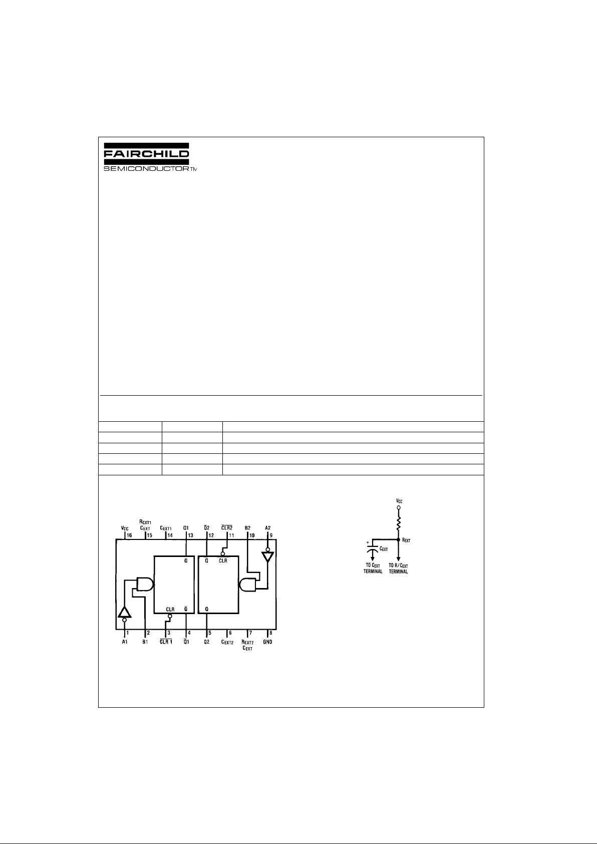
Connection Diagram
Pin Assignment for DIP, SOIC, SOP and TSSOP
Top View
Timing Component
Note: Pin 6 and Pin 14 must be ha rd-wired to GND.
Order Number Package Number Package Description
MM74HC123AM M16A 16-Lead Small Outline Integrated Circuit (SOIC), JEDEC MS-012, 0.150” Narrow
MM74HC123ASJ M16D 16-Lead Small Outline Package (SOP), EIAJ TYPE II, 5.3mm Wide
MM74HC123AMTC MTC16 16-Lead Thin Shrink Small Outline Package (TSSOP), JEDEC MO-153, 4.4mm Wide
MM74HC123AN N16E 16-Lead Plastic Dual-In-Line Package (PDIP), JEDEC MS-001, 0.300” Wide
Page 2
www.fairchildsemi.com 2
MM74HC123A
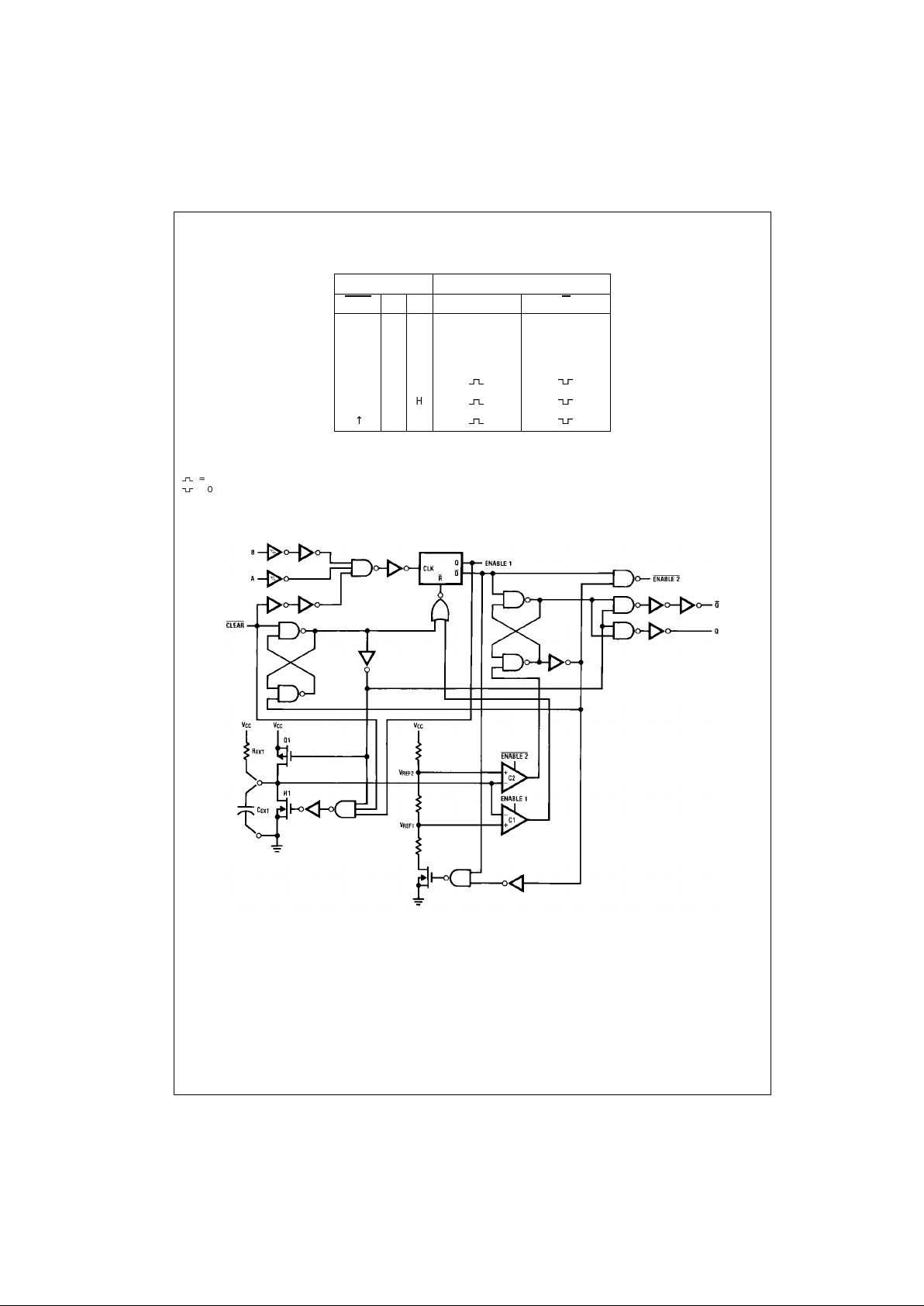
Truth Table
H = HIGH Level
L = LOW Level
↑=Transition from LOW-to-HIGH
↓=Transition from HIGH-to-LOW
= One HIGH Level Pulse
= One LOW Level Pulse
X = Irrelevant
Logic Diagram
Inputs Outputs
Clear
AB Q Q
LXX L H
XHX L H
XXL L H
HL↑
H ↓ H
↑ LH
Page 3
3 www.fairchildsemi.com
MM74HC123A
Absolute Maximum Ratings(Note 1)
(Note 2)
Recommended Operating
Conditions
Note 1: Maximum Ratings are those values beyond which damage to the
device may occur.
Note 2: Unless otherwise specified all voltages are referenced to ground.
Note 3: Power Dissipation Temperature Derating: Plast ic “N” Package: −
12mW/°C from 65°C to 85°C
DC Electrical Characteristics (Note 4)
Note 4: For a power supply of 5V ±10% the worst-case output voltages (VOH, VOL) occur for HC at 4.5V. Thus the 4.5V values should be us ed w hen design-
ing with this supply. Worst-case V
IH
and VIL occur at V
CC
= 5.5V and 4.5V resp ec t iv ely. (The VIH value at 5.5V is 3.85V.) The worst-cas e leakage current
(I
IN
, ICC, and IOZ) occur for CMOS at the higher voltage and s o t he 6.0V values should be used.
Supply Voltage (VCC) −0.5V to +7.0V
DC Input Voltage (V
IN
) −1.5V to V
CC
+1.5V
DC Output Voltage (V
OUT
) −0.5V to V
CC
+0.5V
Clamp Diode Current (I
IK
, IOK) ±20 mA
DC Output Current, per pin (I
OUT
) ±25 mA
DC V
CC
or GND Current, per pin (ICC) ±50 mA
Storage Temperature Range (T
STG
) −65°C to +150°C
Power Dissipation (P
D
)
(Note 3) 600 mW
S.O. Package only 500 mW
Lead Temperature (T
L
)
(Solderi ng 10 seconds) 260°C
Min Max Units
Supply Voltage (V
CC
)26V
DC Input or Output Voltage 0 V
CC
V
(V
IN
, V
OUT
)
Operating Temperature Range (T
A
) −40 +85 °C
Input Rise or Fall Times
(Clear Input)
(t
r
, tf)V
CC
= 2.0V 1000 ns
V
CC
= 4.5V 500 ns
V
CC
= 6.0V 400 ns
Symbol Parameter Conditions
V
CC
TA = 25°CTA = −40 to 85°CTA = −55 to 125°C
Units
Typ Guaranteed Limits
V
IH
Minimum HIGH Level Input 2.0V 1.5 1.5 1.5 V
Voltage 4.5V 3.15 3.15 3.15 V
6.0V 4.2 4.2 4.2 V
V
IL
Maximum LOW Level Input 2.0V 0.3 0.3 0.3 V
Voltage 4.5V 0.9 0.9 0.9 V
6.0V 1.2 1.2 1.2 V
V
OH
Minimum HIGH Level V
IN
= VIH or V
IL
Output Voltage |I
OUT
| ≤ 20 µA 2.0V 2.0 1.9 1.9 1.9 V
4.5V 4.5 4.4 4.4 4.4 V
6.0V 6.0 5.9 5.9 5.9 V
V
IN
= VIH or V
IL
V
|I
OUT
| ≤ 4.0 mA 4.5V 4.2 3.98 3.84 3.7 V
|I
OUT
| ≤ 5.2 mA 6.0V 5.7 5.48 5.34 5.2 V
V
OL
Maximum LOW Level V
IN
= VIH or V
IL
Output Voltage |I
OUT
| ≤ 20 µA 2.0V 0 0.1 0.1 0.1 V
4.5V 0 0.1 0.1 0.1 V
6.0V 0 0.1 0.1 0.1 V
V
IN
= VIH or V
IL
V
|I
OUT
| ≤ 4 mA 4.5V 0.2 0.26 0.33 0.4 V
|I
OUT
| ≤ 5.2 mA 6.0V 0.2 0.26 0.33 0.4 V
I
IN
Maximum Input Current V
IN
= VCC or GND 6.0V ±0.5 ±5.0 ±5.0 µA
(Pins 7, 15)
I
IN
Maximum Input Current V
IN
= VCC or GND 6.0V ±0.1 ±1.0 ±1.0 µA
(all other pins)
I
CC
Maximum Quiescent Supply V
IN
= VCC or GND 6.0V 8.0 80 160 µA
Current (standby) I
OUT
= 0 µA
I
CC
Maximum Active Supply VIN= VCC or GND 2.0V 36 80 110 130 µA
Current (per R/C
EXT
= 0.5V
CC
4.5V 0.33 1.0 1.3 1.6 mA
monostable) 6.0V 0.7 2.0 2.6 3.2 mA
Page 4

www.fairchildsemi.com 4
MM74HC123A
AC Electrical Characteristics
V
CC
= 5V, TA = 25°C, CL = 15 pF, tr = t
f
= 6 ns
AC Electrical Characteristics
C
L
= 50 pF tr = t
f
= 6 ns (unless otherwise specified)
Note 5: CPD determines the no lo ad dynamic power con s um ption, PD = CPD VCC2 f + ICC VCC, and the no load dynam ic c urrent consumption,
I
S
= CPD VCC f + ICC.
Symbol Parameter Conditions Typ Limit Units
t
PLH
Maximum Trigger Propagation Delay 22 33 ns
A, B or Clear to Q
t
PHL
Maximum Trigger Propagation Delay 25 42 ns
A, B or Clear to Q
t
PHL
Maximum Propagation Delay, Clear to Q 20 27 ns
t
PLH
Maximum Propagation Delay, Clear to Q
22 33 ns
t
W
Minimum Pulse Width, A, B or Clear 14 26 ns
t
REM
Minimum Clear Removal Time 0ns
t
WQ(MIN)
Minimum Output Pulse Width C
EXT
= 28 pF 400 ns
R
EXT
= 2 kΩ
t
WQ
Output Pulse Width C
EXT
= 1000 pF 10 µs
R
EXT
= 10 kΩ
Symbol Parameter Conditions
V
CC
TA = 25°CTA = −40 to 85°CTA = −55 to 125°C
Units
Typ Guaranteed Limits
t
PLH
Maximum Trigger Propagation 2.0V 77 169 194 210 ns
Delay, A, B or Clear to Q 4.5V 26 42 51 57 ns
6.0V 21 32 39 44 ns
t
PHL
Maximum Trigger Propagation 2.0V 88 197 229 250 ns
Delay, A, B or Clear to Q
4.5V 29 48 60 67 ns
6.0V 24 38 46 51 ns
t
PHL
Maximum Propagation Delay 2.0V 54 114 132 143 ns
Clear to Q 4.5V 23 34 41 45 ns
6.0V 19 28 33 36 ns
t
PLH
Maximum Propagation Delay 2.0V 56 116 135 147 ns
Clear to Q
4.5V 25 36 42 46 ns
6.0V 20 29 34 37 ns
t
W
Minimum P ulse Width 2.0V 57 123 144 157 ns
A, B, Clear 4.5V 17 30 37 42 ns
6.0V 12 21 27 30 ns
t
REM
Minimum Clear 2.0V 0 0 0 ns
Removal Time 4.5V 0 0 0 ns
6.0V 0 0 0 ns
t
TLH
, t
THL
Maximum Output 2.0V 30 75 95 110 ns
Rise and Fall Time 4.5V 8 15 19 22 ns
6.0V 7 13 16 19 ns
t
WQ(MIN)
Minimum Output C
EXT
= 28 pF 2.0V 1.5 µs
Pulse Width R
EXT
= 2 kΩ 4.5V 450 ns
R
EXT
= 6 kΩ (V
CC
= 2V) 6.0V 380 ns
t
WQ
Output Pulse Width C
EXT
= 0.1 µF Min 5.0V 1 0.9 0.86 0.85 ms
R
EXT
= 10 kΩ Max 5.0V 1 1.1 1.14 1.15 ms
C
IN
Maximum Input 12 20 20 20 p F
Capacitance (Pins 7 & 15)
C
IN
Maximum Input 6 10 10 10 pF
Capacitance (other inputs)
C
PD
Power Dissipation (Note 5) 70 pF
Capacitance
Page 5

5 www.fairchildsemi.com
MM74HC123A
Theory of Operation
1POSITIVE EDGE TRIGGER
2NEGATIVE EDGE TRIGGER
3POSITIVE EDGE TRIGGER
4POSITIVE EDGE RE-TRIGGER (PULSE LENGTHENING)
5RESET PULSE SHORTENING
6CLEAR TRIGGER
FIGURE 1.
TRIGGER OPERATION
As shown in
Figure 1
and the logic diagr am, before an
input trigger occurs, the one shot is in the quiescent state
with the Q output LOW, and the timing capacitor C
EXT
com-
pletely charged to V
CC
. When the trigger input A goes from
V
CC
to GND (while inputs B and clear are held to VCC) a
valid trigger is recognized, which turns on comparator C1
and Nchannel transistor N11. At the same time the output
latch is set. With transistor N1 on, the ca pacitor C
EXT
rap-
idly discharges toward GND until V
REF1
is reached. At this
point the output o f c ompar ator C 1 c hanges state an d tra nsistor N1 turns off. Comparator C1 then turns off while at
the same time comparat or C2 turns on . With tr ansistor N1
off, the capacitor C
EXT
begins to charge through the timing
resistor, R
EXT
, toward VCC. When the voltage across C
EXT
equals V
REF2
, comparator C2 change s state causing the
output latch to reset (Q goe s LOW) wh ile at the sa me time
disabling comparator C2. T his ends the timing cycle with
the monostable in the quiescent state, waiting for the next
trigger.
A valid trigger is also recognized when trigger input B goes
from GND to V
CC
(while input A is at GND and input clear
is at V
CC
2). The MM74HC123A can also be triggered when
clear goes from GND to V
CC
(while A is at GND and B is at
V
CC
6).
It should be noted that in the quiescent s tate C
EXT
is fully
charged to V
CC
causing the current thro ugh resistor R
EXT
to be zero. Both comparators are “off” with the total device
current due only to reverse junction leakages . An added
feature of the MM74HC12 3A is that the ou tput latch is set
via the input trigger without regar d to the cap acito r voltage.
Thus, propagation delay from trigger to Q is independent of
the value of C
EXT
, R
EXT
, or the duty cycle of the input
waveform.
RETRIGGER OPERATION
The MM74HC123A is re trig gered if a valid tr igge r occurs 3
followed by another trigger 4 before the Q output has
returned to the qu iescent (zero) state. Any retrigger, after
the timing node voltage at the R/C
EXT
pin has begun to rise
from V
REF1
, but has not yet reached V
REF2
, will cause an
increase in output pulse width T. When a valid retrigger is
initiated 4, the voltage at the R/C
EXT
pin will again drop to
V
REF1
before progressing along the RC charging curve
toward V
CC
. The Q output will remain HIGH u ntil time T,
after the last valid retrigger.
Because the trigger-control circuit flip-flop resets shortly
after C
X
has discharged to the reference voltage of the
lower reference c ircuit, the m inimum retri gger time, t
rr
is a
function of internal prop agation delays and the discharge
time of C
X
:
Another removal/ret rigger time occurs when a short clear
pulse is used. Upon receipt of a clear, the one shot must
charge the capacitor up to the upper tr ip point before the
one shot is ready to r eceive the next trigger. This time is
dependent on the capacitor used and is approximately:
Page 6

www.fairchildsemi.com 6
MM74HC123A
RESET OPERATI ON
These one shots may be reset du ri ng the ge ne rat ion of the
output pulse. In the reset mode of operation, an input pulse
on clear sets the reset latch and causes the capacitor to be
fast charged to V
CC
by turning on transistor Q1 5. When
the voltage on the capac it or r eac hes V
REF2
, the reset latch
will clear and then be ready to accept another pulse. If the
clear input is held low, any trigger inputs that occur will be
inhibited and the Q and Q
outputs of the output latch will
not change. Since the Q output is reset when an inpu t low level is detected on the Clear input, th e output pu lse T can
be made significantly shorter than the minimum pulse width
specification.
Typical Output Pulse
Width vs. Timing Components
Typical Distribution of Output
Pulse Width, Part to Part
Typical 1ms Pulse Width
Variation vs. Supply
Minimum R
EXT
vs.
Supply Voltage
Typical 1ms Pulse Width
Variation vs. Temperature
Note: R and C are not subjected to temperature. The C is polypropylene.
Page 7

7 www.fairchildsemi.com
MM74HC123A
Physical Dimensions inches (millimeters) unless otherwise noted
16-Lead Small Outline Integrated Circuit (SOIC), JEDEC MS-012, 0.150” Narrow
Package Number M16A
16-Lead Small Outline Package (SOP), EIAJ TYPE II, 5.3mm Wide
Package Number M16D
Page 8

www.fairchildsemi.com 8
MM74HC123A
Physical Dimensions inches (millimeters) unless otherwise noted (Continued)
16-Lead Thin Shrink Small Outline Package (TSSOP), JEDEC MO-153, 4.4mm Wide
Package Number MTC16
Page 9

Fairchild does not assume any responsibility for use of any circuitry described, no circuit patent licenses are implied and Fairchild reserves the right at any time without notice to change said circuitry and specifications.
MM74HC123A Dual Retriggerable Monostable Multivibrator
LIFE SUPPORT POLICY
FAIRCHILD’S PRODUCTS ARE NOT AUTHORIZED FOR USE AS CRITICAL COMPONENTS IN LIFE SUPPORT
DEVICES OR SYSTEMS WITHOUT THE EXPRESS WRITTEN APPROVAL OF THE PRESIDENT OF FAIRCHILD
SEMICONDUCTOR CORPORATION. As used herein:
1. Life support devices or systems are devices or systems
which, (a) are intended for surgical implant into the
body, or (b) support or sustain life, and (c) whose failure
to perform when properly used in accordance with
instructions for use provided i n the labe li ng, can be re asonably expected to result in a significant injury to the
user.
2. A critical component in any componen t of a life s uppor t
device or system whose failu re to perform can b e reasonably expected to c ause th e fa i lure of the li fe s upp or t
device or system, or to affect its safety or effectiveness.
www.fairchildsemi.com
Physical Dimensions inches (millimeters) unless otherwise noted (Continued)
16-Lead Plastic Dual-In-Line Package (PDIP), JEDEC MS-001, 0.300” Wide
Package Number N16E
 Loading...