

Page 1
查询MM74C90供应商
MM74C90 • MM74C93
4-Bit Decade Counter • 4-Bit Binary Counter
MM74C90 • MM74C93 4-Bit Decade Counter • 4-Bit Binary Counter
October 1987
Revised January 1999
General Description
The MM74C90 decad e counter and the M M74C93 binar y
counter and comple mentary MOS (CMO S) integrated circuits constructed with N- and P-channel enhancement
mode transistors. The 4-bit decade counter can reset to
zero or preset to nine by applying appropriate logic level on
, R02, R91 and R92 inputs. Also, a separate flip-flop
the R
01
on the A-bit enables the user to op erat e it as a di vide -by-2,
5 or 10 frequency counter. The 4-bit bina r y counte r can be
reset to zero by applying h igh logic level on inputs R
, and a separate flip-f lop on the A- bit enables the user
R
02
01
to operate it as a divide-by-2, -8, or -16 divider. Counting
occurs on the negative going edge of the input pulse.
All inputs are protected against static discharge damage.
Features
■ Wide supply voltage range: 3V to 15V
■ Guaranteed noise margin: 1V
■ High noise immunity: 0.45 V
■ Low power compatibility:
and
Fan out of 2 TTL driving 74L
■ The MM74C93 follows the MM74L93 Pinout
CC
(typ.)
Ordering Code:
Order Number Package Number Package Description
MM74C90N N14A 14-Lead Plastic Dual-In-Line Package (PDIP), JEDEC MS-001, 0.300” Wide
MM74C93N N14A 14-Lead Plastic Dual-In-Line Package (PDIP), JEDEC MS-001, 0.300” Wide
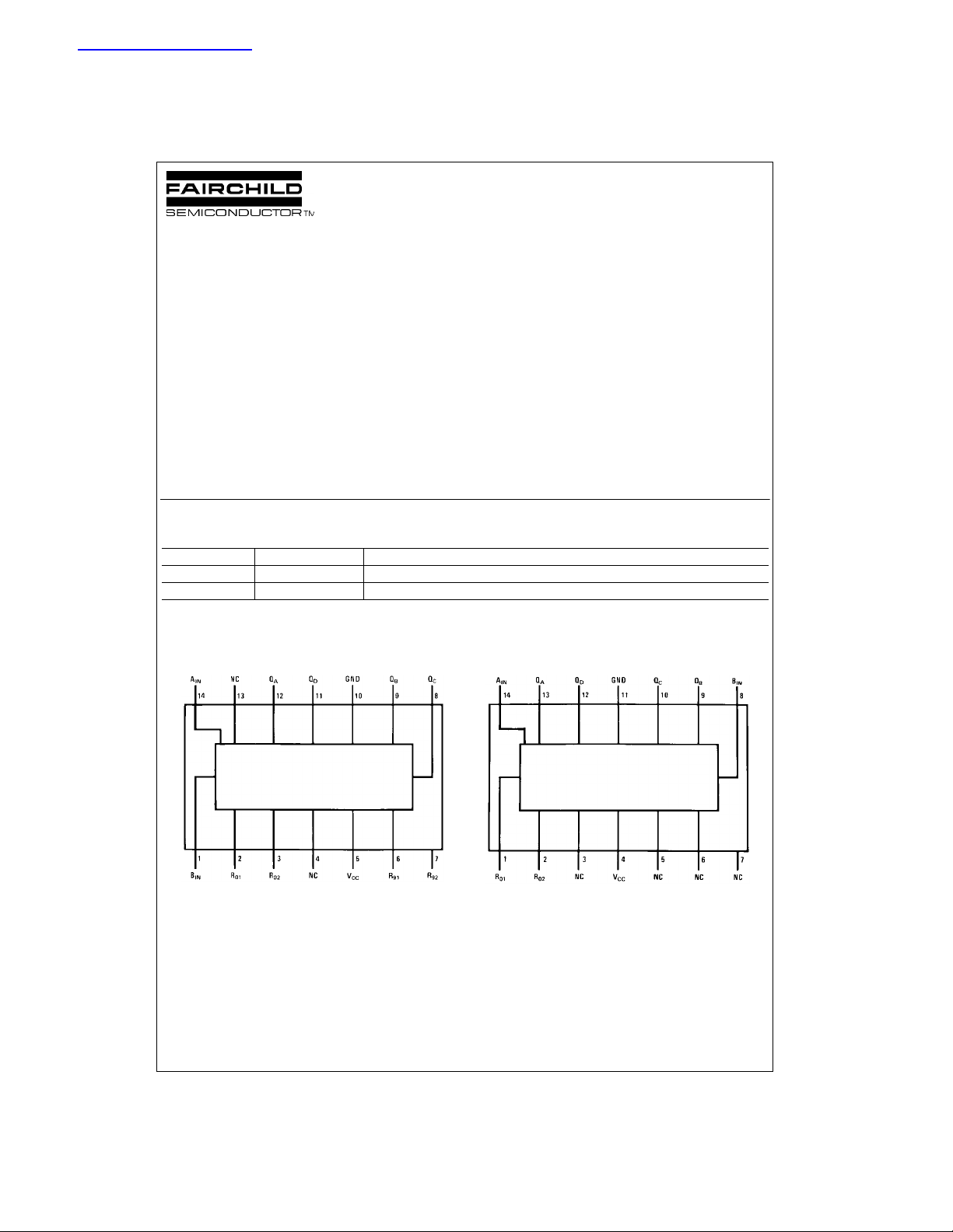
Connection Diagrams
Pin Assignments for DIP
MM74C90
MM74C93
Top View
© 1999 Fairchild Semiconductor Corporation DS005889.prf www.fairchildsemi.com
Top V iew
Page 2

Logic Diagrams
MM74C90 • MM74C93
Truth Tables
MM74C90 MM74C93
MM74C90 4-Bit Decade Counter BCD Count Sequence
Count Output
Q
DQCQBQA
0LLLL
1LLLH
2LLHL
3LLHH
4LHLL
5LHLH
6LHHL
7LHHH
8HLLL
9HLLH
Output QA is connected to Input B for BCD count.
H = HIGH Level
L = LOW Level
X = Irrelevant
MM74C93 4-Bit Binary Counter Binary Count Sequence
Count Output
Q
DQCQBQA
0 LLLL
1LLLH
2LLHL
3LLHH
4LHLL
5LHLH
6LHHL
7 LHHH
8 HLLL
9HLLH
10 H L H L
11 H L H H
12 H H L L
13 H H L H
14 H H H L
15 HHHH
Output QA is connected to input B for binary count sequence.
H = HIGH Level
L = LOW Level
X = Irrelevant
www.fairchildsemi.com 2
Page 3
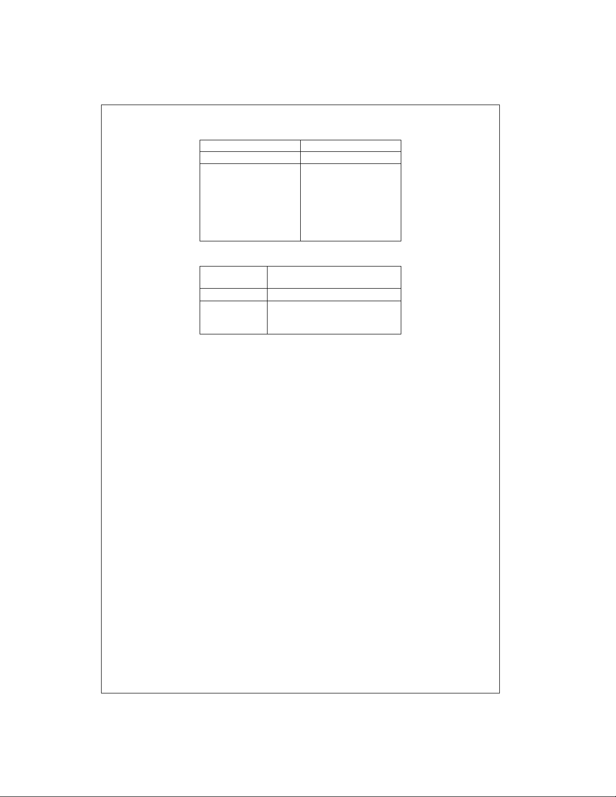
Function Tables
Reset/Count Function Table
Reset Inputs Output
R
01R02R91R92
QDQ
C
QBQ
A
HHLXLLLL
HHXLLLLL
XXHHHLLH
X L X L Count
LXLX Count
L X X L Count
X L L X Count
Reset/Count Function Table
Reset Output
Inputs
R
R
01
Q
02
Q
D
Q
C
Q
B
A
HHLLLL
L X Count
X L Count
MM74C90 • MM74C93
3 www.fairchildsemi.com
Page 4

Absolute Maximum Ratings(Note 1)
Voltage at Any Pin (Note 1) −0.3V to VCC +0.3V
Operating Temperature Range (T
MM74C90, MM74C93 −40°C to +85°C
Power Dissipation (P
)
D
Dual-In-Line 700 mW
Small Outline 500 mW
Operating V
Range 3V to 15V
CC
)
A
Absolute Maximum V
Storage Temperature Range (T
Lead Temperature (T
CC
)
L
) −65°C to +150°C
S
(Soldering, 10 seconds) 260°C
Note 1: “Absolute Maxi mum Ratings” are those valu es beyond which the
safety of the device cannot be guaranteed. Exce pt for “O perating Temperature Range”, they are not mean t to imply that the device s should be operated at these limits. The table of “Electrical Characteristics” provides
conditions for actual device op eration.
MM74C90 • MM74C93
DC Electrical Characteristics
Min/Max limits apply across temperature range unless otherwise noted
Symbol Parameter Conditions Min Typ Max Units
CMOS TO CMOS
V
IN(1)
V
IN(0)
V
OUT(1)
V
OUT(0)
I
IN(1)
I
IN(0)
I
CC
CMOS/LPTTL INTERFA CE
V
IN(1)
V
IN(0)
V
OUT(1)
V
OUT(0)
OUTPUT DRIVE (See Family Characteristics Data Sheet) (Short Circuit Current)
I
SOURCE
I
SOURCE
I
SINK
I
SINK
Logical “1” Input Voltage VCC = 5V 3.5 V
Logical “0” Input Voltage VCC = 5V 1.5 V
Logical “1” Output Voltage VCC = 5V, IO = −10 µA4.5 V
Logical “0” Output Voltage VCC = 5V, IO = +10 µA0.5V
Logical “1” Input Current VCC = 15V, VIN = 15V 0.005 1.0 µA
Logical “0” Input Current VCC = 15V, VIN = 0V −1.0 −0.005 µA
Supply Current VCC = 15V 0.05 300 µA
Logical “1” Input Voltage
MM74C90, MM74C93 VCC = 4.75V VCC−1.5 V
Logical “0” Input Voltage
MM74C90, MM74C93 VCC = 4.75V 0.8 V
Logical “1” Output Voltage
MM74C90, MM74C93 VCC = 4.75V, IO = −360 µA2.4 V
Logical “0” Output Voltage
MM74C90, MM74C93 VCC = 4.75V, IO = −360 µA0.4V
Output Source Current VCC = 5V, V
(P-Channel) TA = 25°C
Output Source Current VCC = 10V, V
(P-Channel) TA = 25°C
Output Sink Current VCC = 5V, V
(N-Channel) TA = 25°C
Output Sink Current VCC = 10V, V
(N-Channel) TA = 25°C
VCC = 10V 8.0 V
VCC = 10V 2.0 V
VCC = 10V, IO = −10 µA9.0 V
VCC = 10V, IO = +10 µA1.0V
= 0V −1.75 −3.3 mA
OUT
= 0V −8.0 −15 mA
OUT
OUT
OUT
= V
= V
CC
CC
1.75 3.6 mA
8.0 16 mA
18V
www.fairchildsemi.com 4
Page 5

AC Electrical Characteristics (Note 2)
= 25°C, CL = 50 pF, unless otherwise specified
T
A
Symbol Parameter Conditions Min Typ Max Units
t
, t
pd0
t
pd0
t
pd0
t
pd0
t
pd0
t
pd0
t
pd0
t
pd0
t
pd0
t
pd0
t
PW
t
PW
t
PW
tr, t
t
W
f
MAX
C
C
Note 2: AC Parameters are guaranteed by DC correlated testin g.
Note 3: Capacitance is guaranteed by periodic testing.
Note 4: C
AN-90.
Propagation Delay Time VCC = 5V 200 400 ns
pd1
from AIN to Q
, t
Propagation Delay Time from VCC = 5V 450 850 ns
pd1
A
VCC = 10 80 150 ns
AIN to QB (MM74C93) VCC = 10V 160 300 ns
, t
Propagation Delay Time from VCC = 5V 450 800 ns
pd1
AIN to QB (MM74C90) VCC = 10V 160 300 ns
, t
Propagation Delay Time VCC = 5V 500 1050 ns
pd1
from AIN to QC (MM74C93) VCC = 10 200 400 ns
, t
Propagation Delay Time from VCC = 5V 500 1000 ns
pd1
AIN to QC (MM74C93) VCC = 10V 200 400 ns
, t
Propagation Delay Time from VCC = 5V 600 1200 ns
pd1
AIN to QD (MM74C93) VCC = 10V 250 500 ns
, t
Propagation Delay Time from VCC = 5V 450 800 ns
pd1
AIN to QD (MM74C90) VCC = 10V 160 300 ns
, t
Propagation Delay Time from VCC = 5V 150 300 ns
pd1
R01 or R02 to QA, QB, QC or Q
D
VCC = 10V 75 150 ns
(MM74C93)
, t
Propagation Delay Time from VCC = 5V 200 400 ns
pd1
R01 or R02 to QA, QB, QC or Q
D
VCC = 10V 75 150 ns
(MM74C90)
, t
Propagation Delay Time from VCC = 5V 250 500 ns
pd1
R91 or R92 to QA or Q
D
VCC = 10V 100 200 ns
(MM74C90)
Min. R01 or R02 Pulse Width VCC = 5V 600 250 ns
(MM74C93) VCC = 10V 30 125 ns
Min. R01 or R02 Pulse Width VCC = 5V 600 250 ns
(MM74C90) VCC = 10V 300 125 ns
Min. R91 or R92 Pulse Width VCC = 5V 500 200 ns
(MM74C90) VCC = 10V 250 100 ns
Maximum Clock Rise VCC = 10V 15 µs
f
and Fall Time VCC = 10V 5 µs
Minimum Clock Pulse Width VCC = 5V 250 100 ns
VCC = 10V 100 50 ns
Maximum Clock Frequency VCC = 5V 2 MHz
VCC = 10V 5 MHz
Input Capacitance Any Input (Note 3) 5 pF
IN
Power Dissipation Capacitance Per Package (Note 4) 45 pF
PD
determines t he no l oad a c power c onsump tion of any CM OS device. For comp lete explan ation s ee Family Ch aracte ristics applic ation note —
PD
MM74C90 • MM74C93
5 www.fairchildsemi.com
Page 6

AC Test Circuits
MM74C90 • MM74C93
MM74C90
MM74C93
Clock rise and fall time tr = tf = 20 ns
Switching Time Waveforms
Clock rise and fall time tr = tf = 20 ns
MM74C90 and M M 74C93 are solid line waveforms. Dashed line waveforms are for MM74C90 only.
www.fairchildsemi.com 6
Page 7

Physical Dimensions inches (millimeters) unless otherwise noted
MM74C90 • MM74C93 4-Bit Decade Counter • 4-Bit Binary Counter
14-Lead Plastic Dual-In-Line Package (PDIP), JEDEC MS-001, 0.300” Wide
LIFE SUPPORT POLICY
FAIRCHILD’S PRODUCTS ARE NOT AUTHORIZED FOR USE AS CRITICAL COMPONENTS IN LIFE SUPPORT
DEVICES OR SYSTEMS WITHOUT THE EXPRESS WRITTEN APPROVAL OF THE PRESIDENT OF FAIRCHILD
SEMICONDUCTOR CORPORATION. As used herein:
1. Life supp ort devices or systems are devices or syste ms
which, (a) are intended for surgical implant into the
body, or (b) support or sustain life, and (c) whose failure
to perform when properly used in accordance with
instructions for use provided in the label in g, can be re asonably expected to result i n a significant injur y to the
user.
Package Number N14A
2. A critic al com ponen t in any com ponen t of a l ife support
device or system whose failure to perform can be reasonably expected to cause the failure of the life support
device or system, or to affect its safety or effectiveness.
www.fairchildsemi.com
Fairchild does not assume any responsibility for use of any circuitry described, no circuit patent licenses are implied and Fairchil d reser ves the right at any time without notice to change said circuitry and specifications.
 Loading...