

Page 1
查询74C925供应商
MM74C925 • MM74C926 • MM74C927 • MM74C928
4-Digit Counters with Multiplexed
7-Segment Output Drivers
MM74C925 • MM74C926 • MM74C927 • MM74C928 4-Digit Counters with Multiplexed 7-Segment Output Drivers
October 1987
Revised January 1999
General Description
The MM74C925, MM74C 9 26, M M74 C92 7 and MM7 4C 9 28
CMOS counters consist of a 4-digit counter, an internal output latch, NPN output sourcing drivers for a 7-segment display, and an internal multiplexing circuitry with four
multiplexing outputs. The multiplexing circuit has its own
free-running oscillator, and requires no external clock. The
counters advance on negative edge of clock. A HIGH signal on the Reset input will reset the counter to zero, and
reset the carry-out LOW. A LOW signal on the Latch
Enable input will latch the number in the counters into the
internal output latches. A HIGH signal on Disp lay Select
input will select the number in the coun ter to be displ ayed;
a LOW level signal on the Display Select will select the
number in the output latch to be displayed.
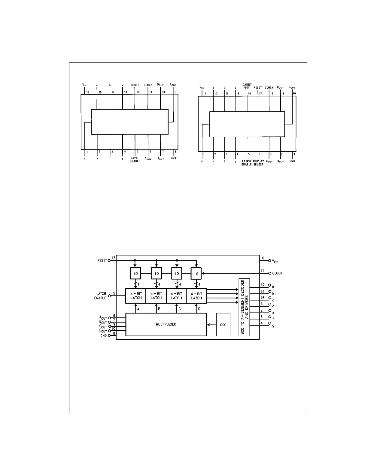
The MM74C925 is a 4-decade counter and has Latch
Enable, Clock and Reset inputs.
The MM74C926 is like the MM74C9 25 except that it ha s a
display select and a carry-out used for cascading counters.
The carry-out sig nal goes HIGH at 6000 , goes back LOW
at 0000.
The MM74C927 is like the M M74C926 except the second
most significant digi t divides by 6 rather than 10. Thu s, if
the clock input frequency is 10 Hz, the display would read
tenths of seconds and minutes (i.e., 9:59.9).
The MM74C928 is like the MM74C926 except the most significant digit divides by 2 rather than 10 and the carry-out is
an overflow indicator which is HIGH at 2000, and it goes
Ordering Code:
back LOW only when the count er is reset. Thus, thi s is a
3½-digit counter.
Features
■ Wide supply voltage range: 3V to 6V
■ Guaranteed noise margin: 1V
■ High noise immunity: 0.45 V
■ High segment sourcing current: 40 mA
− 1.6V, VCC = 5V
@ V
CC
■ Internal multiplexing circuitry
CC
(typ.)
Design Considerations
Segment resistors are desirable to minimize po wer dissipation and chip heating. The D S754 92 se rves as a good digit
driver when it is desired to drive bright displays. When
using this driver w it h a 5V su pp ly a t r oom tem pera tur e, the
display can be driven without segment resistors to full illumination. The user must use cautio n in thi s mo de however,
to prevent overheating of the d evice by using too high a
supply voltage or by operati ng at high ambient temperatures.
The input protection circ uitry consists of a series resist or,
and a diode to gro und. Thus input signals exceeding V
will not be clamped. This input signal should not be allowed
to exceed 15V .
CC
Order Number Package Number Package Description
MM74C925N N16E 16-Lead Plastic Dual-In-Line Package (PDIP), JEDEC MS-001, 0.300” Wide
MM74C926N N18A 18-Lead Plastic Dual-In-Line Package (PDIP), JEDEC MS-001, 0.300” Wide
MM74C927N N18A 18-Lead Plastic Dual-In-Line Package (PDIP), JEDEC MS-001, 0.300” Wide
MM74C928N N18A 18-Lead Plastic Dual-In-Line Package (PDIP), JEDEC MS-001, 0.300” Wide
© 1999 Fairchild Semiconductor Corporation DS005919.prf www.fairchildsemi.com
Page 2
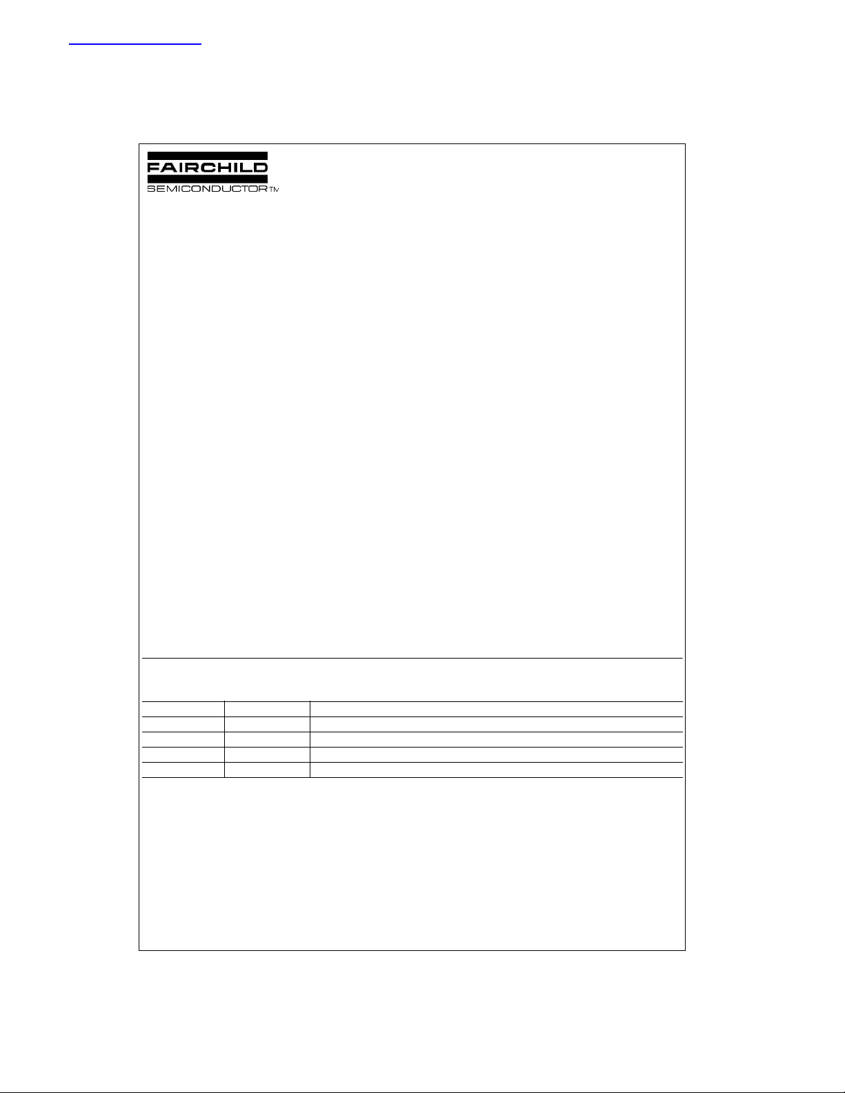
Connection Diagrams
Pin Assignments for DIP
Top View
MM74C925
Functional Description
Reset — Asynchronous, active high
Display Select — High, displays output of counter
Low, displays output of latch
Latch Enable — High, flow through condition
MM74C925 • MM74C926 • MM74C927 • MM74C928
Clock —Negative edge sensitive
Low, latch condition
Logic Diagrams
MM74C926, MM74C927, MM74C928
Segment Output — Current sourcing with 40 mA @V
Digit Output — Current sourcing with 1 mA @V
Carry-Out — 2 LTTL loads. See carry-out waveforms.
MM74C925
V
CC
LTTL loads
1.75V. Also, sink capability = 2 LTTL loads
Top View
− 1.6V (typ.) Also, sink capability = 2
OUT
OUT
=
=
www.fairchildsemi.com 2
Page 3
Logic Diagrams (Continued)
MM74C925 • MM74C926 • MM74C927 • MM74C928
MM74C926
MM74C927
MM74C928
3 www.fairchildsemi.com
Page 4

Absolute Maximum Ratings(Note 1)
Voltage at Any Output Pin GND − 0.3V to VCC + 0.3V
Voltage at Any Input Pin GND − 0.3V to +15V
Operatin g Temperature
Range (T
Storage Temperature
Range −65°C to +150°C
Power Dissipation (P
) −40°C to +85°C
A
)Refer to P
D
D(MAX)
vs TA Graph
Operating V
V
CC
Lead Temperature
(Soldering, 10 seconds) 260°C
Note 1: “Absolute Maxi mum Ratings” are those valu es beyond which the
safety of the device cannot be guaranteed. Ex ce pt for “O perating Temperature Range” they are not mean t to imply that the devices sho uld be operated at these limits. The Electrical Charac t eristics table provide s co nditions
for actual device operation.
Range 3V to 6V
CC
DC Electrical Characteristics
Min/Max limits apply at −40°C ≤ tj≤ + 85°C, unless otherwise noted
Symbol Parameter Conditions Min Typ Max Units
CMOS TO CMOS
V
IN(1)
V
IN(0)
V
OUT(1)
V
OUT(0)
I
IN(1)
I
IN(0)
I
CC
MM74C925 • MM74C926 • MM74C927 • MM74C928
CMOS/LPTTL INTERFA CE
V
IN(1)
V
IN(0)
V
OUT(1)
V
OUT(0)
OUTPUT DRIVE
V
OUT
R
ON
I
I
SOURCE
I
SINK
θ
jA
Note 2: θjA measured in free-air w it h device soldered into print ed circuit board.
Logical “1” Input Voltage VCC = 5V 3.5 V
Logical “0” Input Voltage VCC = 5V 1.5 V
Logical “1” Output Voltage VCC = 5V, IO = −10 µA
(Carry-Out and Digit Output 4.5 V
Only)
Logical “0” Output Voltage VCC = 5V, IO = 10 µA0.5V
Logical “1” Input Current VCC = 5V, VIN = 15V 0.005 1 µA
Logical “0” Input Current VCC = 5V, VIN = 0V −1 −0.005 µA
Supply Current VCC = 5V, Outputs Open Circuit, 20 1000 µA
VIN = 0V or 5V
Logical “1” Input Voltage VCC = 4.75V VCC − 2V
Logical “0” Input Voltage VCC = 4.75V 0.8 V
Logical “1” Output Voltage VCC = 4.75V,
(Carry-Out and Digit IO = −360 µA2.4 V
Output Only)
Logical “0” Output Voltage VCC = 4.75V, IO = 360 µA0.4V
Output Voltage (Segment I
Sourcing Output) I
= −65 mA, VCC = 5V, Tj = 25°CVCC − 2VCC − 1.3 V
OUT
= −40 mA, VCC = 5V Tj = 100°CVCC − 1.6 VCC − 1.2 V
OUT
Tj = 150°CVCC − 2VCC − 1.4 V
Output Resistance (Segment I
Sourcing Output) I
= −65 mA, VCC = 5V, Tj = 25°C2032Ω
OUT
= −40 mA, VCC = 5V Tj = 100°C3040Ω
OUT
Tj = 150°C3550Ω
Output Resistance (Segment 0.6 0.8 %/°C
Output) Temperature Coefficient
Output Source Current VCC = 4.75V, V
SOURCE
= 1.75V, Tj = 150°C −1 −2mA
OUT
(Digit Output)
Output Source Current VCC = 5V, V
= 0V, Tj = 25°C −1.75 −3.3 mA
OUT
(Carry-Out)
Output Sink Current VCC = 5V, V
= VCC, Tj = 25°C 1.75 3.6 mA
OUT
(All Outputs)
Thermal Resistance MM74C925: (Note 2) 75 100 °C/W
MM74C926, MM74C927, MM74C928 70 90 °C/W
6.5V
www.fairchildsemi.com 4
Page 5

AC Electrical Characteristics (Note 3)
= 25°C, CL = 50 pF, unless otherwise noted
T
A
Symbol Parameter Conditions Min Typ Max Units
f
MAX
tr, t
t
WR
t
WLE
t
SET(CK, LE)
t
LR
t
SET(R, LE)
f
MUX
C
IN
Note 3: AC Parameters are guaranteed by DC correlated testing.
Note 4: Capacitance is guaranteed by periodic testing.
Maximum Clock Frequency VCC = 5V, Tj = 25°C24 MHz
Maximum Clock Rise or Fall Time VCC = 5V 15 µs
f
Reset Pulse Width VCC = 5V Tj = 25°C 250 100 ns
Latch Enable Pulse Width VCC = 5V Tj = 25°C 250 100 ns
Clock to Latch Enable Set-Up Time VCC = 5V Tj = 25°C 2500 1250 ns
Latch Enable to Reset Wait Time VCC = 5V Tj = 25°C0−100 ns
Reset to Latch Enable Set-Up Time VCC = 5V Tj = 25°C 320 160 ns
Multiplexing Output Frequency VCC = 5V 1000 Hz
Input Capacitance Any Input (Note 4) 5 pF
Squar e Wave Clock Tj = 100°C1.53 MHz
Tj = 100°C 320 125 ns
Tj = 100°C 320 125 ns
Tj = 100°C 3200 1600 ns
Tj = 100°C0−100 ns
Tj = 100°C 400 200 ns
Typical Performance Characteristics
MM74C925 • MM74C926 • MM74C927 • MM74C928
Typical Segment Current
vs Output Voltage
Note: VD = Voltage across digit driver
Maximum Power Dissipation
vs Ambient Temperature
Typical Average Segment
Current vs Segment
Resistor Value
5 www.fairchildsemi.com
Page 6

Typical Performance Characteristics (Continued)
Segment Output Driver Input Protection
Common Cathode LED Display
MM74C925 • MM74C926 • MM74C927 • MM74C928
Segment Identification
www.fairchildsemi.com 6
Page 7

Switching Time Waveforms
Input Waveforms Multiplexing Output Waveforms
T = 1/f
MUX
Carry-Out Waveforms
MM74C925 • MM74C926 • MM74C927 • MM74C928
7 www.fairchildsemi.com
Page 8

Physical Dimensions in ches (millimeters) unless otherwise noted
MM74C925 • MM74C926 • MM74C927 • MM74C928
16-Lead Plastic Dual-In-Line Package (PDIP), JEDEC MS-001, 0.300” Wide
Package Number N16E
www.fairchildsemi.com 8
Page 9

Physical Dimensions inches (millimeters) unless otherwise noted (Continued)
MM74C925 • MM74C926 • MM74C927 • MM74C928 4-Digit Counters with Multiplexed 7-Segment Output Drivers
18-Lead Plastic Dual-In-Line Package (PDIP), JEDEC MS-001, 0.300” Wide
LIFE SUPPORT POLICY
FAIRCHILD’S PRODUCTS ARE NOT AUTHORIZED FOR USE AS CRITICAL COMPONENTS IN LIFE SUPPORT
DEVICES OR SYSTEMS WITHOUT THE EXPRESS WRITTEN APPROVAL OF THE PRESIDENT OF FAIRCHILD
SEMICONDUCTOR CORPORATION. As used herein:
1. Life support devices or system s a re devices or syste ms
which, (a) are intended for surgical implant into the
body, or (b) support or sustain life, and (c) whose failure
to perform when properly used in accordance with
instructions for use provided in the labeling, can be reasonably expected to result in a significant injur y to the
user.
Package Number N18A
2. A critical comp onent in any com ponent of a l ife support
device or system whose failure to perform can be reasonably expected to cause the failure of the life suppor t
device or system, or to affect its safety or effectiveness.
www.fairchildsemi.com
Fairchild does not assume any responsibility for use of any circuitry described, no circui t patent licenses are implied and Fairchild reserves the right at any time without notice to change said circuitry and specifications.
 Loading...