

Datasheet MM74C923WMX, MM74C923N, MM74C923CW, MM74C923WM Datasheet (Fairchild Semiconductor)
Page 1
October 1987
Revised January 1999
MM74C922 • MM74C923 16-Key Encoder • 20-Key Encoder
© 1999 Fairchild Semiconductor Corporation DS006037.prf www.fairchildsemi.com
MM74C922 • MM74C923
16-Key Encoder • 20-Key Encoder
General Description
The MM74C922 and MM74C923 CMOS key encoders provide all the necessary logic to fully encode an array of
SPST switches. The keyboard scan can be imp lemented
by either an external clock or external capacitor. These
encoders also have on-chip pull-up devices which pe rmit
switches with up to 50 kΩ on resistance to be used. No
diodes in the switch array are needed to eliminate ghost
switches. The internal debounce circuit needs only a single
external capacitor and can be defeated by omitting the
capacitor. A Data Available output goes to a high level
when a valid keyboard entry has been m ade. The Data
Available output returns to a low level when the entered
key is released, even if another key is depressed. The Data
Available will return high to indicate acceptan ce of the new
key after a normal debou nce period; this t wo-key roll-over
is provided between any two switches.
An internal regist er remembers the last key pressed even
after the key is released. The 3 -STATE outputs provide for
easy expansion and bus operation and are LPTTL compatible.
Features
■ 50 kΩ maximum switch on resistance
■ On or off chip clock
■ On-chip row pull-up devices
■ 2 key roll-over
■ Keybounce elimination with single capacitor
■ Last key register at outputs
■ 3-STATE output LPTTL compatible
■ Wide supply range: 3V to 15V
■ Low power consumption
Ordering Code:
Device also available in Tape and Reel. Specify by appendin g s uf f ix let t er “X” to the ordering co de.
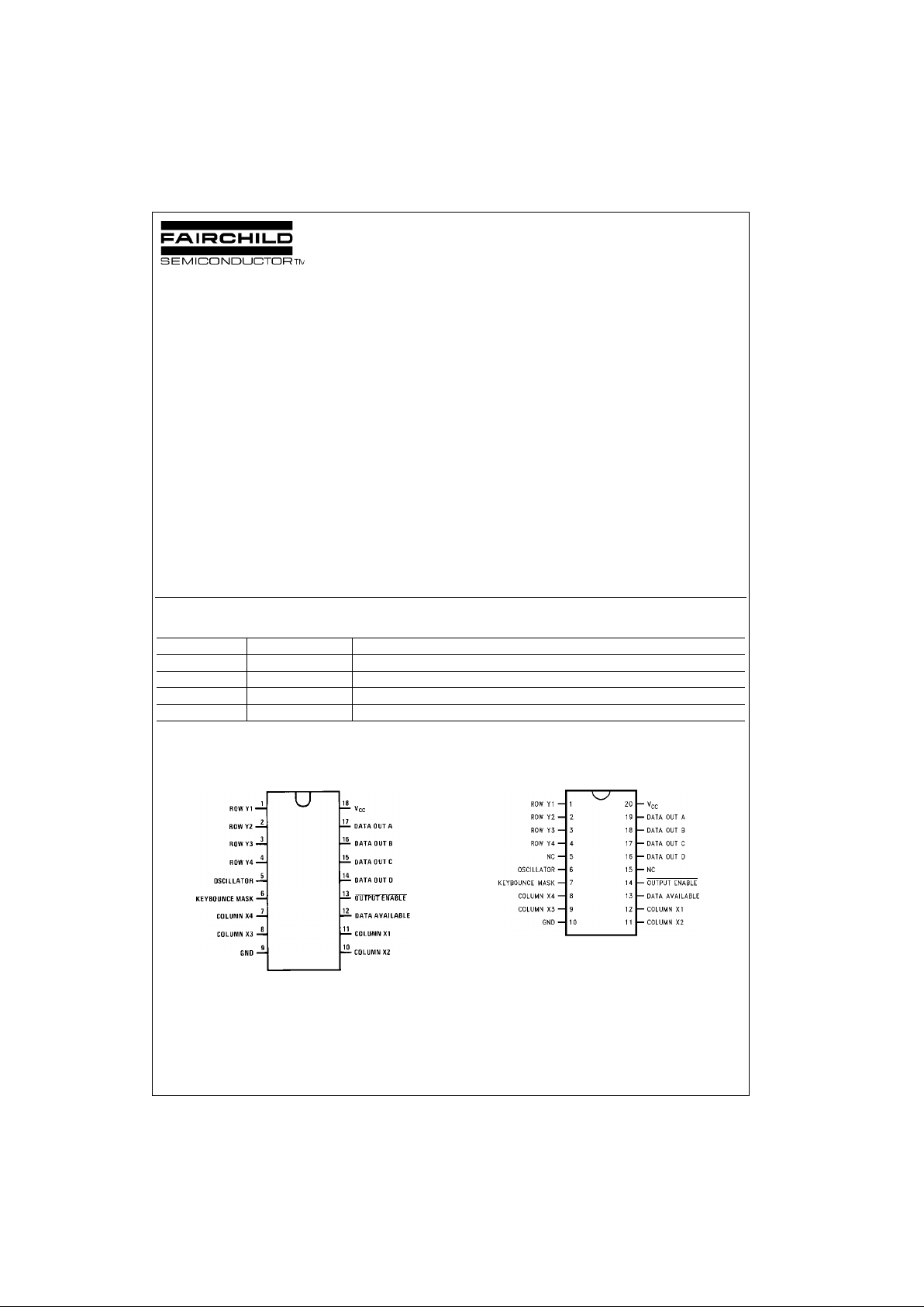
Connection Diagrams
Pin Assignment for DIP
Top View
MM94C922
Pin Assignment for SOIC
Top Vi ew
MM74C922
Order Number Package Number Package Description
MM74C922N N18A 18-Lead Plastic Dual-In-Line Package (PDIP), JEDEC MS-001, 0.300” Wide
MM74C922WM M20B 20-Lead Small Outline Integrated Circuit (SOIC), JEDEC MS-013, 0.300” Wide
MM74C923WM M20B 20-Lead Small Outline Integrated Circuit (SOIC), JEDEC MS-013, 0.300” Wide
MM74C923N N20A 20-Lead Plastic Dual-In-Line Package (PDIP), JEDEC MS-001, 0.300” Wide
Page 2

www.fairchildsemi.com 2
MM74C922 • MM74C923
Connection Diagrams (Continued)
Pin Assignment f or
DIP and SOIC Package
Top View
MM74C923
Truth Tables
(Pins 0 through 11)
(Pins 12 through 19)
Note 1: Omit for MM74C 922
Switch
Position
01234 5678910 11
Y1,X1 Y1,X2 Y1,X3 Y1,X4 Y2,X1 Y2,X2 Y2,X3 Y2,X4 Y3,X1 Y3,X2 Y3,X3 Y3,X4
D
AA 010101010101
TB 001100110011
AC 000011110000
OD 000000001111
UE
(Note 1)000000000000
T
Switch
Position
12 13 14 15 16 17 18 19
Y4,X1 Y4,X2 Y4,X3 Y4,X4 Y5(Note 1),X1Y5 (Note 1),X2Y5 (Note 1),X3 Y5 (Note 1),
X4
D
AA 0101 0 1 0 1
TB 0011 0 0 1 1
AC 1111 0 0 0 0
OD 1111 0 0 0 0
UE
(Note 1) 0 0 0 0 1 1 1 1
T
Page 3

3 www.fairchildsemi.com
MM74C922 • MM74C923
Block Diagram
Page 4

www.fairchildsemi.com 4
MM74C922 • MM74C923
Absolute Maximum Ratings(Note 2)
Note 2: “Absolute Maxi mum Ratings” are those valu es beyond which the
safety of the device cannot be guaranteed. Ex ce pt for “O perating Temperature Range” they are not mean t to imply that the devices sho uld be operated at these limits. The table of “Electrical Characteristics” provides
conditions for actual device op eration.
DC Electrical Characteristics
Min/Max limits apply across temperature range unless otherwise specified
Voltage at Any Pin VCC − 0.3V to V
CC
+ 0.3V
Operating Temperature Range
MM74C922, MM74C923 −40°C to +85°C
Storage Temperature Range −65°C to +150°C
Power Dissipation (P
D
)
Dual-In-Line 700 mW
Small Outline 500 mW
Operating V
CC
Range 3V to 15V
V
CC
18V
Lead Temperature
(Soldering, 10 seconds) 260°C
Symbol Parameter Conditions Min Typ Max Units
CMOS TO CMOS
V
T+
Positive-Going Threshold Voltage VCC = 5V, IIN ≥ 0.7 mA 3.0 3.6 4.3 V
at Osc and KBM Inputs VCC = 10V, IIN ≥ 1.4 mA 6.0 6.8 8.6 V
VCC = 15V, IIN ≥ 2.1 mA 9.0 10 12.9 V
V
T−
Negative-Going Threshold Voltage VCC = 5V, IIN ≥ 0.7 mA 0.7 1.4 2.0 V
at Osc and KBM Inputs VCC = 10V, IIN ≥ 1.4 mA 1.4 3.2 4.0 V
VCC = 15V, IIN ≥ 2.1 mA 2.1 5 6.0 V
V
IN(1)
Logical “1” Input Voltage, VCC = 5V 3.5 4.5 V
Except Osc and KBM Inputs VCC = 10V 8.0 9 V
VCC = 15V 12.5 13.5 V
V
IN(0)
Logical “0” Input Voltage, VCC = 5V 0.5 1.5 V
Except Osc and KBM Inputs VCC = 10V 1 2 V
VCC = 15V 1.5 2.5 V
I
rp
Row Pull-Up Current at Y1, Y2, VCC = 5V, VIN = 0.1 V
CC
−2 −5 µA
Y3, Y4 and Y5 Inputs VCC = 10V −10 −20 µA
VCC = 15V −22 −45 µA
V
OUT(1)
Logical “1” Output Voltage VCC = 5V, IO = −10 µA4.5 V
VCC = 10V, IO = −10 µA9 V
VCC = 15V, IO = −10 µA13.5 V
V
OUT(0)
Logical “0” Output Voltage VCC = 5V, IO = 10 µA0.5V
VCC = 10V, IO = 10 µA 1V
VCC = 15V, IO = 10 µA 1.5V
R
on
Column “ON” Resistance at VCC = 5V, VO = 0.5V 500 1400 Ω
X1, X2, X3 and X4 Outputs VCC = 10V, VO = 1V 300 700 Ω
VCC = 15V, VO = 1.5V 200 500 Ω
I
CC
Supply Current VCC = 5V 0.55 1.1 mA
Osc at 0V, (one Y low) VCC = 10V 1.1 1.9 mA
VCC = 15V 1.7 2.6 mA
I
IN(1)
Logical “1” Input Current VCC = 15V, VIN = 15V 0.005 1.0 µA
at Output Enable
I
IN(0)
Logical “0” Input Current VCC = 15V, VIN = 0V −1.0 −0.005 µA
at Output Enable
CMOS/LPTTL INTERFA CE
V
IN(1)
Except Osc and KBM Inputs VCC = 4.75V VCC − 1.5 V
V
IN(0)
Except Osc and KBM Inputs VCC = 4.75V 0.8 V
V
OUT(1)
Logical “1” Output Voltage IO = −360 µA
VCC = 4.75V 2.4 V
IO = −360 µA
V
OUT(0)
Logical “0” Output Voltage IO = −360 µA
VCC = 4.75V 0.4 V
IO = −360 µA
Page 5

5 www.fairchildsemi.com
MM74C922 • MM74C923
DC Electrical Characteristics (Continued)
AC Electrical Characteristics (Note 3)
T
A
= 25°C, CL = 50 pF, unless otherwise noted
Note 3: AC Parameters are guaranteed by DC correlated testing.
Note 4: Capacitance is guaranteed by periodic testing.
Symbol Parameter Conditions Min Typ Max Units
OUTPUT DRIVE (See Family Characteristics Data Sheet) (Short Circuit Current)
I
SOURCE
Output Source Current VCC = 5V, V
OUT
= 0V, −1.75 −3.3 mA
(P-Channel) TA = 25°C
I
SOURCE
Output Source Current VCC = 10V, V
OUT
= 0V, −8 −15 mA
(P-Channel) TA = 25°C
I
SINK
Output Sink Current VCC = 5V, V
OUT
= VCC, 1.75 3.6 mA
(N-Channel) TA = 25°C
I
SINK
Output Sink Current VCC = 10V, V
OUT
= VCC, 816 mA
(N-Channel) TA = 25°C
Symbol Parameter Conditions Min Typ Max Units
t
pd0
, t
pd1
Propagation Delay Time to CL = 50 pF (Figure 1)
Logical “0” or Logical “1” VCC = 5V 60 150 ns
from D.A. VCC = 10V 35 80 ns
VCC = 15V 25 60 ns
t0H, t
1H
Propagation Delay Time from RL = 10k, CL = 10 pF (Figure 2)
Logical “0” or Logical “1” VCC = 5V, RL = 10k 80 200 ns
into High Impedance State VCC = 10V, C L = 10 pF 65 150 ns
VCC = 15V 50 110 ns
tH0, t
H1
Propagation Delay Time from RL = 10k, CL = 50 pF (Figure 2)
High Impedance State to a VCC = 5V, RL = 10k 100 250 ns
Logical “0” or Logical “1” VCC = 10V, CL = 50 pF 55 125 ns
VCC = 15V 40 90 ns
C
IN
Input Capacitance Any Input (Note 4) 5 7.5 pF
C
OUT
3-STATE Output Capacitance Any Output (Note 4) 10 pF
Page 6

www.fairchildsemi.com 6
MM74C922 • MM74C923
Switching Time Waveforms
T1 ≈ T2 ≈ RC, T3 ≈ 0.7 RC, where R ≈ 10k and C is external capacitor at KBM input.
FIGURE 1.
FIGURE 2.
Page 7

7 www.fairchildsemi.com
MM74C922 • MM74C923
Typical Performance Characteristics
Typical I
rp
vs VIN at Any Y Input T ypical Ron vs V
OUT
at Any X Output
Typical F
SCAN
vs C
OSC
Typical Debounce Period vs C
KBM
Typical Applications
Synchronous Handshake (MM74C9 22)
The keyboard may be synchronously scanned by omit ting the capacitor at
osc. and driving osc. directly if the system clock rate is lower than 10 kHz
Synchronous Data Entry Onto Bus (MM74C922)
Outputs are en abled wh en valid entr y is made and go in to 3-S TATE when
key is released.
The keyboard may be synchronously scanned by omitting the capacitor at
osc. and driving osc. directly if the system clock rate is lower than 10 kHz
Page 8

www.fairchildsemi.com 8
MM74C922 • MM74C923
Asynchronous Data Entry Ont o Bus (MM7 4C922)
Outputs are in 3-STATE until key is pressed, then data is placed on bus. When key is released, outputs return to 3-STATE.
Expansion to 3 2 Key Encoder (M M74C922)
Theory of Operation
The MM74C922/MM74C923 Keyboard Encoders implement all the logic necessary to interface a 16 or 20 SPST
key switch matrix to a digital system. The encoder will convert a key switch closer to a 4(MM74C922) or
5(MM74C923) bit nibble. The designer can control both the
keyboard scan rate and the key debounce per iod by altering the oscillator capacitor, C
OSE
, and the key bounce
mask capacitor, C
MSK
. Thus, the MM74C922/MM74 C 92 3’s
performance can be optimized for many keyboards.
The keyboard encoders connect to a switch matrix that is 4
rows by 4 columns (MM74C922) or 5 rows by 4 columns
(MM74C923). When no keys are depressed, the row inputs
are pulled high by internal pull-ups and the column outputs
sequentially output a logic “0”. These outputs are open
drain and are therefore low for 25% of the time and otherwise off. The column s can rate is co ntrolled by the oscilla tor input, which consists of a Schmitt trigger oscillator, a 2bit counter, and a 2–4-bit decoder.
When a key is depressed, key 0, for example, nothing will
happen when the X1 input is off, since Y1 will remain high.
When the X1 column is scanned, X1 goes low and Y1 will
go low. This disables the counter and keeps X1 low. Y1
going low also initiates th e key bounce circuit timing and
locks out the other Y inputs. The key code to be output is a
combination of the frozen counter value and the decoded Y
inputs. Once the key bounce circ uit times out, the data is
latched, and the Data Available (DAV) output goes high.
If, during the key closure the switch bounces, Y1 input will
go high again, restar ting the scan and resetting the key
bounce circuitry. The key may bounce several times, but as
soon as the switch stays low for a debounce peri od, the
closure is assumed valid and the data is latched.
A key may also bounce when it is released. To ensure that
the encoder doe s no t re cog ni z e th i s bo un c e as an ot h er k ey
closure, the debounce circuit mu st t ime ou t before an other
closure is recognized.
The two-key roll-over feature can be illustrated by assuming a key is depressed, and then a second key is
depressed. Since all scanning has stopped, and all other Y
inputs are disabled, the second key is no t recognized until
the first key is lifted and the key bounce circuitry has reset.
The output latche s feed 3-STATE, which is enabled when
the Output Enable (OE
) input is taken low.
Page 9

9 www.fairchildsemi.com
MM74C922 • MM74C923
Physical Dimensions inches (millimeters) unless otherwise noted
18-Lead Plastic Dual-In-Line Package (PDIP), JEDEC MS-001, 0.300” Wide
Package Number N18A
20-Lead Plastic Small Outline I.C. Package (M)
Package Number M20B
Page 10

Fairchild does not assume any responsibility for use of any circuitry descri bed, no circuit patent licenses are implied and Fairchild reser ves the right at any time without notice to change said circuitr y and specifications.
MM74C922 • MM74C923 16-Key Encoder • 20-Key Encoder
LIFE SUPPORT POLICY
FAIRCHILD’S PRODUCTS ARE NOT AUTHORIZED FOR USE AS CRITICAL COMPONENTS IN LIFE SUPPORT
DEVICES OR SYSTEMS WITHOUT THE EXPRESS WRITTEN APPROVAL OF THE PRESIDENT OF FAIRCHILD
SEMICONDUCTOR CORPORATION. As used herein:
1. Life support devices or systems ar e devices or syste ms
which, (a) are intended for surgical implant into the
body, or (b) support or sustain life, and (c) whose failure
to perform when properly used in accordance with
instructions for use provided in the labeling, can be reasonably expected to result in a significant injury to the
user.
2. A critical component in any comp onent of a li fe suppor t
device or system whose failure to perform can be reasonably expected to cause the failure of the life suppor t
device or system, or to affect its safety or effectiveness.
www.fairchildsemi.com
Physical Dimensions inches (millimeters) unless otherwise noted (Continued)
20-Lead Plastic Dual-In-Line Package (PDIP), JEDEC MS-001, 0.300” Wide
Package Number N20A
 Loading...