

Page 1
查询MM74C908供应商
MM74C908/MM74C918 Dual CMOS 30V Relay Driver
General Description
The MM74C908 and MM74C918 are general purpose dual
high voltage drivers, each capable of sourcing a minimum of
250 mA at V
The MM74C908 and MM74C918 consist of two CMOS
NAND gates driving an emitter follower Darlington output to
achieve high current drive and high voltage capabilities. In
the ‘‘OFF’’ state the outputs can withstand a maximum of
b
30V across the device. These CMOS drivers are useful in
interfacing normal CMOS voltage levels to driving relays,
regulators, lamps, etc.
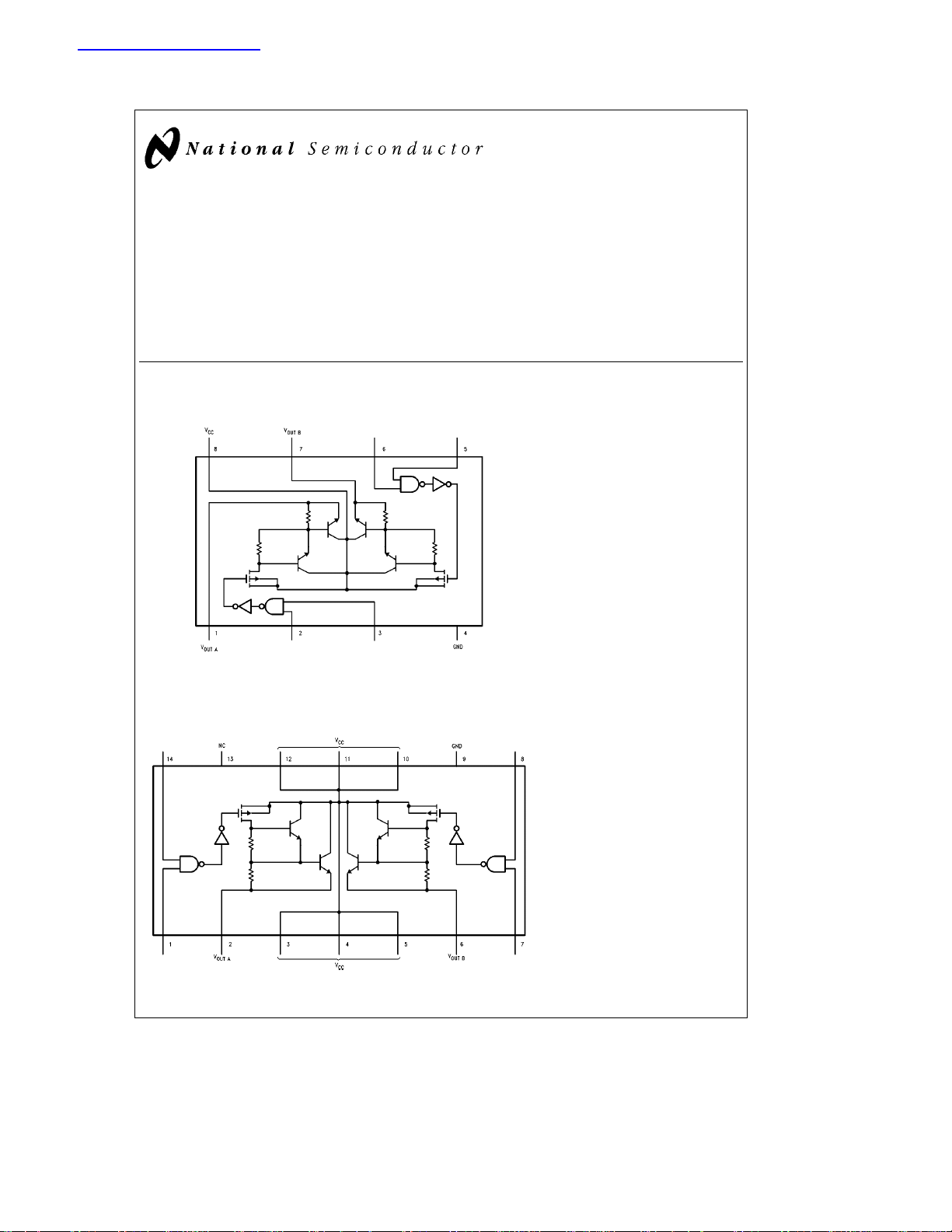
Connection Diagrams
OUT
e
V
b
3V, and T
CC
Dual-In-Line Package
MM74C908
MM74C908/MM74C918 Dual CMOS 30V Relay Driver
November 1990
Features
Y
Wide supply voltage range 3V to 18V
Y
e
65§C.
J
High noise immunity 0.45 VCC(typ.)
Y
Low output ‘‘ON’’ resistance 8X (typ.)
Y
High voltage
Y
High current 250 mA
b
30V
Order Number MM74C908
Top View
TL/F/5912– 1
Dual-In-Line Package
MM74C918
Order Number MM74C918
Top View
TL/F/5912– 2
TRI-STATEÉis a registered trademark of National Semiconductor Corporation.
C
1995 National Semiconductor Corporation RRD-B30M105/Printed in U. S. A.
TL/F/5912
Page 2
Absolute Maximum Ratings (Note 1)
If Military/Aerospace specified devices are required,
please contact the National Semiconductor Sales
Office/Distributors for availability and specifications.
Voltage at any Input Pin
b
0.3V to V
CC
a
0.3V
Voltage at any Output Pin 32V
Operating Temperature Range
MM74C908/MM74C918
b
40§Ctoa85§C
Operating V
Absolute Maximum V
I
SOURCE
Storage Temperature Range (TS)
Lead Temperature (TL)
(Soldering, 10 seconds) 260
Power Dissipation (PD) Refer to Maximum Power
Range 4V to 18V
CC
CC
b
65§Ctoa150§C
Dissipation vs Ambient
Temperature Graph
500 mA
DC Electrical Characteristics Min/Max limits apply across temperature range, unless otherwise noted
Symbol Parameter Conditions Min Typ Max Units
CMOS TO CMOS
V
V
I
IN(1)
I
IN(0)
I
CC
IN(1)
IN(0)
Logical ‘‘1’’ Input Voltage V
Logical ‘‘0’’ Input Voltage V
Logical ‘‘1’’ Input Current V
Logical ‘‘0’’ Input Current V
Supply Current V
Output ‘‘OFF’’ Voltage V
CMOS/LPTTL INTERFACE
V
V
IN(1)
IN(0)
Logical ‘‘1’’ Input Voltage
MM74C908/MM74C918 V
Logical ‘‘0’’ Input Voltage
MM74C908/MM74C918 V
OUTPUT DRIVE
V
R
i
OUT
ON
JA
Output Voltage I
Output Resistance I
Output Resistance 0.55 0.80 %/§C
Coefficient
Thermal Resistance (Note 3) 100 110§C/W
MM74C908/MM74C918 (Note 3) 45 55
e
5V 3.5 V
CC
e
10V 8.0 V
V
CC
e
5V 1.5 V
CC
e
10V 2.0 V
V
CC
OUT
I
OUT
I
OUT
OUT
I
OUT
I
OUT
CC
CC
CC
IN
CC
CC
e
e
e
e
e
e
eb
eb
eb
eb
eb
eb
VCC,I
e
15V, V
15V, V
15V 0.005 1.0 mA
IN
e
0V
IN
b
1.0
b
0.005 mA
15V, Outputs Open Circuit 0.05 15 mA
eb
OUT
200 mA
4.75V V
CC
b
b
30 V
1.5 V
4.75V 0.8 V
t
300 mA, V
250 mA, V
175 mA, V
300 mA, V
250 mA, V
175 mA, V
CC
CC
CC
CC
CC
CC
t
t
t
t
t
e
5V, T
25§CV
J
e
5V, T
65§CV
J
e
5V, T
150§CV
J
e
5V, T
25§C 6.0 9.0 X
J
e
5V, T
65§C 7.5 12 X
J
e
5V, T
150§C1018X
J
CC
CC
CC
b
2.7 V
b
3.0 V
b
3.15 V
b
1.8 V
CC
b
1.9 V
CC
b
2.0 V
CC
19V
C/W
§
C
§
AC Electrical Characteristics*
Symbol Parameter Conditions Min Typ Max Units
t
pd1
t
pd0
C
IN
*AC Parameters are guaranteed by DC correlated testing.
Note 1: ‘‘Absolute Maximum Ratings’’ are those values beyond which the safety of the device cannot be guaranteed. Except for ‘‘Operating Temperature Range’’
they are not meant to imply that the devices should be operated at these limits. The table of ‘‘Electrical Characteristics’’ provides conditions for actual device
operation.
Note 2: Capacitance is guaranteed by periodic testing.
Note 3: i
JA
Propagation Delay V
to a Logical ‘‘1’’ C
Propagation Delay V
to a Logic ‘‘0’’ C
Input Capacitance (Note 2) 5.0 pF
measured in free air with device soldered into printed circuit board.
e
CC
e
L
e
V
CC
e
C
L
e
CC
e
L
e
V
CC
e
C
L
5V, R
50 pF, T
10V, R
50 pF, T
5V, R
50 pF, T
10V, R
50 pF, T
e
50X,
L
e
25§C
A
e
50X,
L
e
25§C
A
e
50X,
L
e
25§C
A
e
50X,
L
e
25§C
A
150 300 ns
65 120 ns
2.0 10 ms
4.0 20 ms
2
Page 3

Typical Performance Characteristics
Maximum Power Dissipation
vs Ambient Temperature
AC Test Circuit
Typical I
vs Typical V
OUT
Maximum V
vs I
OUT
OUT
b
CC
V
OUT
Typical I
OUT
Typical I
Typical V
vs Typical V
OUT
Switching Time Waveforms
OUT
OUT
vs
TL/F/5912– 3
TL/F/5912– 4
e
e
t
t
20 ns
r
f
TL/F/5912– 5
3
Page 4

Power Considerations
Calculating Output ‘‘ON’’ Resistance (R
The output ‘‘ON’’ resistance, RON, is a function of the junction temperature, T
e
9(T
R
ON
, and is given by:
J
b
25) (0.008)a9 (1)
J
and TJis given by:
e
a
T
T
P
J
A
where T
ance, and P
device. P
leakage currents, internal capacitance, switching, etc.)
e
A
DAV
consists of normal CMOS power terms (due to
DAV
, (2)
DAViJA
ambient temperature, i
is the average power dissipated within the
which are insignificant when compared to the power dissipated in the outputs. Thus, the output power term defines
the allowable limits of operation and includes both outputs,
A and B. P
P
is given by:
D
2
e
I
OA
R
ON
D
2
a
I
RON, (3)
OB
where IOis the output current, given by:
b
V
V
CC
e
I
O
is the load voltage.
V
L
L
a
R
R
ON
L
The average power dissipation, P
duty cycle:
2
e
P
I
DAV
RON(Duty CycleA)
OA
2
I
RON(Duty CycleB)
OB
where the duty cycle is the % time in the current source
state. Substituting equations (1) and (5) into (2) yields:
e
T
T
J
[
simplifying:
T
A
e
T
J
1b0.072 i
a
i
A
2
I
(Duty CycleA)aI
OA
a
7.2 i
[
JA
[
I
JA
OA
[
I
JA
OA
b
9(T
25) (0.008)a9
J
2
(Duty CycleA)aI
2
(Duty CycleA)aI
OB
Equations (1), (4), and (6b) can be used in an iterative method to determine the output current, output resistance and
junction temperature.
l
18X)
L
e
thermal resist-
JA
, is a function of the
DAV
a
]
2
(Duty CycleB)
2
(Duty CycleB)
OB
2
(Duty CycleB)
OB
(4)
(5)
(6a)
]
]
]
For example, let V
e
V
0V, T
L
50%, Duty Cycle
Assuming R
I
OA
I
OB
A
ON
V
CC
e
R
ON
V
CC
e
R
ON
and
a
T
7.2 i
A
e
T
J
1b0.072 i
25a(7.2) (110)[(0.1351)2(0.5)a(0.1351)2(0.75)
e
T
J
1b(0.072) (110)[(0.1351)2(0.5)a(0.1351)2(0.75)
e
T
52.6§C
J
e
and R
9(T
ON
e
9(52.6b25) (0.008)a9e11X
CC
e
25§C, i
e
B
e
11X, then:
b
V
L
a
R
LA
b
V
L
a
R
LB
2
[
I
JA
OA
[
I
JA
OA
b
25) (0.008)a9
J
e
15V, R
e
JA
75%.
15
e
11a100
e
135.1 mA
(Duty CycleA)aI
2
(Duty CycleA)aI
e
100X,R
LA
110§C/W, Duty Cycle
e
135.1 mA,
2
(Duty CycleB)
OB
2
(Duty CycleB)
OB
TL/F/5912– 6
e
LB
]
]
]
]
100X,
A
e
Applications
(See AN-177 for applications)
4
Page 5

Physical Dimensions inches (millimeters)
Ceramic Dual-In-Line Package (J)
Order Number MM74C918J
NS Package Number J14A
Molded Dual-In-Line Package (N)
Order Number MM74C908N
NS Package Number N08E
5
Page 6
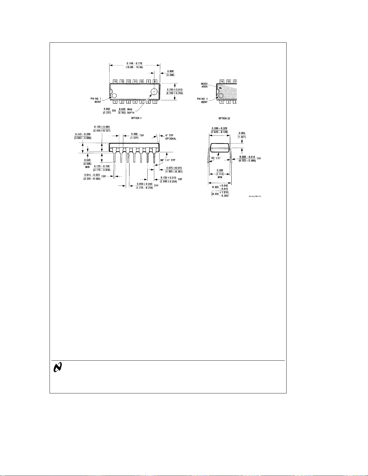
Physical Dimensions inches (millimeters) (Continued)
Molded Dual-In-Line Package (N)
Order Number MM74C918N
NS Package Number N14A
MM74C908/MM74C918 Dual CMOS 30V Relay Driver
LIFE SUPPORT POLICY
NATIONAL’S PRODUCTS ARE NOT AUTHORIZED FOR USE AS CRITICAL COMPONENTS IN LIFE SUPPORT
DEVICES OR SYSTEMS WITHOUT THE EXPRESS WRITTEN APPROVAL OF THE PRESIDENT OF NATIONAL
SEMICONDUCTOR CORPORATION. As used herein:
1. Life support devices or systems are devices or 2. A critical component is any component of a life
systems which, (a) are intended for surgical implant support device or system whose failure to perform can
into the body, or (b) support or sustain life, and whose be reasonably expected to cause the failure of the life
failure to perform, when properly used in accordance support device or system, or to affect its safety or
with instructions for use provided in the labeling, can effectiveness.
be reasonably expected to result in a significant injury
to the user.
National Semiconductor National Semiconductor National Semiconductor National Semiconductor
Corporation Europe Hong Kong Ltd. Japan Ltd.
1111 West Bardin Road Fax: (
Arlington, TX 76017 Email: cnjwge@tevm2.nsc.com Ocean Centre, 5 Canton Rd. Fax: 81-043-299-2408
Tel: 1(800) 272-9959 Deutsch Tel: (
Fax: 1(800) 737-7018 English Tel: (
National does not assume any responsibility for use of any circuitry described, no circuit patent licenses are implied and National reserves the right at any time without notice to change said circuitry and specifications.
Fran3ais Tel: (
Italiano Tel: (
a
49) 0-180-530 85 86 13th Floor, Straight Block, Tel: 81-043-299-2309
a
49) 0-180-530 85 85 Tsimshatsui, Kowloon
a
49) 0-180-532 78 32 Hong Kong
a
49) 0-180-532 93 58 Tel: (852) 2737-1600
a
49) 0-180-534 16 80 Fax: (852) 2736-9960
 Loading...