

Page 1
查询74C911供应商
MM74C911
4-Digit Expandable Segment Display Controller
MM74C911 4-Digit Expandable Segment Display Controller
October 1987
Revised January 1999
General Description
The MM74C911 display controll er is an interface element
with memory that drives a 4-digit, 8- segment LED d isplay.
The MM74C911 allows individual control of any segment in
the 4-digit display. The number of segments per digit can
be expanded without any exter nal c omponent s. For example, two MM74C911’s can be cascade d to drive a 16-se gment alpha-numeric display.
The display controllers receive data infor mation through 8
data lines a, b…DP, and digit information through 2
address inputs K1 and K2. The input data is written into the
register selected by the address information when CHIP
ENABLE, CE, a nd WRITE ENABLE, WE, are LOW and is
latched when either CE
is not required.
A self-contained internal oscillator sequentially presents
the stored data to hi g h d r ive (100 m A typ.) 3-STATE output
drivers which directly drive the LED display. The drivers are
active when the control pin labeled SEGMENT OUTPU T
ENABLE, SOE, is LOW and go into 3-STATE when SOE is
HIGH. This feature allows for duty cycle brightness control,
or for disabling the output drive for power conservation.
or WE return HIGH. Data hold time
The digit outputs di re ctly d r ive the ba se of the d igit t ransistor when the control p in labeled DIGIT INPUT OUTPUT
, is LOW. When DIO is HIGH, the digit lines turn into
DIO
inputs and the internal scanning multiplexer is disabled.
When any digit line is forced HIGH by an external device,
usually another MM74 C911, the data information for that
digit is presented to the output. In this manner, 16-segment
alpha-numeric dis plays, 24- or 32-segment d isplays, or an
array of discrete LED's can be controlled by the simple cascading of expandable segment display controllers. All
inputs except digit inpu ts are TTL compatible and do not
clamp input voltages above V
CC
.
Features
■ Direct segment drive (100 mA typ.) 3-STATE
■ 4 registers addressed like RAM
■ Internal oscillator and scanning circuit
■ Direct base drive to digit transistor
■ Segment expandability without external components
■ TTL compatible inputs
■ Power saver mode—5 µW (typ.)
Ordering Code:
Order Number Package Number Package Description
MM74C991N N28B 28-Lead Plastic Dual-In-Line Package (PDIP), JEDEC MS−010, 0.600” Wide
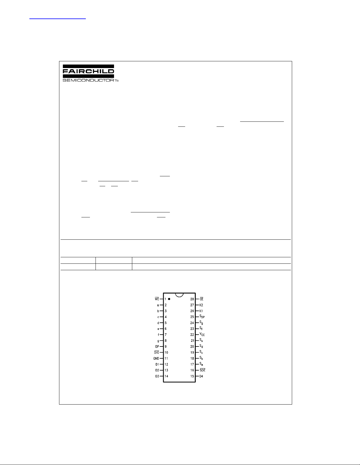
Connection Diagram
Pin Assignments for DIP
,
Top View
© 1999 Fairchild Semiconductor Corporation DS005915.prf www.fairchildsemi.com
Page 2
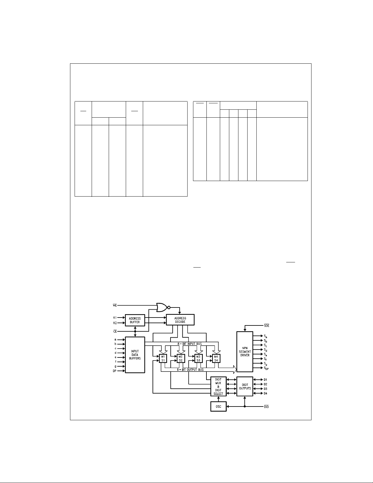
Truth Tables
MM74C911
CE
K2 K1
0 0 0 0 Write Digit 1
0 0 0 1 Latch Digit 1
0 0 1 0 Write Digit 2
0 0 1 1 Latch Digit 2
0 1 0 0 Write Digit 3
0 1 0 1 Latch Digit 3
0 1 1 0 Write Digit 4
0 1 1 1 Latch Digit 4
1 X X X Disable Writing
Input Control Output Control
Digit
Address WE Operation
Functional Description
The MM74C911 display controller is manufactured on standard metal gate CMOS techno logy. A single 5V 74 series
TTL supply can be used for power and should be bypassed
at the V
The digit outputs directly drive the base of a grounded
emitter digit transistor without the need of a Darlington configuration. If an MM74C911 is drivi ng a digit transistor and
also supplying digit information to a cascaded MM74C911,
base resistors are nee de d i n th e dig it transistors to provide
an adequate high level to the digit inputs of the cascaded
MM74C911.
As seen in the Block Diagram, these display controllers
contain four 8-bit regi sters; any one may be random ly wr it-
pin to suppress current transients.
CC
DIO SOE Digit Lines Operation
D4 D3 D2 D1
0 0 RRRRRefresh Display
0 1 RRRRDisable Segment Outputs
1 0 0000Digits Are Now Inputs
1 0 0001Display Digit 1
1 0 0010Display Digit 2
1 0 0100Display Digit 3
1 0 1000Display Digit 4
1 1 0000Power Saver Mode
R = Refresh (digit line s se quentially pulsed)
X = Don’t Care
ten into. In normal op eratio n, the i nte rnal multiplexer scans
the registers and refr esh es th e disp lay. In cascaded operation, 1 MM74C911 serves as a master refresh device and
cascaded MM74C911’s are slaved to it throu gh digit lines
operating as inputs.
The MM74C911 appea rs to a microprocessor a s memory
and to the user as a self-scan display. Since every segment is under microprocessor control, great versatility is
obtained.
Low power standby operation occurs w ith both SOE
inputs HIGH. This condition forces the MM74C911 to a
DIO
quiescent state typically drawing less than 1 µA of supply
current with a standby supply voltage as low as 3V.
and
Logic Diagram
www.fairchildsemi.com 2
Page 3
Absolute Maximum Ratings(Note 1)
(Note 2)
Voltage at Any Pin
except Inputs −0.3V to V
Voltage at Any Input
except Digits −0.3V to +15V
Operating Temperature
Range, (T
) −40°C to +85°C
A
Storage Temperature Range −65°C to +150°C
Power Dissipation (P
) Refer to P
D
D(MAX)
+ 0.3V
CC
vs TA Graph
Operating V
Absolute Maximum V
Lead Temperature
(Soldering, 10 seconds ) 260°C
Note 1: “Absolute Maximum Rat ings” are tho se values beyond which the
safety of the device cannot be guarant eed. Exce pt for “Operating Range”,
they are not meant to imply that the device should be operated at these limits. The table of “Electr ical Characteristic s” provides condition s for actual
device operation.
Note 2: All voltage reference to ground.
Range 3V to 6V
CC
CC
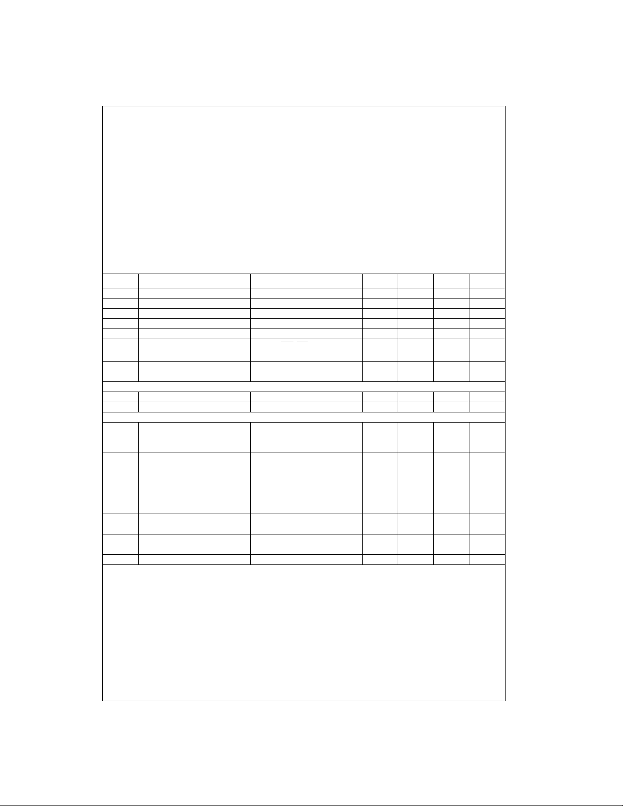
DC Electrical Characteristics
Min/Max limits apply at −40°C ≤ TJ ≤ +85°C, unless otherwise noted
Symbol Parameter Conditions Min Typ Max Units
V
IN(1)
V
IN(0)
I
IN(1)
I
IN(0)
I
CC
I
CC
I
OUT
CMOS/LPTTL INTERFACE
V
IN(1)
V
IN(0)
OUTPUT DRIVE
I
SH
I
DH
V
OUT(1)
V
OUT(0)
θ
JA
Note 3: θJA measured in free-air with device soldered into printed circuit board.
Logical “1” Input Voltage VCC = 5V 3.0 V
Logical “0” Input Voltage 1.5 V
Logical “1” Input Current VCC = 5V, VIN = 15V 0.005 1.0 µA
Logical “0” Input Current VCC = 5V, VIN = 0V −1.0 −0.005 µA
Supply Current (Normal) VCC = 5V, Outputs Open 0.50 2.5 mA
Supply Current (Power Saver)
3-STATE Output Current VO = 5V 0.03 10 µA
Logical “1” Input Voltage VCC = 4.75V VCC − 2V
Logical “0” Input Voltage VCC = 4.75V 0.8 V
HIGH Level Segment Current VCC = 5V, VO = 3.4V
HIGH Level Digit Current VCC = 5V, VO = 3V
Logical “1” Output Voltage, VCC = 5V, IO = −360 µA4.6 V
Any Digit
Logical “0” Output Voltage, VCC = 5V, IO = 360 µA0.4V
Any Output
Thermal Resistance (Note 3) 100 °C/W
VCC = 5V, SOE, DIO = “1”,
D1, D2, D3, D4 = “0”
VO = 0V −10 −0.03
TJ = 25°C −60 −100 mA
TJ = 100°C −40 −60 mA
TJ = 25°C −10 −20 mA
TJ = 100°C −7 −10 mA
VCC = 5V, VO = 1V
TJ = 25°C −15 −40 mA
TJ = 100°C −10 −15 mA
1 600 µA
MM74C911
6.5V
3 www.fairchildsemi.com
Page 4
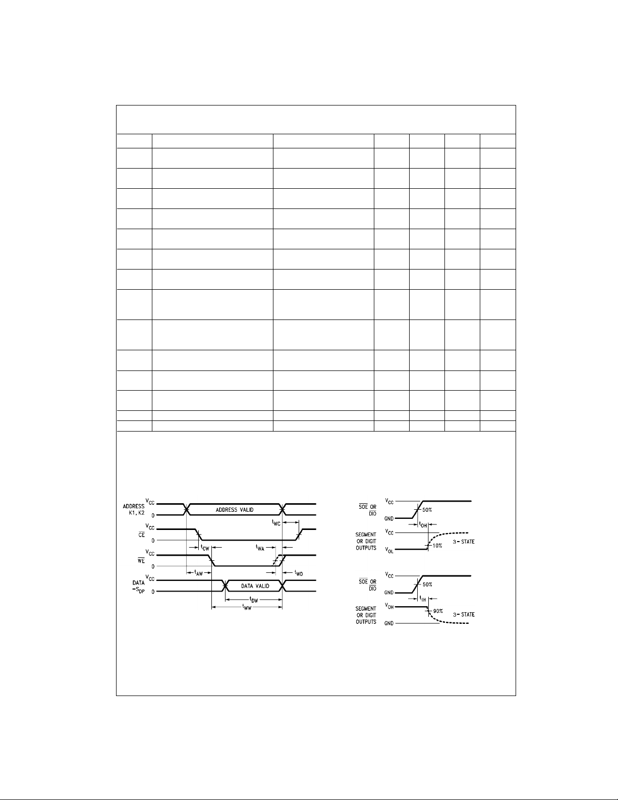
AC Electrical Charac teristics (Note 4)
VCC = 5V, tr = tf = 20 ns, CL = 50 pF
Symbol Parameter Conditions Min Typ Max Units
t
CW
MM74C911
t
AW
t
WW
t
DW
t
WD
t
WA
t
WC
t1H, t
tH1, t
tD1, t
t
IB
f
MUX
C
IN
C
OUT
Note 4: AC Parameters are guara nt eed by DC correlated test ing.
Note 5: Capacitance guaranteed by periodic testing.
Chip Enable to Write Enable Set-Up Time TJ = 25°C3515ns
Address to Write Enable Set-Up Time TJ = 25°C3515ns
Write Enable Width TJ = 25°C 400 225 ns
Data to Write Enable Set-Up Time TJ = 25°C 390 225 ns
Write Enable to Data Hold Time TJ = 25°C0−10 ns
Write Enable to Address Hold Time TJ = 25°C0−10 ns
Write Enable to Chip Enable Hold Time TJ = 25°C5530ns
Logical “1”, Logical “0” Levels into 3-STATE RL=10k, CL=10 pF
0H
3-STATE to Logical “1” or RL=10k, CL=10 pF
H0
Logical “0” Levels TJ = 25°C 325 600 ns
Propagation Delay from Digit Input to TJ = 25°C 500 1000 ns
D0
Segment Output TJ = 125°C 700 1400 ns
Interdigit Blanking Time TJ = 25°C510µs
Multiplex Scan Freque ncy TJ = 25°C525Hz
Input Capacitance (Note 5) 5 7.5 pF
3-STATE Output Capacitance (Note 5) 30 50 pF
TJ = 125°C5020ns
TJ = 125°C5020ns
TJ = 125°C 450 250 ns
TJ = 125°C 430 250 ns
TJ = 125°C0−15 ns
TJ = 125°C0−15 ns
TJ = 125°C7540ns
TJ = 25°C 275 500 ns
TJ = 125°C 325 600 ns
TJ = 125°C 375 700 ns
TJ = 125°C1020µs
TJ = 125°C375Hz
Switching Time Waveforms
Write Data Waveforms 3-STATE Waveforms
www.fairchildsemi.com 4
Page 5
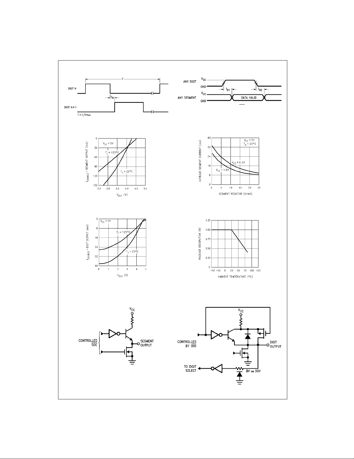
Switching Time Waveforms (Continued)
Multiplexing Output Waveforms Read Data Waveforms
Typical Perf ormance Characteristics
Segment outputs if shorted to groun d w ill exceed maximum
power dissipation of the device.
Note A: All other digit lines are at a low level. DIO at a HIGH lev el.
V
is the saturation voltage of th e digit drive transistor.
CE
Power Dissipation vs
Temperature for
Plastic Packages
MM74C911
Applications
Segment Output Structure Digit Output Structure
5 www.fairchildsemi.com
Page 6
MM74C911
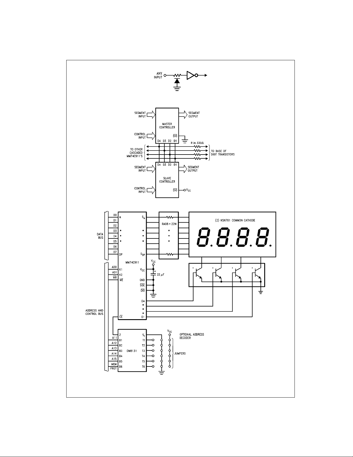
Input Protection
Segment Expansion
Typical Application
*Base resistors may be necessary to limit base current.
www.fairchildsemi.com 6
Page 7
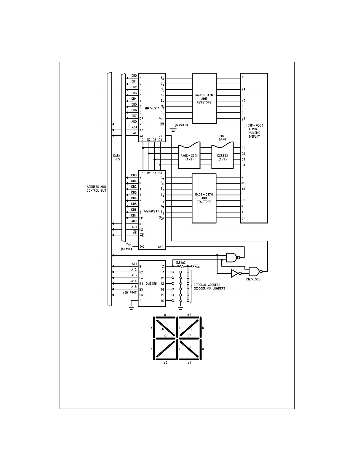
4-Digit, 16-Segment Alpha-Numeric Display
MM74C911
Segment
Identification
7 www.fairchildsemi.com
Page 8
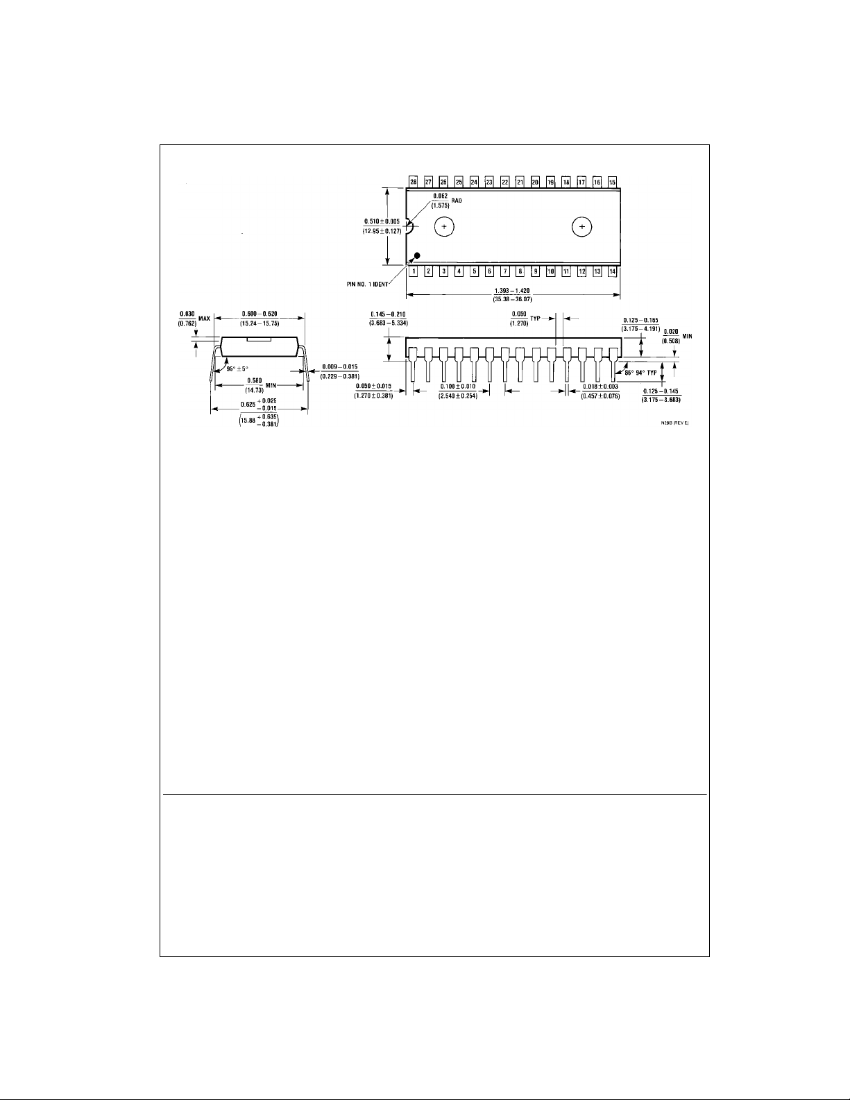
Physical Dimensions in ches (millimeters) unless otherwise noted
28-Lead Plastic Dual-In-Line Package (PDIP), JEDEC MS-010, 0.600” Wide
Package Number N28B
MM74C911 4-Digit Expandable Segment Display Controller
LIFE SUPPORT POLICY
FAIRCHILD’S PRODUCTS ARE NOT AUTHORIZED FOR USE AS CRITICAL COMPONENTS IN LIFE SUPPORT
DEVICES OR SYSTEMS WITHOUT THE EXPRESS WRITTEN APPROVAL OF THE PRESIDENT OF FAIRCHILD
SEMICONDUCTOR CORPORATION. As used herein:
1. Life support devices or systems are devices or syste ms
which, (a) are intended for surgical implant into the
body, or (b) support or sustain life, and (c) whose failure
to perform when properly used in accordance with
instructions for use provided in the labeling, can be reasonably expected to result in a significant injury to the
user.
2. A critic al comp onent in any comp onent of a l ife suppor t
device or system whose failure to perform can be reasonably expected to cause the failure of the life suppor t
device or system, or to affect its safety or effectiveness.
www.fairchildsemi.com
Fairchild does not assume any responsibility for use of any circuitry descri bed, no circuit patent licenses are implied and Fairchild reser ves the right at any time without notice to change said circuitry and specifications.
 Loading...