

Page 1
MM74C908
Dual CMOS 30-Volt Relay Driver
MM74C908 Dual CMOS 30-Volt Relay Driver
October 1987
Revised January 1999
General Description
The MM74C908 is a general purpose dual high voltage
driver capable of sourcing a minimum of 250 mA at V
− 3V, and TJ = 65°C.
V
CC
The MM74C908 consists of two CMOS NAND gates driving an emitter follower Darlin gton output to achieve high
current drive and high voltage capabilities. In the “OFF”
state the outputs can withstand a maximum of −30V across
the device. These CMOS drivers are use ful in interfacing
OUT
normal CMOS voltage levels to driving relays, regulators,
lamps, etc.
=
Features
■ Wide supply voltage range: 3V to 18V
■ High noise immunity: 0.45 V
■ Low output “ON” resistance: 8Ω (typ.)
■ High voltage: −30V
■ High current: 250 mA
CC
(typ.)
Ordering Code:
Order Number Package Number Package Description
MM74C908N N08E 8-Lead Plastic Dual-In-Line Package (PDIP), JEDEC MS-001, 0.300” Wide
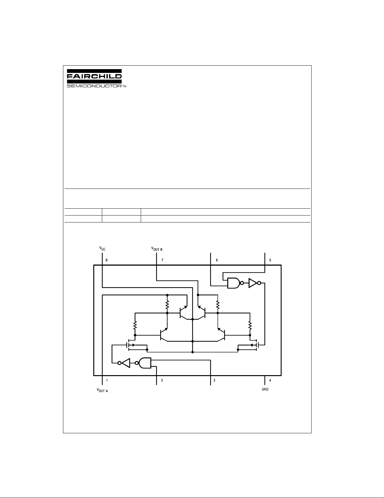
Connection Diagram
Pin Assignments for DIP
Top View
© 1999 Fairchild Semiconductor Corporation DS005912.prf www.fairchildsemi.com
Page 2
Absolute Maximum Ratings(Note 1)
Voltage at any Input Pin −0.3V to VCC +0.3V
Voltage at any Output Pin 32V
Operatin g Temp er at u re Ra ng e −40°C to +85°C
MM74C908
Operating V
Absolute Maximum V
I
SOURCE
Storage Temperature +150°C
Range (T
Range 4V to 18V
CC
CC
) −65°C to +150°C
S
19V
500 mA
Lead Temperature (T
(Soldering, 10 seconds) 260°C
Power Dissipation (P
Note 1: “Absolute Maxi mum Ratings” are those valu es beyond which the
safety of the device cannot be guaranteed. Ex ce pt for “O perating Temperature Range” they are not mean t to imply that the devices sho uld be operated at these limits. The Electrical Charac t eristics table provides co nditions
for actual device operation.
)
L
) Refer to Maximum Power
D
Dissipation vs Ambient
Temperature Graph
DC Electrical Characteristics
Min/Max limits apply across temperature range, unless otherwise noted
Symbol Parameter Conditions Min Typ Max Units
CMOS TO CMOS
V
IN(1)
V
IN(0)
I
IN(1)
I
IN(0)
I
CC
CMOS/LPTTL INTERFA CE
OUTPUT DRIVE
V
OUT
R
ON
θ
JA
Note 2: θJA measured in free air w it h device soldered into print ed circuit board.
Logical “1” Input Voltage VCC = 5V 3.5 V
Logical “0” Input Voltage VCC = 5V 1.5 V
Logical “1” Input Current VCC = 15V, VIN = 15V 0.005 1.0 µA
Logical “0” Input Current VCC = 15V, VIN = 0V −1.0 −0.005 µA
Supply Current VCC = 15V, Outputs Open Circuit 0.05 15 µA
Output “OFF” Voltage VIN = VCC, I
V
Logical “1” Input Voltage VCC = 4.75V VCC − 1.5 V
IN(1)
V
Logical “0” Input Voltage VCC = 4.75V 0.8 V
IN(0)
Output Voltage I
Output Resistance I
Output Resistance 0.55 0.80 %/°C
Coefficient
Thermal Resistance (Note 2) 100 110 °C/W
MM74C908 (Note 2) 45 55 °C/W
VCC = 10V 8.0 V
VCC = 10V 2.0 V
= −200 µA −30 V
OUT
= −300 mA, VCC ≥ 5V, TJ = 25°CVCC−2.7 VCC−1.8 V
OUT
I
= −250 mA, VCC ≥ 5V, TJ = 65°CVCC−3.0 VCC−1.9 V
OUT
I
= −175 mA, VCC ≥ 5V, TJ = 150°C VCC−3.15 VCC−2.0 V
OUT
= −300 mA, VCC ≥ 5V, TJ = 25°C6.09.0Ω
OUT
I
= −250 mA, VCC ≥ 5V, TJ = 65°C7.512Ω
OUT
I
= −175 mA, VCC ≥ 5V, TJ = 150°C1018Ω
OUT
AC Electrical Charac teristics (Note 3)
Symbol Parameter Conditions Min Typ Max Units
t
pd1
t
pd0
C
Note 3: AC Parameters are guara nt eed by DC correlated testing.
Note 4: Capacitance is guaranteed by periodic testing.
www.fairchildsemi.com 2
Propagation Delay VCC = 5V, RL = 50Ω, 150 300 ns
to a Logical “1” CL = 50 pF, TA = 25°C
Propagation Delay VCC = 5V, RL = 50Ω, 2.0 10 µs
to a Logic “0” CL = 50 pF, TA = 25°C
Input Capacitance (Note 4) 5.0 pF
IN
VCC = 10V, RL = 50Ω, 65 120 ns
CL = 50 pF, TA = 25°C
VCC = 10V, RL = 50Ω, 4.0 20 µs
CL = 50 pF, TA = 25°C
Page 3

Typical Performance Charact eristics
MM74C908
Maximum Power Dissipation
vs Ambient Temperature
− V
Maximum V
CC
OUT
vs I
OUT
Typical I
vs Typical V
OUT
OUT
Typical I
Typical I
Typical V
vs Typical V
OUT
OUT
vs
OUT
OUT
AC Test Circuit Switching Time Waveforms
tr = tf = 20 ns
3 www.fairchildsemi.com
Page 4

Power Considerations
Calculating Output “ON” Resistance (RL > 18Ω)
The output “ON” resistance, R
tion temperature, T
MM74C908
= 9 (TJ − 25) (0.008) + 9: (1)
R
ON
is given by:
and T
J
= TA + P
T
J
where T
A
and P
DAV
device. P
= ambient temperature, θJA = thermal resistance,
is the average power dissipated within the
DAV
, and is given by:
J
DAV θJA
consists of normal CMOS power terms (due
,: (2)
, is a function o f the junc -
ON
to leakage currents, i nternal capacitance, switching, etc.)
which are insignifica nt when compare d to the power dissipated in the outputs. Thu s, the output power term defines
the allowable limits of o pe ration a nd in clude s both outputs,
A and B. P
where I
is given by:
D
2
= I
RON + I
P
D
OA
is the output current, given by:
O
2
RON,(3)
OB
(4)
is the load voltage.
V
L
The average power dissipation, P
, is a function of the
DAV
duty cycle:
2
= I
P
DAV
I
OB
RON (Duty CycleA) + (5)
OA
2
RON(Duty CycleB)
where the duty cycle is th e % time in the current sour ce
state. Substituting equations (1) and (5) into (2) yields:
= TA + θJA [9 (TJ − 25) (0.008) + 9]: (6a)
T
J
2
(Duty CycleA) + I
[I
OA
2
(Duty CycleB)]
OB
simplifying:
Equations (1), (4), and (6b) can be used in an iterative
method to determine the output current, output resistance
and junction temperature.
For example, let V
= 0V, TA = 25°C, θJA = 110°C/W, Duty CycleA = 50%,
V
L
Duty Cycle
Assuming R
= 75%.
B
= 11Ω, then:
ON
= 15V, RLA = 100Ω, RLB = 100Ω,
CC
and
Applications
(See AN-177 for applications)
www.fairchildsemi.com 4
= 9 (TJ − 25) (0.008) + 9
and R
ON
= 9(52.6 − 25) (0.008) + 9 = 11Ω
Page 5

Physical Dimensions inches (millimeters) unless otherwise noted
MM74C908 Dual CMOS 30-Volt Relay Driver
8-Lead Plastic Dual-In-Line Package (PDIP), JEDEC MS-001, 0.300” Wide
LIFE SUPPORT POLICY
FAIRCHILD’S PRODUCTS ARE NOT AUTHORIZED FOR USE AS CRITICAL COMPONENTS IN LIFE SUPPORT
DEVICES OR SYSTEMS WITHOUT THE EXPRESS WRITTEN APPROVAL OF THE PRESIDENT OF FAIRCHILD
SEMICONDUCTOR CORPORATION. As used herein:
1. Life support devices or system s a re devices or syste ms
which, (a) are intended for surgical implant into the
body, or (b) support or sustain life, and (c) whose failure
to perform when properly used in accordance with
instructions for use provided in the label in g, can be re asonably expected to result i n a significant injur y to the
user.
Package Number N08E
2. A critical componen t in a ny compon ent of a life support
device or system whose failure to perform can be reasonably expected to cause the failure of the life support
device or system, or to affect its safety or effectiveness.
www.fairchildsemi.com
Fairchild does not assume any responsibility for use of any circuitry described, no circuit patent licenses are implied and Fairchild reserves the right at any time without notice to change said circuitry and specifications.
 Loading...