

Page 1
© 1999 Fairchild Semiconductor Corporation DS005905 www.fairchildsemi.com
October 1987
Revised July 1999
MM74C240 • MM74C244 Inverting • Non-Inverting Octal Buffer and Line Driver with 3-STATE Outputs
MM74C240 • MM74C244
Inverting • Non-Inverting Octal Buffer and
Line Driver with 3-STATE Outputs
General Description
The MM74C240 and MM74C244 octal buffers and line
drivers are monolithic complementary MOS (CMOS) integrated circuits with 3-STATE outputs. These outputs have
been specially designed to drive highly capacitive loads
such as bus-oriented sys tems. These devices have a fan
out of 6 low power Schottky loads. A high logic level on the
output disable contr ol input G makes the outputs go into
the high impedance state.
Features
■ Wide supply voltage range (3V to 15V)
■ High noise immunity (0.45 V
CC
typ)
■ Low power consumption
■ High capacitive load drive capability
■ 3-STATE outputs
■ Input protection
■ TTL compatibility
■ 20-pin dual-in-line package
■ High speed 25 ns (typ.) @ 10V, 50 pF (MM74C244)
Ordering Code:
Devices also availab le in Tape and Reel. Specify by appending su ffix le tter “X” to the ordering code.
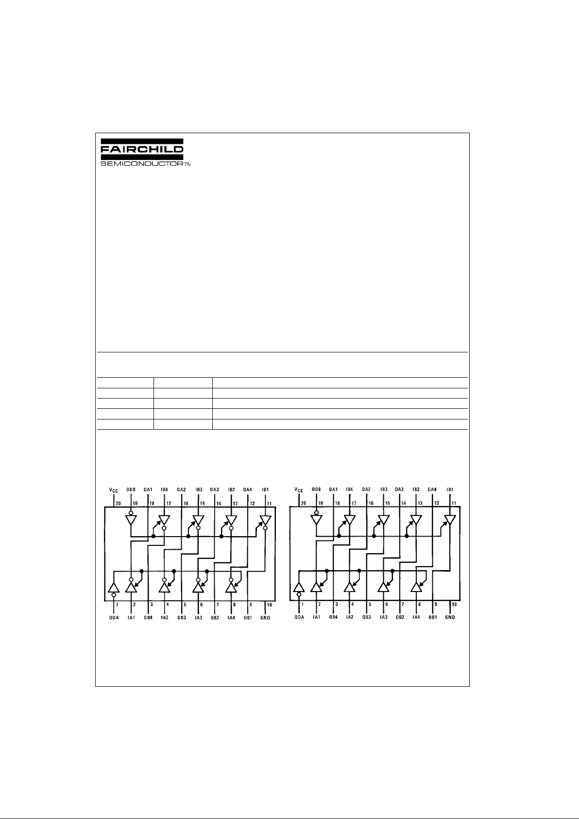
Connection Diagrams
Pin Assignments for DIP and SOIC
MM74C240
(Top View)
MM74C244
(Top View)
Order Number Package Number Package Description
MM74C240WM M20B 20-Lead Small Outline Integrated Circuit (SOIC), JEDEC MS-013, 0.300” Wide Body
MM74C240N N20A 20-Lead Plastic Dual-In-Line Package (PDIP), JEDEC MS-001, 0.300” Wide
MM74C244WM M20B 20-Lead Small Outline Integrated Circuit (SOIC), JEDEC MS-013, 0.300” Wide Body
MM74C244N N20A 20-Lead Plastic Dual-In-Line Package (PDIP), JEDEC MS-001, 0.300” Wide
Page 2
www.fairchildsemi.com 2
MM74C240 • MM74C244
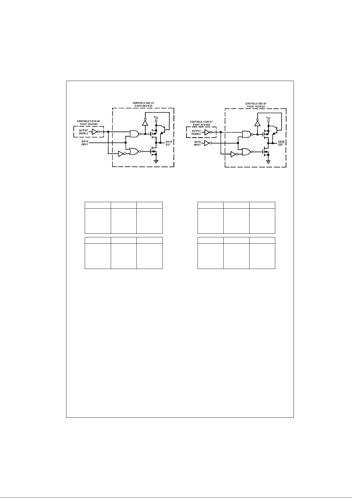
Logic Diagrams
MM74C240 MM74C244
Truth Tables
MM74C240 MM74C244
1 = HIGH
0 = LOW
X = Don’t Care
Z = 3-STATE
ODA IA OA
1XZ
1XZ
001
010
ODB IB OB
1XZ
1XZ
001
010
ODA IA OA
1XZ
1XZ
000
011
ODB IB OB
1XZ
1XZ
000
011
Page 3
3 www.fairchildsemi.com
MM74C240 • MM74C244
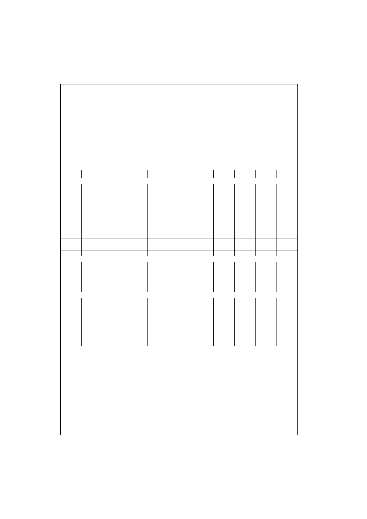
Absolute Maximum Ratings(Note 1)
Note 1: “Absolute Maximum Ratings” are those values beyond which the
safety of the device cannot be guaran teed. Excep t for “Operating Range”
they are not meant to imp ly that the devic es should be opera ted at these
limits. The Elec trical Characteristics table p rovides conditions for act ual
device operation.
DC Electrical Characteristics
Min/Max limits apply across temperature range, unless otherwise noted
Voltage at Any Pin −0.3V to VCC + 0.3V
Operating Temperature Range −40°C to +85°C
Storage Temperature Range −65°C to +150°C
Power Dissipation
Dual-In-Line 700 mW
Small Outline 500 mW
Operating V
CC
Range 3V to 15V
Absolute Maximum V
CC
18V
Lead Temperature
(Soldering, 10 seconds) 260°C
Symbol Parameter Conditions Min Typ Max Units
CMOS TO CMOS
V
IN(1)
Logical “1” Input Voltage VCC = 5V 3.5 V
VCC = 10V 8.0 V
V
IN(0)
Logical “0” Input Voltage VCC = 5V 1.5 V
VCC = 10V 2.0 V
V
OUT(1)
Logical “1” Output Voltage VCC = 5V, I O = −10 µA4.5 V
VCC = 10V, IO = −10 µA9.0 V
V
OUT(0)
Logical “0” Output Voltage VCC = 5V, I O = 10 µA0.5V
VCC = 10V, IO = 10 µA1.0V
I
OZ
3-STATE Output Current VCC = 10V, OD = V
IH
±10 µA
I
IN(1)
Logical “1” Input Current VCC = 15V, VIN = 15V 0.005 1.0 µA
I
IN(0)
Logical “0” Input Current VCC = 15V, VIN = 0V −1.0 −0.005 µA
I
CC
Supply Current VCC = 15V 0.05 300 µA
CMOS/LPTTL INTERFACE
V
IN(1)
Logical “1” Input Voltage VCC = 4.75V VCC − 1.5 V
V
IN(0)
Logical “0” Input Voltage VCC = 4.75V 0.8 V
V
OUT(1)
Logical “1” Output Voltage VCC = 4.75V, IO = −450 µAV
CC
− 0.4 V
VCC = 4.75V, IO = −2.2 mA 2.4 V
V
OUT(0)
Logical “0” Output Voltage VCC = 4.75V, IO = 2.2 mA 0.4 V
OUTPUT DRIVE (See Family Characteristics Data Sheet) (Short Circuit Current)
I
SOURCE
Output Source Current VCC = 5V, V
OUT
= 0V −14 −30 mA
(P-Channel) TA = 25°C
VCC = 10V, V
OUT
= 0V −36 −70 mA
TA = 25°C
I
SINK
Output Sink Current VCC = 5V, V
OUT
= V
CC
12 20 mA
(N-Channel) TA = 25°C
VCC = 10V, V
OUT
= V
CC
48 70 mA
TA = 25°C
Page 4

www.fairchildsemi.com 4
MM74C240 • MM74C244
AC Electrical Characteristics (Note 2)
T
A
= 25°C, C
L
= 50 pF, unless otherwise specified
Note 2: AC Parame t ers are guaranteed by DC c orrelated testing.
Note 3: C
PD
determines th e no loa d AC p ower c onsump tion of any C MOS d evice. F or co mplete e xplana tion s ee Fami ly Cha racteris tics Ap plication Note,
AN-90.
Note 4: Capacitanc e is guaranteed by pe riodic testing.
Symbol Parameter Conditions Min Typ Max Units
t
PD(1)
,
t
PD(0)
Propagation Delay
(Data In to Out)
MM74C240 VCC = 5V, CL = 50 pF 60 90 ns
VCC = 10V, CL = 50 pF 40 70 ns
V
CC
= 5V, CL = 150 pF 80 110 ns
VCC = 10V, CL = 150 pF 60 90 ns
MM74C244 V
CC
= 5V, CL = 50 pF 45 70 ns
VCC = 10V, CL = 50 pF 25 50 ns
VCC = 5V, CL = 150 pF 60 90 ns
VCC = 10V, CL = 150 pF 40 70 ns
t1H, t
0H
Propagation Delay Output RL = 1k, CL = 50 pF
Disable to High Impedance VCC = 5V 45 80 ns
State (from a Logic Level) VCC = 10V 35 60 ns
tH1, t
H0
Propagation Delay Output RL = 1k, CL = 50 pF
Disable to Logic Level VCC = 5V 50 90 ns
(from High Impedance State) VCC = 10V 30 60 ns
t
T(HL)
, t
T(LH)
Transition Time VCC = 5V, CL = 50 pF 45 80 ns
VCC = 10V, CL = 50 pF 30 60 ns
VCC = 5V, CL = 150 pF 75 140 ns
VCC = 10V, CL = 150 pF 50 100 ns
C
PD
Power Dissipation (Note 3)
Capacitance
(Output Enabled per Buffer)
MM74C240 100 pF
MM74C244 100 pF
(Output Disabled per Buffer)
MM74C240 10 pF
MM74C244 0pF
C
IN
Input Capacitance (Note 4) VIN = 0V, f = 1 MHz, TA = 25°C 10 pF
(Any Input)
C
O
Output Capacitance (Note 4) VIN = 0V, f = 1 MHz, TA = 25°C 10 pF
(Output Disabled)
Page 5

5 www.fairchildsemi.com
MM74C240 • MM74C244
Typical Application
Typical Performance Characteristics
N-Channel Output Drive at 25°C
MM74C240
Propagation Delay vs. Load Capacitance
P-Channel Output Drive at 25°C
MM74C244
Propagation Delay vs. Load Capacitance
Page 6

www.fairchildsemi.com 6
MM74C240 • MM74C244
AC Test Circuits and Switching Time Waveforms
t
pd0, tpd1
t1H and t
H1
t0H and t
H0
Note: Delays measured with input tr, tf ≤ 20 ns.
CMOS to CMOS t1H and t
H1
Note: VOH is defined as the DC output hig h voltage when the device is
loaded with a 1 kΩ resistor t o ground.
t
OH
and t
H0
Note: VOL is defined as the DC output low voltage when the device is loaded with a 1 kΩ resistor to VCC.
Page 7

7 www.fairchildsemi.com
MM74C240 • MM74C244
Physical Dimensions inches (millimeters) unless otherwise noted
20-Lead Small Outline Integrated Circuit (SOIC), JEDEC MS-013, 0.300” Wide Body
Package Number M20B
Page 8

www.fairchildsemi.com 8
MM74C240 • MM74C244 Inverting • Non-Inverting Octal Buff er and Line Driver with 3-STATE Outputs
Physical Dimensions inches (millimeters) unless otherwise noted (Continued)
20-Lead Plastic Dual-In-Line Package (PDIP), JEDEC MS-001, 0.300” Wide
Package Number N20A
Fairchild does not assume any responsibility for use of any circuitry described, no circuit pate nt licenses are implied and
Fairchild reserves the right at any time without notice to change said circuitry and specifications.
LIFE SUPPORT POLICY
FAIRCHILD’S PRODUCTS ARE NOT AUTHORIZED FOR USE AS CRITICAL COMPONENTS IN LIFE SUPPORT
DEVICES OR SYSTEMS WITHOUT THE EXPRESS WRITTEN APPROVAL OF THE PRESIDENT OF FAIRCHILD
SEMICONDUCTOR CORPORATION. As used herein:
1. Life support devices or systems are devices or syste ms
which, (a) are intended for surgical implant into the
body, or (b) support or sustain life, and (c) whose failure
to perform when properly used in accordance with
instructions for use provided in the labeling, can be reasonably expected to result in a significant inju ry to the
user.
2. A critical component i n any compon ent of a lif e support
device or system whose failu re to perform can be reasonably expected to ca use the fa i lure of the life su pp ort
device or system, or to affect its safety or effectiveness.
www.fairchildsemi.com
 Loading...