

Page 1
查询74C221供应商
MM74C221
Dual Monostable Multivibrator
MM74C221 Dual Monostable Multivibrator
November 1987
Revised January 1999
General Description
The MM74C221 dual monostable multivibrator is a monolithic complementary MOS integrated circuit. Each multivibrator features a negative-transit ion-triggered input and a
positive-transition-triggered input, either of which can be
used as an inhibit input, and a clear input.
Once fired, the ou tput pulses are independen t of further
transitions of the A a nd B input s and are a fu nction of t he
external timing components C
width is stable over a wide range of temperature and V
EXT
and R
. The pulse
EXT
Pulse stability will be limited by the accuracy of external
timing components. The pulse width is approximately
defined by the relati onship t
ther information and applications, see AN-138.
W(OUT)
≈ C
Features
■ Wide supply voltage range: 4.5V to 15V
■ Guaranteed noise margin: 1.0V
■ High noise immunity: 0.45 V
.
CC
■ Low power TTL compatibility: fan out of 2 driving 74L
CC
(typ.)
EXT REXT
Ordering Code:
Order Number Package Number Package Description
74MMC221N N16E 16-Lead Plastic Dual-in-Line Package (PDIP), JEDEC MS-001, 0.300” Wide
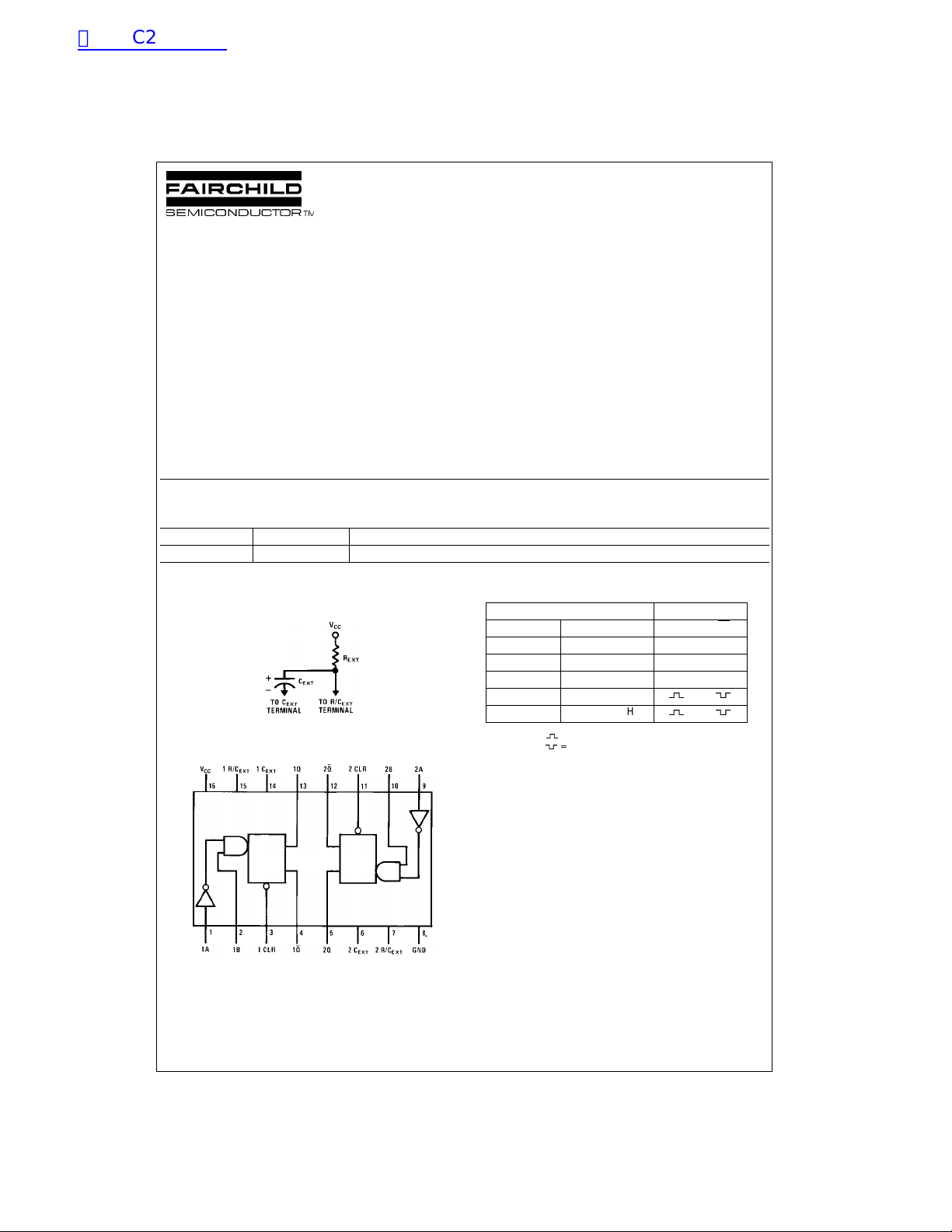
Connection Diagrams
Timing Component
Pin Assignments for DIP
Truth Table
Inputs Outputs
Clear A B Q Q
LX XLH
X HXLH
XXLLH
HL↑
H ↓ H
H = HIGH Level = One HIGH level pulse
L = LOW Level
↑ = Transition from LOW-to-HIGH X= I rrelevant
↓ = Transition from HIGH-to-LOW
= One LOW le vel pulse
. For fur-
Top View
© 1999 Fairchild Semiconductor Corporation DS005904.prf www.fairchildsemi.com
Page 2
Absolute Maximum Ratings(Note 1)
Voltage at Any Pin −0.3V to VCC + 0.3V
Operating Temperature Range −40°C to +85°C
Storage Temperature Range −65°C to +150°C
MM74C221
Power Dissipation
Dual-In-Line 700 mW
Small Outline 500 mW
Operating V
Range 4.5V to 15V
CC
Absolute Maximum V
≥ 80 VCC (Ω)
R
EXT
CC
Lead Temperature
(Soldering, 10 seconds) 260°C
Note 1: “Absolute Maxi mum Ratings” are those valu es beyond which the
safety of the device cannot be guaranteed. Ex ce pt for “O perating Temperature Range” they are not mean t to imply that the devices sho uld be operated at these limits. The Electrical Charac t eristics table provides co nditions
for actual device operation.
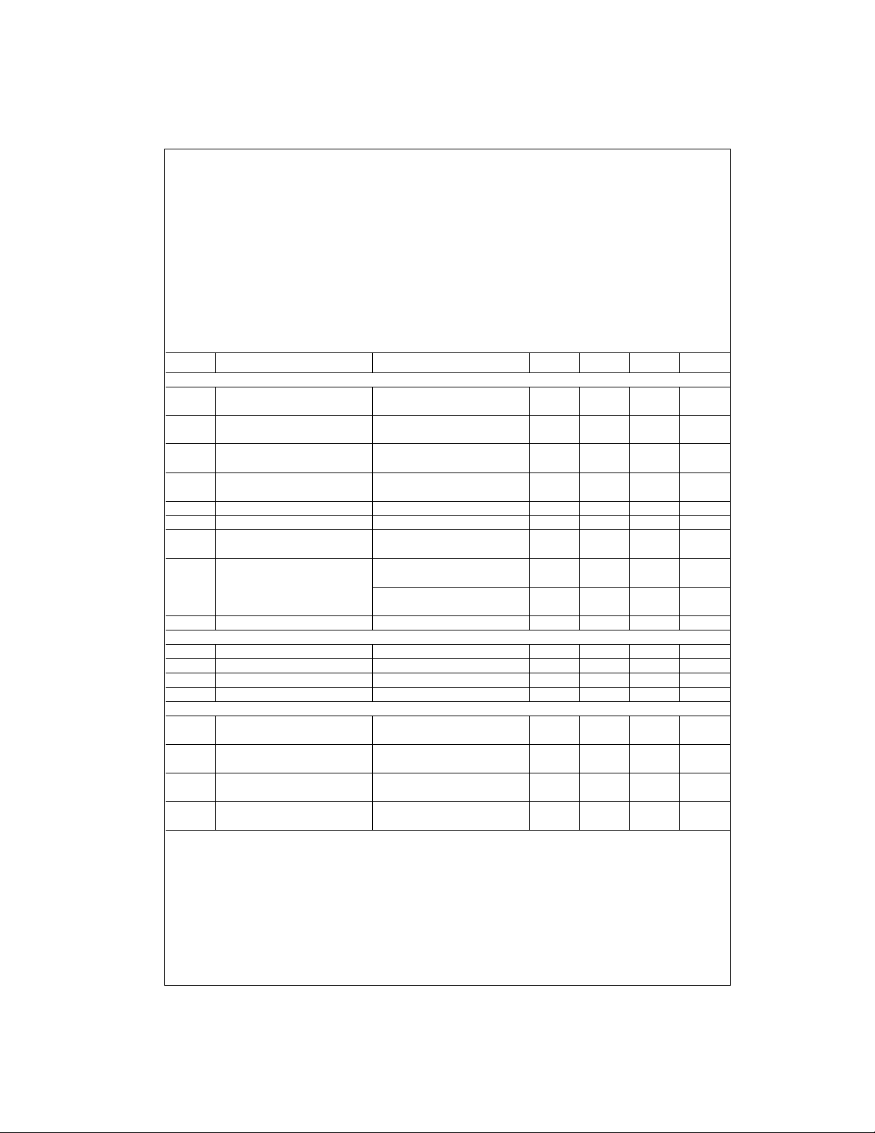
DC Electrical Characteristics
Max/min limits apply across temperature range, unless otherwise noted
Symbol Parameter Conditions Min Typ Max Units
CMOS to CMOS
V
IN(1)
V
IN(0)
V
OUT(1)
V
I
IN(1)
I
IN(0)
I
CC
I
CC
CMOS/LPTTL Interface
V
IN(1)
V
IN(0)
V
OUT(1)
V
Output Drive (See Family Characteristics Data Sheet) (Short Circuit Current)
I
SOURCE
I
SOURCE
I
SINK
I
SINK
Note 2: In Standby (Q = Logic “0”) the power dissi pated equals the leakage current plus VCC/R
OUT(0)
OUT(0)
Logical “1” Input Voltage VCC = 5V 3.5 V
VCC = 10V 8.0 V
Logical “0” Input Voltage VCC = 5V 1.5 V
VCC = 10V 2.0 V
Logical “1” Output Voltage VCC = 5V, IO = −10 µA 4.5 V
VCC = 10V, IO = −10 µA 9.0 V
Logical “0” Output Voltage VCC = 5V, IO = +10 µA 0.5V
VCC = 10V, IO = +10 µA 1V
Logical “1” Input Current VCC = 15V, VIN = 15V 0.005 1.0 µA
Logical “0” Input Current VCC = 15V, VIN = 0V −1.0 −0.005 µA
Supply Current (Standby) VCC = 15V, R
= ∞, 0.05 300 µA
EXT
Q1, Q2 = Logic “0” (Note 2)
Supply Current VCC = 15V, Q1 = Logic “1”, 15 mA
(During Output Pulse) Q2 = Logic “0” (Figure 4)
VCC = 5V, Q1 = Logic “1”, 2 mA
Q2 = Logic “0” (Figure 4)
Leakage Current at R/C
Logical “1” Input Voltage V
Pin VCC = 15V, V
EXT
CC
= 5V 0.01 3.0 µA
CEXT
= 4.75V VCC − 1.5 V
Logical “0” Input Voltage VCC = 4.75V 0.8 V
Logical “1” Output Voltage V
= 4.75V, IO = −360 µA 2.4 V
CC
Logical “0” Output Voltage VCC = 4.75V, IO = 360 µA 0.4V
Output Source Current VCC = 5V −1.75 mA
(P-Channel) TA = 25°C, V
OUT
= 0V
Output Source Current VCC = 10V −8 mA
(P-Channel) TA = 25°C, V
OUT
= 0V
Output Sink Current VCC = 5V 1.75 mA
(N-Channel) TA = 25°C, V
OUT
= V
CC
Output Sink Current VCC = 10V 8 mA
(N-Channel) TA = 25°C, V
OUT
= V
CC
EXT
.
18V
www.fairchildsemi.com 2
Page 3
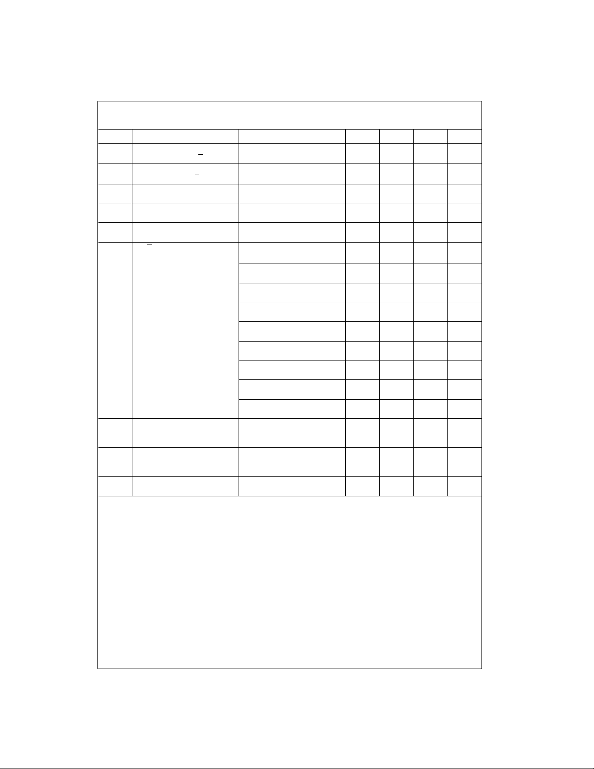
AC Electrical Characteristics (Note 3)
= 25°C, CL = 50 pF, unless otherwise noted
T
A
Symbol Parameter Conditions Min Typ Max Units
t
pd A, B
t
pd CL
t
S
t
W(A, B)
t
W(CL)
t
W(OUT)
R
C
IN
Note 3: AC Parameters are guaranteed by DC correlated testing.
Note 4: See AN-138 for detailed explanation R
Note 5: Maximum output duty cycle = R
Note 6: Capacitance is guaranteed by periodic testing.
Propagation Delay from Trigger VCC = 5V 250 500 ns
Input (A, B) to Output Q, Q
VCC = 10V 120 250 ns
Propagation Delay from Clear VCC = 5V 250 500 ns
Input (CL) to Output Q, Q
VCC = 10V 120 250 ns
Time Prior to Trigger Input (A, B) VCC = 5V 150 50 ns
that Clear must be Set VCC = 10V 60 20 ns
Trigger Input (A, B) Pulse Width VCC = 5V 150 50 ns
VCC = 10V 70 30 ns
Clear Input (CL) Pulse Width VCC = 5V 150 50 ns
VCC = 10V 70 30 ns
Q or Q Output Pulse Width
VCC = 5V, R
C
EXT
VCC = 10V, R
C
EXT
VCC = 15V, R
C
EXT
VCC = 5V, R
C
EXT
VCC = 10V, R
C
EXT
VCC = 15V, R
C
EXT
VCC = 5V, R
C
EXT
VCC = 10V, R
C
EXT
VCC = 15V, R
C
ON Resistance of Transistor VCC = 5V (Note 4) 50 150 Ω
ON
between R/C
EXT
to C
EXT
EXT
VCC = 10V (Note 4) 25 65 Ω
EXT
= 10k,
900 ns
= 0 pF
= 10k, 350 ns
EXT
= 0 pF
= 10k, 320 ns
EXT
= 0 pF
= 10k, 9.0 10.6 12.2 µs
EXT
= 1000 pF (Figure 1)
= 10k, 9.0 10 11 µs
EXT
= 1000 pF (Figure 1)
= 10k, 8.9 9.8 10.8 µs
EXT
= 1000 pF (Figure 1)
= 10k, 900 1020 1200 µs
EXT
= 0.1 µF (Figure 3)
= 10k, 900 1000 1100 µs
EXT
= 0.1 µF (Figure 3)
= 10k, 900 990 1100 µs
EXT
= 0.1 µF (Figure 3)
VCC = 15V (Note 4) 16.7 45 Ω
Output Duty Cycle R = 10k, C = 1000 pF 90 %
R = 10k, C = 0.1 µF 90%
(Note 5)
Input Capacitance R/C
Input (Note 6) 15 25 pF
EXT
Any Other Input (Note 6) 5 pF
.
ON
+ 1000.
EXT/REXT
MM74C221
3 www.fairchildsemi.com
Page 4
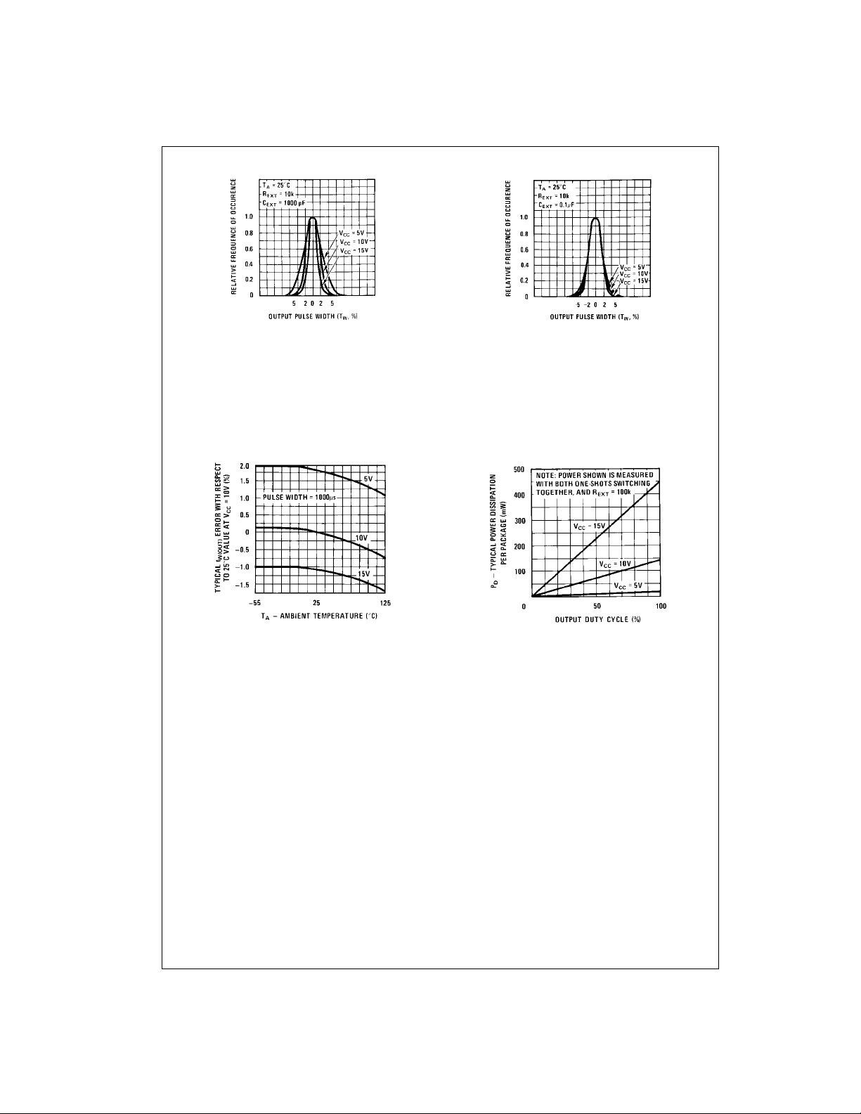
Typical Performance Characteristics
MM74C221
0% Point pulse width:
= 5V, TW = 10.6 µs
At V
CC
= 10V,TW = 10 µs
At V
CC
= 15V,TW = 9.8 µs
At V
CC
Percentage of units within +4%:
= 5V,90% of units
At V
CC
At V
= 10V,95% of units
CC
At V
= 15V,98% of units
CC
FIGURE 1. Typical Distribution of Units for Output
Pulse Width
FIGURE 2. Typical Variation in Output Pulse Width vs
Temperature
0% Point pulse width:
= 5V, TW = 1020 µs
At V
CC
= 10V,TW = 1000 µs
At V
CC
At V
= 15V,TW = 982 µs
CC
Percentage of units within +4%:
= 5V,95% of units
At V
CC
At V
= 10V,97% of units
CC
At V
= 15V,98% of units
CC
FIGURE 3. Typical Distribution of Units for Output
Pulse Width
FIGURE 4. Typical Power Dissipation per Package
www.fairchildsemi.com 4
Page 5
Typical Performance Characteristics (Continued)
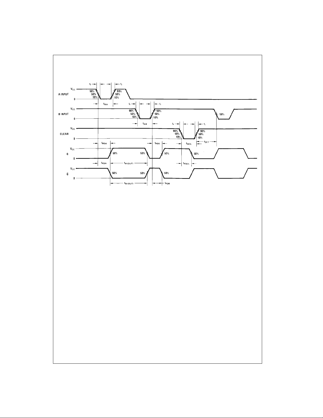
Switching Time Waveforms
tr = tf = 20 ns
MM74C221
5 www.fairchildsemi.com
Page 6
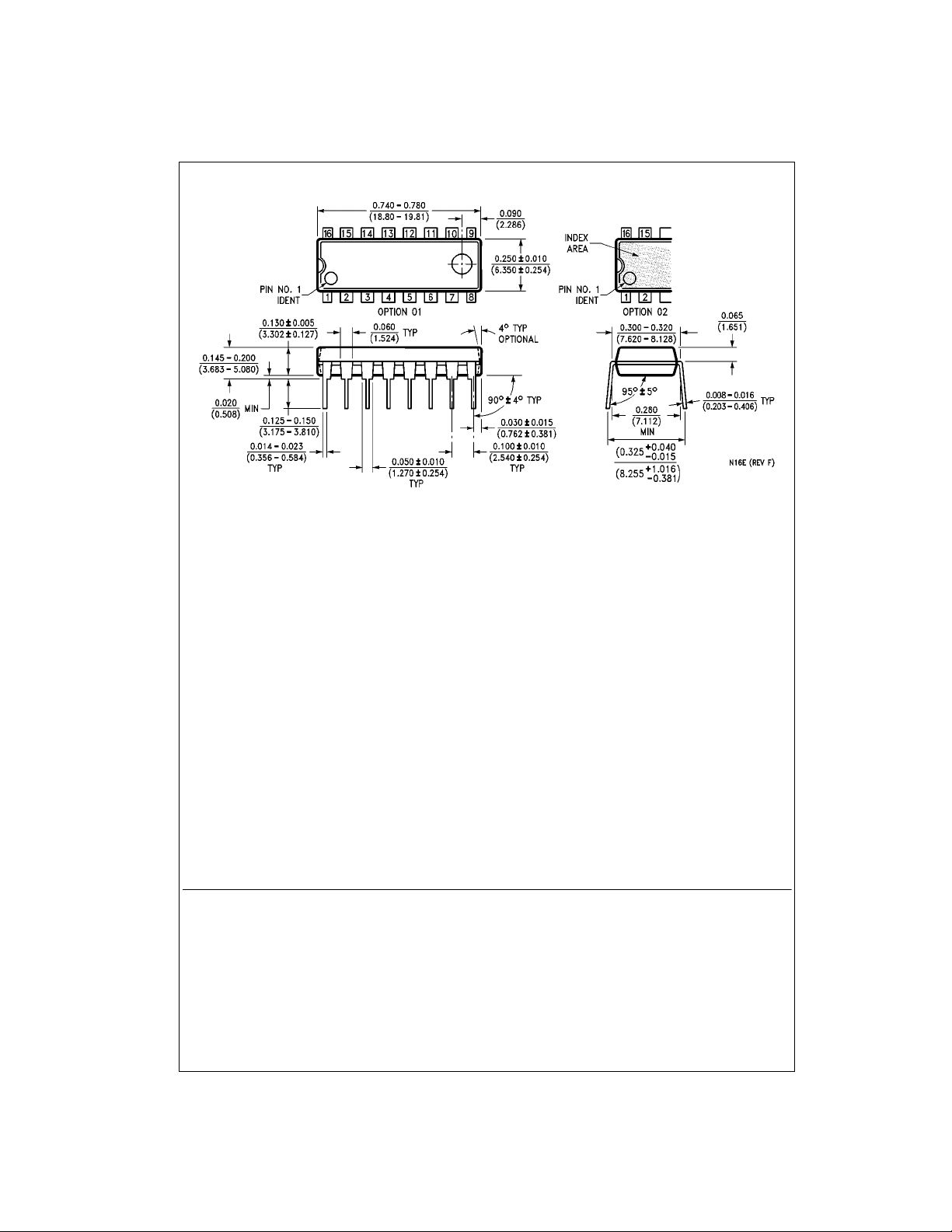
Physical Dimensions in ches (millimeters) unless otherwise noted
MM74C221 Dual Monostable Multivibrator
LIFE SUPPORT POLICY
FAIRCHILD’S PRODUCTS ARE NOT AUTHORIZED FOR USE AS CRITICAL COMPONENTS IN LIFE SUPPORT
DEVICES OR SYSTEMS WITHOUT THE EXPRESS WRITTEN APPROVAL OF THE PRESIDENT OF FAIRCHILD
SEMICONDUCTOR CORPORATION. As used herein:
1. Life support devices or system s ar e devices or syste ms
which, (a) are intended for surgical implant into the
body, or (b) support or sustain life, and (c) whose failure
to perform when properly used in accordance with
instructions for use provided in the labeling, can be reasonably expected to result in a significant injury to the
user.
16-Lead Plastic Dual-In-Line Package (PDIP), JEDEC MS-001, 0.300” Wide
Package Number N16E
2. A critical component in a ny compon ent of a life suppor t
device or system whose failure to perform can be reasonably expected to cause the failure of the life suppor t
device or system, or to affect its safety or effectiveness.
www.fairchildsemi.com
Fairchild does not assume any responsibility for use of any circuitry described, no circuit patent licenses are implied and Fairchild reser ves the right at any time without notice to change said circuitry and specifications.
 Loading...