

Page 1
October 1987
Revised January 1999
MM74C175 Quad D-Type Flip-Flop
© 1999 Fairchild Semiconductor Corporation DS005900.prf www.fairchildsemi.com
MM74C175
Quad D-Type Flip-Flop
General Description
The MM74C175 consis ts of four po si tive-edge tr ig ger ed D type flip-flops implemented with monolithic CMOS technology. Both are true and compleme nted outputs from each
flip-flop are externally available. All four flip-flops are controlled by a common clock and a common clear. Information at the D-type inputs meeting the set-up time
requirements is transferred t o the Q outputs on the positive-going edge of the clock pulse. The clear ing op eration,
enabled by a negative pulse at Clear input, clears all four Q
outputs to logical “0” and Q's to logical “1”.
All inputs are protected from static discharge by diode
clamps to V
CC
and GND.
Features
■ Wide supply voltage range: 3V to 15V
■ Guaranteed noise margin: 1.0V
■ High noise immunity: 0.45 V
CC
(typ.)
■ Low power TTL compatibility: Fan out of 2 driving 74L
Ordering Code:
Device also available in Tape and Reel. Specify by appendin g s uf f ix let t er “X” to the ordering co de.
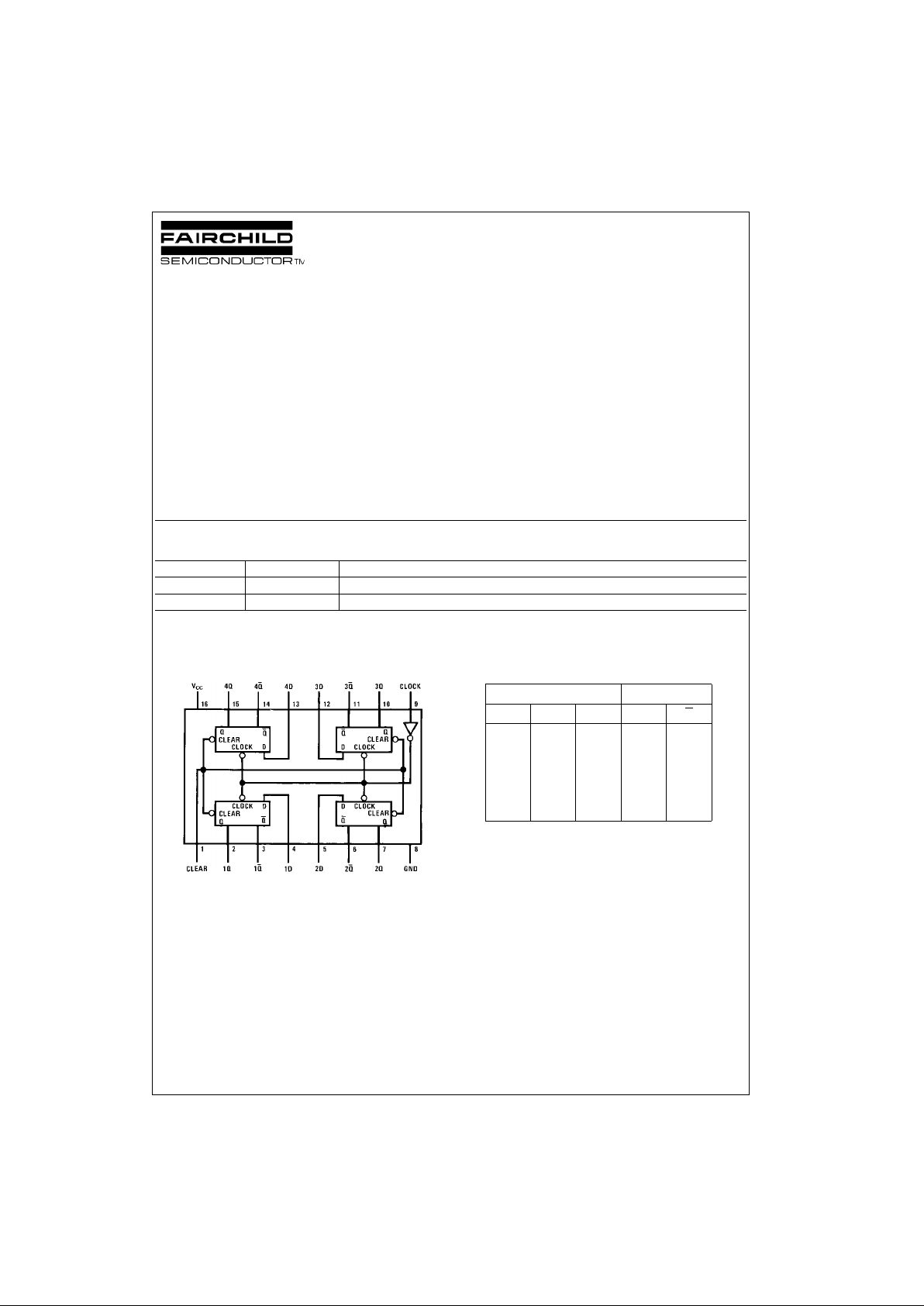
Connection Diagram
Pin Assignments for DIP and SOI C
Top View
Truth Table
Each Flip-Flop
H = HIGH Level
L = LOW Level
X = Irrelevant
↑ = Transition from LOW-to-HIGH level
NC = No Change
Order Number Package Number Package Description
MM74C175M M16A 16-Lead Small Outline Integrated Circuit (SOIC), JEDEC MS-012, 0.150” Narrow
MM74C175N N16E 16-Lead Plastic Dual-In-Line Package (PDIP), JEDEC MS-001, 0.300” Wide
Inputs Outputs
Clear Clock D Q Q
LXXLH
H ↑ HHL
H ↑ LLH
HHXNCNC
HLXNCNC
Page 2
www.fairchildsemi.com 2
MM74C175
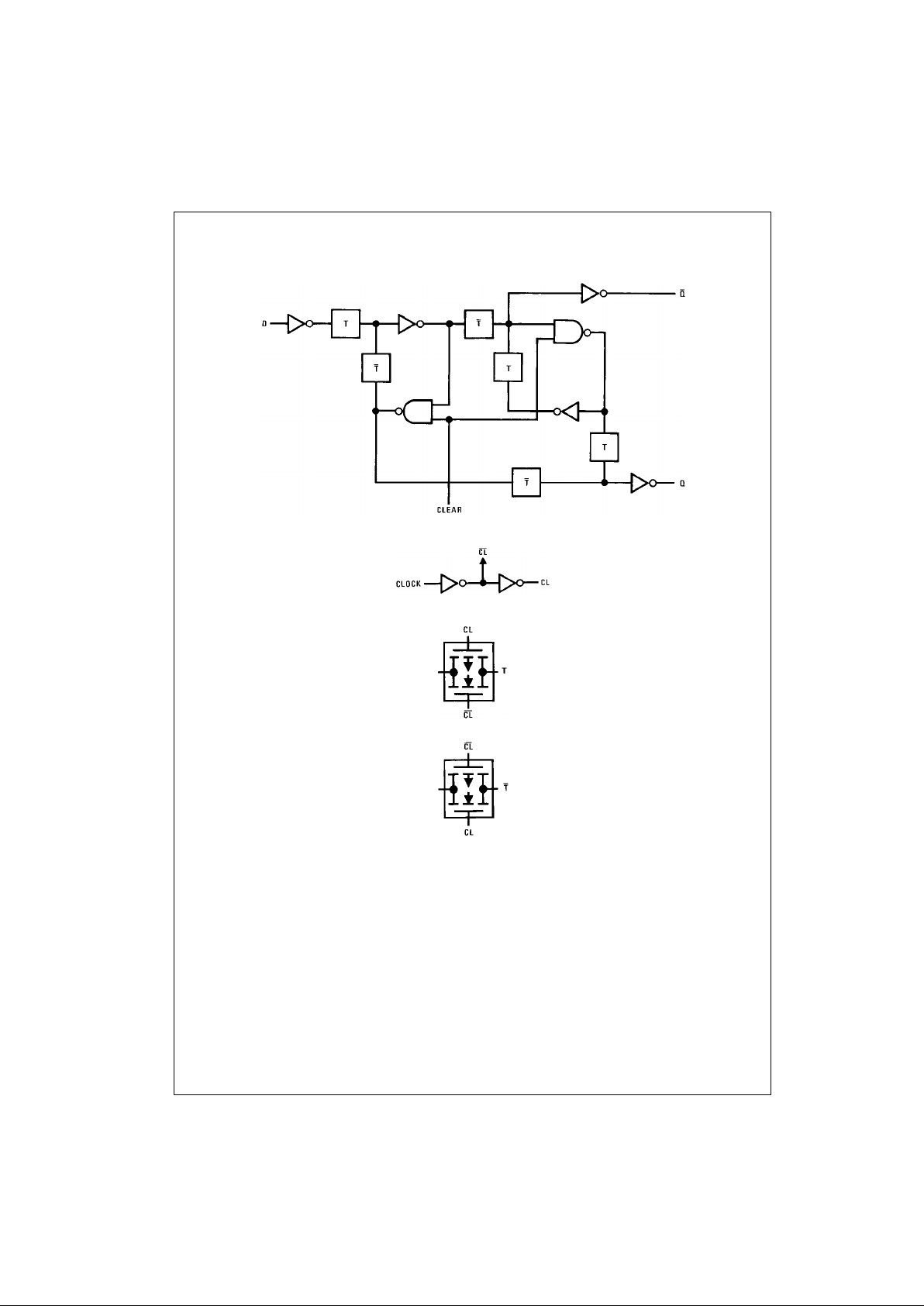
Block Diagrams
Typical One of Four
Page 3

3 www.fairchildsemi.com
MM74C175
Absolute Maximum Ratings(Note 1)
Note 1: “Absolute Maximum Rat ings” are tho se values beyond which the
safety of the device cannot be guaranteed. E x c ept for “ Operating Temperature Range” they are not mea nt to imply that the devices sh ould be operated at these limits. The Electrical Charac t eristics table provide s c onditions
for actual device operation.
DC Electrical Characteristics
Min/Max limits apply across temperature range unless otherwise specified
Voltage at Any Pin −0.3V to VCC +0.3V
Operating Temperature Range −40°C to +85°C
Storage Temperature Range −65°C to +150°C
Power Dissipation (P
D
)
Dual-In-Line 700 mW
Small Outline 500 mW
Operating V
CC
Range 3V to 15V
Absolute Maximum V
CC
18V
Lead Temperature
(Soldering, 10 seconds) 260°C
Symbol Parameter Conditions Min Typ Max Units
CMOS TO CMOS
V
IN(1)
Logical “1” Input Voltage VCC = 5V 3.5 V
VCC = 10V 8.0 V
V
IN(0)
Logical “0” Input Voltage VCC = 5V 1.5 V
VCC = 10V 2.0 V
V
OUT(1)
Logical “1” Output Voltage VCC = 5V, IO = −10 µA4.5 V
VCC = 10V, IO = −10 µA9.0 V
V
OUT(0)
Logical “0” Output Voltage VCC = 5V, IO = 10 µA0.5V
VCC = 10V, IO = 10 µA1.0V
I
IN(1)
Logical “1” Input Current VCC = 15V, VIN = 15V 0.005 1.0 µA
I
IN(0)
Logical “0” Input Current VCC = 15V, VIN = 0V −1.0 −0.005 µA
I
CC
Supply Current VCC = 15V 0.05 300 µA
CMOS/LPTTL INTERFACE
V
IN(1)
Logical “1” Input Voltage 74C, VCC = 4.75V VCC − 1.5 V
V
IN(0)
Logical “0” Input Voltage 74C, VCC = 4.75V 0.8 V
V
OUT(1)
Logical “1” Output Voltage 74C, VCC = 4.75V, IO = −360 µA2.4 V
V
OUT(0)
Logical “0” Output Voltage 74C, VCC = 4.75V, IO = 360 µA0.4V
OUTPUT DRIVE (See Family Characteristics Data Sheet) (Short Circuit Current)
I
SOURCE
Output Source Current VCC = 5V, TA = 25°C, −1.75 −3.3 mA
(P-Channel) V
OUT
= 0V
I
SOURCE
Output Source Current VCC = 10V, TA = 25°C, −8.0 −15 mA
(P-Channel) V
OUT
= 0V
I
SINK
Output Sink Current VCC = 5V, TA = 25°C, 1.75 3.6 mA
(N-Channel) V
OUT
= V
CC
I
SINK
Output Sink Current VCC = 10V, TA = 25°C, 8.0 16 mA
(N-Channel) V
OUT
= V
CC
Page 4

www.fairchildsemi.com 4
MM74C175
AC Electrical Charac teristics (Note 2)
T
A
= 25°C, CL = 50 pF, unless otherwise noted
Note 2: AC Parameters are guara nt eed by DC correlated testing.
Note 3: Capacitance is guaranteed by periodic testing.
Note 4: C
PD
determines the no load AC power consumption of any C M OS device. For complete explanation see Family Characteristics Application Note
AN-90.
Switching Time Waveforms
CMOS to CMOS
Symbol Parameter Conditions Min Typ Max Units
t
pd
Propagation Delay Time to VCC = 5V 190 300 ns
a Logical “0” or Logical “1” from VCC = 10V 75 110 ns
Clock to Q or Q
t
pd
Propagation Delay Time to a VCC = 5V 180 300 ns
Logical “0” from Clear to Q VCC = 10V 70 110 ns
t
pd
Propagation Delay Time to a VCC = 5V 230 400 ns
Logical “1” from Clear to Q VCC = 10V 90 150 ns
t
S
Time Prior to Clock Pulse that VCC = 5V 100 45 ns
Data Must be Present VCC = 10V 40 16 ns
t
H
Time After Clock Pulse that VCC = 5V 0 −11 ns
Data Must be Held VCC = 10V 0 −4ns
t
W
Minimum Clock Pulse Width VCC = 5.0V 130 250 ns
VCC = 10V 45 100 ns
t
W
Minimum Clear Pulse Width VCC = 5.0V 120 250 ns
VCC = 10V 45 100 ns
t
r
Maximum Clock Rise Time VCC = 5V 15 450 µs
VCC = 10V 5.0 125 µs
t
f
Maximum Clock Fall Time VCC = 5V 15 50 µs
VCC = 10V 5.0 50 µs
f
MAX
Maximum Clock Frequency VCC = 5V 2.0 3.5 MHz
VCC = 10V 5.0 10 MHz
C
IN
Input Capacitance Clear Input (Note 3) 10 pF
Any Other Input 5.0 pF
C
PD
Power Dissipation Capacitance Per Package (Note 4) 130 pF
Page 5

5 www.fairchildsemi.com
MM74C175
Physical Dimensions inches (millimeters) unless otherwise noted
16-Lead Small Outline Integrated Circuit (SOIC), JEDEC MS-012, 0.150” Narrow
Package Number M16A
Page 6

Fairchild does not assume any responsibility for use of any circuitry described, no circuit patent licenses are implied and Fairchild reserves the right at any time without notice to change said circuitry and specifications.
MM74C175 Quad D-Type Flip-Flop
LIFE SUPPORT POLICY
FAIRCHILD’S PRODUCTS ARE NOT AUTHORIZED FOR USE AS CRITICAL COMPONENTS IN LIFE SUPPORT
DEVICES OR SYSTEMS WITHOUT THE EXPRESS WRITTEN APPROVAL OF THE PRESIDENT OF FAIRCHILD
SEMICONDUCTOR CORPORATION. As used herein:
1. Life support devices or system s ar e devices or syste ms
which, (a) are intended for surgical implant into the
body, or (b) support or sustain life, and (c) whose failure
to perform when properly used in accordance with
instructions for use provided in the labeling, can be reasonably expected to result in a significant injury to the
user.
2. A critical component in any c omponent of a life suppor t
device or system whose failure to perform can be reasonably expected to cause the failure of the life suppor t
device or system, or to affect its safety or effectiveness.
www.fairchildsemi.com
Physical Dimensions inches (millimeters) unless otherwise noted (Continued)
16-Lead Plastic Dual-In-Line Package (PDIP), JEDEC MS-001, 0.300” Wide
Package Number N16E
 Loading...