

Page 1
October 1987
Revised January 1999
MM74C164 8-Bit Parallel-Out Serial Shift Register
© 1999 Fairchild Semiconductor Corporation DS005896.prf www.fairchildsemi.com
MM74C164
8-Bit Parallel-Out Serial Shift Register
General Description
The MM74C164 shift registers are a monolithic complementary MOS (CMOS ) integrated circuit constructed w ith
N- and P-channel enhancement transistors. These 8-bit
shift registers have gated serial inputs and clear. Each register bit is a D-type master/slave flip-flop. A high-level input
enables the other input which will then determine the state
of the flip-flop.
Data is serially shifted in and out of the 8-bit register during
the positive going transition of c lock pulse. Clear is independent of the clock and accomplished by a low level at the
clear input. All inputs are protected against electrostatic
effects.
Features
■ Supply voltage range: 3V to 15V
■ Tenth power TTL comp atible: drive 2 LPTTL loads
■ High noise immunity: 0.45 V
CC
(typ.)
■ Low power: 50 nW (typ.)
■ Medium speed operation: 0.8 MHz (typ.) with 10V
supply
Applications
• Data terminals
• Instrumentation
• Medical electronics
• Alarm systems
• Industrial electronics
• Remote metering
• Computers
Ordering Code:
Devices also available in Tape and Reel. Specify by appending the suffix letter “X” to t he ordering code.
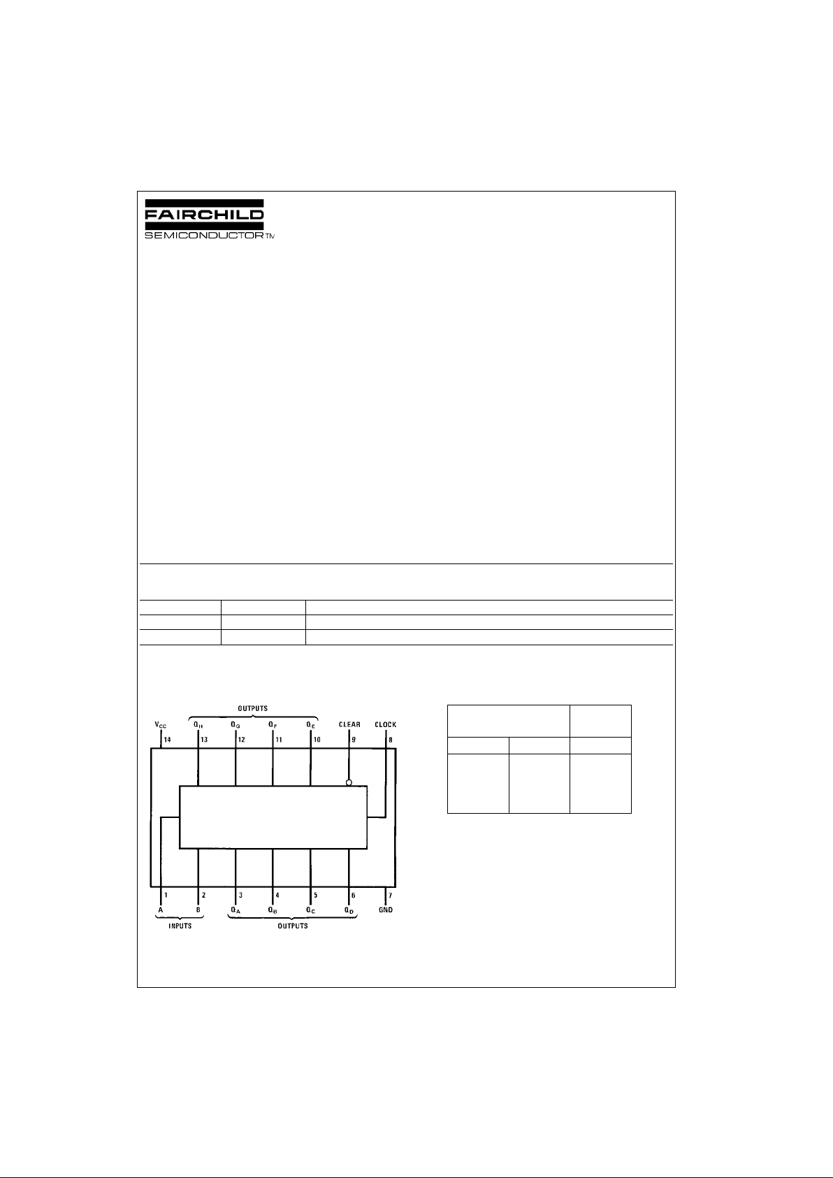
Connection Diagram
Pin Assignments for DIP and SOIC
Top View
Truth Table
Serial Inputs A and B
Order Number Package Number Package Description
MM74C164M M14A 14-Lead Small Outline Integrated Circuit (SOIC), JEDEC MS-120, 0.150” Narrow
MM74C164N N14A 14-Lead Plastic Dual-In-Line (PDIP), JEDEC MS-001, 0.300” Wide
Inputs Output
t
n
t
n+1
ABQ
A
111
010
100
000
Page 2
www.fairchildsemi.com 2
MM74C164
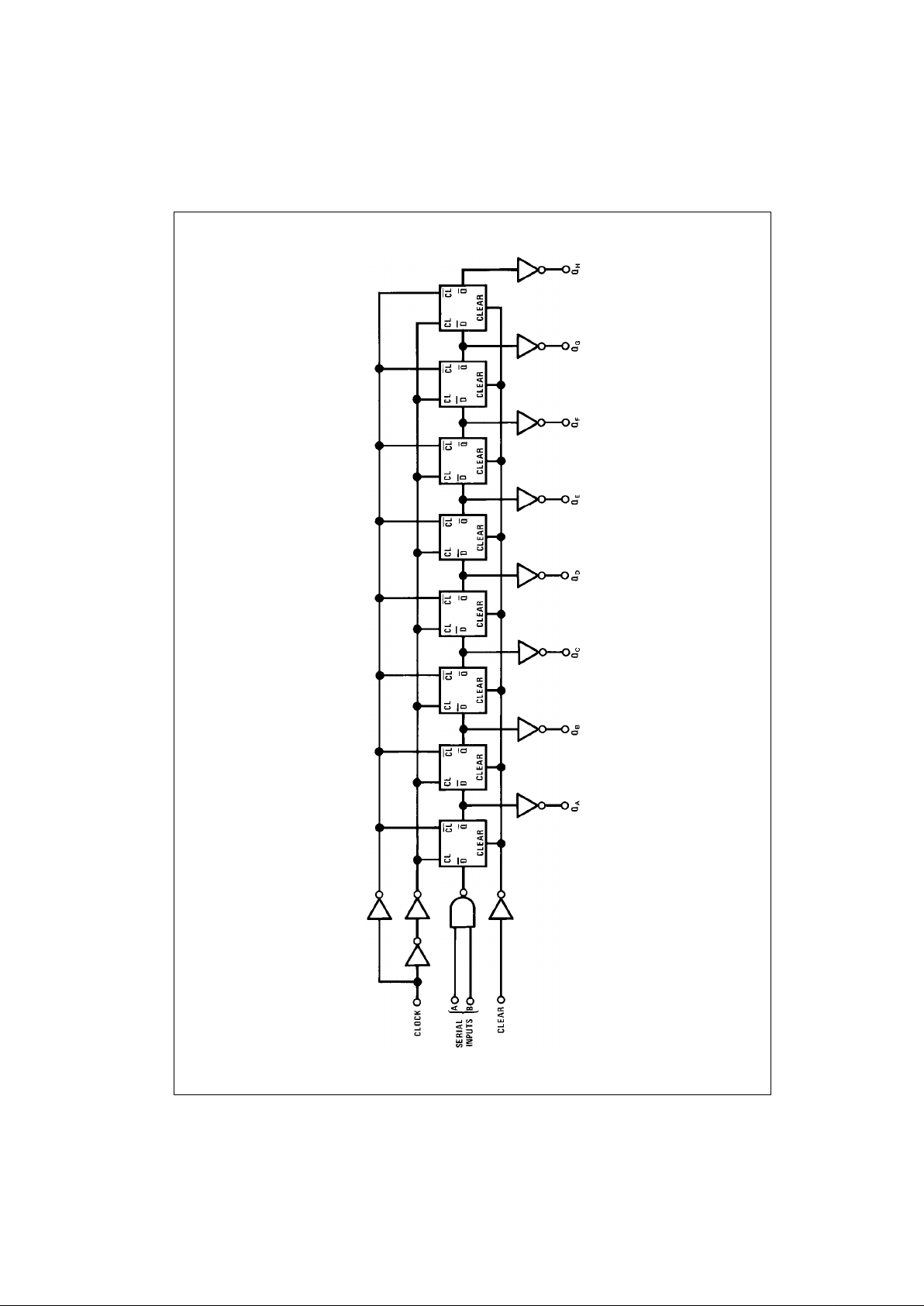
Block Diagram
Page 3
3 www.fairchildsemi.com
MM74C164
Absolute Maximum Ratings(Note 1)
Note 1: “Absolute Maximum Rat ings” are tho se values beyond which the
safety of the device cannot be guaranteed. E x c ept for “ Operating Temperature Range” they are not mea nt to imply that the devices sh ould be operated at these limits. The table of “Electrical Characteristics” provides
conditions for actual device o peration.
DC Electrical Characteristics
Min/Max limits apply across temperature range unless otherwise noted
Voltage at Any Pin −0.3V to VCC + 0.3V
Operating Temperature Range −40°C to +85°C
Storage Temperature Range −65°C to +150°C
Absolute Maximum V
CC
18V
Power Dissipation (P
D
)
Dual-In-Line 700 mW
Small Outline 500 mW
Operating V
CC
Range 3V to 15V
Lead Temperature
(soldering, 10 seconds) 260°C
Symbol Parameter Conditions Min Typ Max Units
CMOS TO CMOS
V
IN(1)
Logical “1” Input Voltage VCC = 5V 3.5 V
VCC = 10V 8.0 V
V
IN(0)
Logical “0” Input Voltage VCC = 5V 1.5 V
VCC = 10V 2.0 V
V
OUT(1)
Logical “1” Output Voltage VCC = 5V, IO = −10 µA4.5 V
VCC = 10V, IO = −10 µA9.0 V
V
OUT(0)
Logical “0” Output Voltage VCC = 5V, IO = +10 µA0.5V
VCC = 10V, IO = +10 µA1.0V
I
IN(1)
Logical “1” Input Current VCC = 15V, VIN = 15V 0.005 1.0 µA
I
IN(0)
Logical “0” Input Current VCC = 15V, VIN = 0V −1.0 −0.005 µA
I
CC
Supply Current VCC = 15V 0.05 300 µA
CMOS TO LPTTL INTERFACE
V
IN(1)
Logical “1” Input Voltage VCC = 4.75V VCC − 1.5 V
V
IN(0)
Logical “0” Input Voltage VCC = 4.75V 0.8 V
V
OUT(1)
Logical “1” Output Voltage VCC = 4.75V, IO = −360 µA2.4 V
V
OUT(0)
Logical “0” Output Voltage VCC = 4.75V, IO = 360 µA0.4V
OUTPUT DRIVE (See Family Characteristics Data Sheet) (Short Circuit Current)
I
SOURCE
Output Source Current VCC = 5V, V
IN(0)
= 0V −1.75 mA
TA = 25°C, V
OUT
= 0V
I
SOURCE
Output Source Current VCC = 10V, V
IN(0)
= 0V −8.0 mA
TA = 25°C, V
OUT
= 0V
I
SINK
Output Sink Current VCC = 5V, V
IN(1)
= 5V 1.75 mA
TA = 25°C, V
OUT
= V
CC
I
SINK
Output Sink Current VCC = 10V, V
IN(1)
= 10V 8.0 mA
TA = 25°C, V
OUT
= V
CC
Page 4

www.fairchildsemi.com 4
MM74C164
AC Electrical Charac teristics (Note 2)
TA = 25°C, CL = 50 pF, unless otherwise noted
Note 2: AC Parameters are guara nt eed by DC correlated testing.
Note 3: Capacitance is guaranteed by periodic testing.
Note 4: C
PD
determines the no load AC power consumption of any C M OS device. For complete explanation se e Family Characteristics applic ation note
AN-90.
Typical Applications
74C Compatibility
Guaranteed Noise Margin
as a Function of V
CC
Symbol Parameter Conditions Min Typ Max Units
t
pd1
Propagation Delay Time to a Logical “0” or a VCC = 5V 230 310 ns
Logical “1” from Clock to Q VCC = 10V 90 120 ns
t
pd0
Propagation Delay Time to a Logical “0” from VCC = 5V 280 380 ns
Clear to Q VCC = 10V 110 150 ns
t
S
Time Prior to Clock Pulse that Data VCC = 5V 200 110 ns
Must be Present VCC = 10V 80 30 ns
t
H
Time After Clock Pulse that VCC = 5V 0 0 ns
Data Must be Held VCC = 10V 0 0 ns
f
MAX
Maximum Clock Frequency VCC = 5V 2.0 3 MHz
VCC = 10V 5.5 8 MHz
t
W
Minimum Clear Pulse Width VCC = 5V 150 250 ns
VCC = 10V 55 90 ns
tr, t
f
Maximum Clock Rise and Fall Time VCC = 5V 15 µs
VCC = 10V 5 µs
C
IN
Input Capacitance Any Input (Note 3) 5 pF
C
PD
Power Dissipation Capacitance (Note 4) 140 pF
Page 5

5 www.fairchildsemi.com
MM74C164
Logic Waveform
AC Test Circuit
Switching Time Waveforms
CMOS to CMOS
tr = tf = 20 ns
TTL to CMOS
Page 6

www.fairchildsemi.com 6
MM74C164
Physical Dimensions inches (millimeters) unless otherwise noted
14-Lead Small Outline Integrated Circuit (SOIC), JEDEC MS-120, 0.150” Narrow
Package Number M14A
Page 7

Fairchild does not assume any responsibility for use of any circuitry described, no circuit patent licenses are impli ed and Fairchild reserves the right at any time without notice to change said circuitry and specifications.
MM74C164 8-Bit Parallel-Out Serial Shift Register
LIFE SUPPORT POLICY
FAIRCHILD’S PRODUCTS ARE NOT AUTHORIZED FOR USE AS CRITICAL COMPONENTS IN LIFE SUPPORT
DEVICES OR SYSTEMS WITHOUT THE EXPRESS WRITTEN APPROVAL OF THE PRESIDENT OF FAIRCHILD
SEMICONDUCTOR CORPORATION. As used herein:
1. Life support devices or systems are devices or syste ms
which, (a) are intended for surgical implant into the
body, or (b) support or sustain life, and (c) whose failure
to perform when properly used in accordance with
instructions for use provided in the labeling, can be reasonably expected to result in a significant injur y to the
user.
2. A critical component in any com ponent of a life support
device or system whose failure to p erform can be r easonably expected to cause the failure of the life suppor t
device or system, or to affect its safety or effectiveness.
www.fairchildsemi.com
Physical Dimensions inches (millimeters) unless otherwise noted (Continued)
14-Lead Plastic Dual-In-Line Package (PDIP), JEDEC MS-001, 0.300” Wide
Package Number N14A
 Loading...