

Page 1
MITSUMI
High Precision Operational Amplifier MM6558
High Precision Operational Amplifier
Monolithic IC MM6558 Series
Outline
This IC is a high precision operational amplifier, which is pin compatible with general use operational amplifier
4558, and has greatly improved input offset voltage and drift voltage. The offset is much smaller than for a
general use operational amplifier, so offset adjustment is not needed. This contributes to reduction in the
number of processes. Also, drift relative to stress is greatly reduced, so there is much less effect of stress due
to IC strain and the like.
Features
1. Low input offset voltage ±power supply 0.1mV typ. (MM6558, MM6559, MM6560, MM6561,
MM6572)
single power supply 0.2mV typ. (MM6564, MM6565)
2. Low input offset drift ±power supply ±1µV/°C typ. (MM6558, MM6559, MM6560, MM6561,
MM6572)
single power supply ±2µV/°C typ. (MM6564, MM6565)
3. Current consumption ±power supply 3.0mA typ. (MM6558, MM6559)
3.5mA typ. (MM6560, MM6572)
1.7mA typ. (MM6561)
single power supply 0.35mA typ. (MM6564)
0.35mA typ. (MM6565)
4. Through rate ±power supply 3V/µS (MM6558, MM6559, MM6560, MM6561)
6V/µS (MM6572)
single power supply 1V/µS (MM6564, MM6565)
5. Input conversion ±power supply 1.2µVrms (MM6558, MM6559, MM6560, MM6561)
interference voltage 0.5µVrms (MM6572)
single power supply 1.8µVrms (MM6564)
2.0µVrms (MM6565)
Package
1. SOP-8C, SOP-8E (MM65 F)
2. DIP-8B (MM65 D)
3. SIP-8A (MM65 S)
Applications
1. Office automation equipment
2. measurement equipment
3. sensor equipment
Page 2
MITSUMI
High Precision Operational Amplifier MM6558
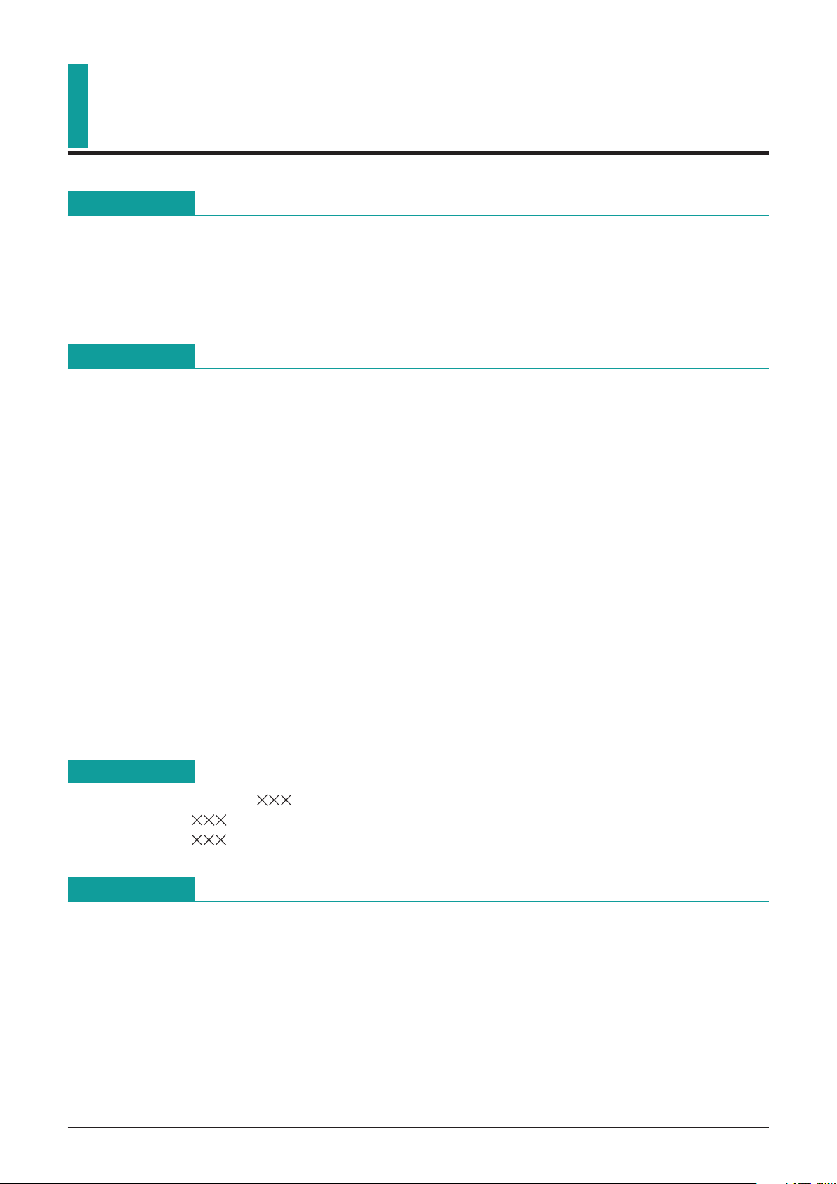
Absolute Maximum Ratings
(Ta=25°C)
Item Symbol Rating Units
Storage temperature T
STG
-
40~+125 °C
Operating temperature T
OPR
-
20~+75 °C
Power supply voltage V
+/V-
±12 V
Allowable power dissipation Pd 300 mW
Differential input voltage V
ID ±20 V
Input voltage V
I ±10 V
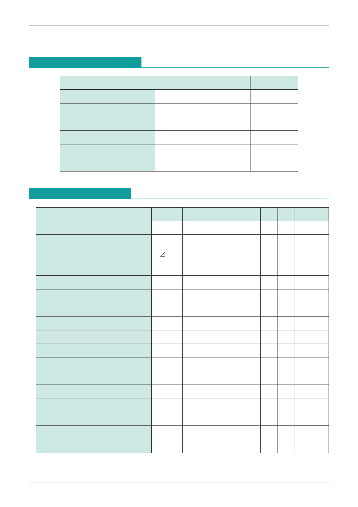
Electrical Characteristics
(Unless otherwise specified Ta=25°C, V+/V-=±10V)
Item Symbol Measurement Conditions Min. Typ. Max. Units
Operating power supply voltage range ±3.5 ±11 V
Input offset voltage V
IO RS
<
=
10kΩ 0.1 0.5 mV
Input offset voltage temperature drift V
IO ±1
µV/°C
Input offset current IIO 5 200 nA
Input bias current I
B 50 500 nA
Input resistance R
IN 0.3 3 MΩ
In-phase input voltage V
CM ±8 ±9 V
Voltage gain A
V RL
>
=
2kΩ, V
O=±7V 86 100 dB
Maximum output voltage V
O RL
>
=
10kΩ ±8 ±9 V
In-phase signal elimination ratio CMRR R
S
<
=
10kΩ 70 90 dB
Power supply voltage elimination ratio PSRR R
S
<
=
10kΩ 76.5 90 dB
Current consumption I
CC 3.0 5.0 mA
Output flow current I
SO 13 mA
Output inflow current I
SI 13 mA
Through rate SR R
L
>
=
2kΩ 3V/µS
Gain band area GBW 7 MHz
Input conversion interference voltage e
n RS=300Ω, IHFA (A curve) 1.2
µVrms
MM6558
Page 3

MITSUMI
High Precision Operational Amplifier MM6558
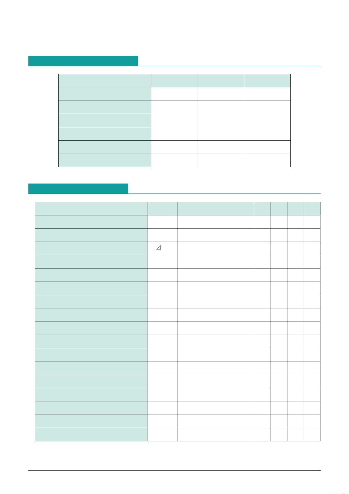
Absolute Maximum Ratings
(Ta=25°C)
Electrical Characteristics
(Unless otherwise specified Ta=25°C, V+/V-=±10V)
MM6559
Item Symbol Rating Units
Storage temperature T
STG
-
40~+125 °C
Operating temperature T
OPR
-
20~+75 °C
Power supply voltage V
+/V-
±12 V
Allowable power dissipation Pd 300 mW
Differential input voltage V
ID ±20 V
Input voltage V
I ±10 V
Item Symbol Measurement Conditions Min. Typ. Max. Units
Operating power supply voltage range ±2 ±11 V
Input offset voltage V
IO RS
<
=
10kΩ 0.1 0.5 mV
Input offset voltage temperature drift V
IO ±1
µV/°C
Input offset current IIO 5 200 nA
Input bias current I
B 50 500 nA
Input resistance R
IN 0.3 3 MΩ
In-phase input voltage V
CM ±8 ±9 V
Voltage gain A
V RL
>
=
2kΩ, V
O=±7V 86 100 dB
Maximum output voltage V
O RL
>
=
10kΩ ±8 ±9 V
In-phase signal elimination ratio CMRR R
S
<
=
10kΩ 70 90 dB
Power supply voltage elimination ratio PSRR R
S
<
=
10kΩ 76.5 90 dB
Current consumption I
CC 3.0 5.0 mA
Output flow current I
SO 13 mA
Output inflow current I
SI 13 mA
Through rate SR R
L
>
=
2kΩ 3V/µS
Gain band area GBW 7 MHz
Input conversion interference voltage e
n RS=300Ω, IHFA (Acurve) 1.2
µVrms
Page 4

MITSUMI
High Precision Operational Amplifier MM6558
Absolute Maximum Ratings
(Ta=25°C)
Electrical Characteristics
(Unless otherwise specified Ta=25°C, V+/V-=±10V)
MM6560
Item Symbol Rating Units
Storage temperature T
STG
-
40~+125 °C
Operating temperature T
OPR
-
20~+75 °C
Power supply voltage V
+/V-
±12 V
Allowable power dissipation Pd 300 mW
Differential input voltage V
ID ±20 V
Input voltage V
I ±10 V
Item Symbol Measurement Conditions Min. Typ. Max. Units
Operating power supply voltage range ±3.5 ±11 V
Input offset voltage V
IO RS
<
=
10kΩ 0.1 0.5 mV
Input offset voltage temperature drift V
IO ±1
µV/°C
Input offset current IIO 5 200 nA
Input bias current I
B 50 500 nA
Input resistance R
IN 0.3 3 MΩ
In-phase input voltage V
CM ±8 ±9 V
Voltage gain A
V RL
>
=
2kΩ, V
O=±7V 86 100 dB
Maximum output voltage V
O RL
>
=
2kΩ ±8 ±9 V
In-phase signal elimination ratio CMRR R
S
<
=
10kΩ 70 90 dB
Power supply voltage elimination ratio PSRR R
S
<
=
10kΩ 76.5 90 dB
Current consumption I
CC 3.5 5.7 mA
Output flow current I
SO 25 mA
Output inflow current I
SI 25 mA
Through rate SR R
L
>
=
2kΩ 3V/µS
Gain band area GBW 7 MHz
Input conversion interference voltage e
n RS=300Ω, IHFA (A curve) 1.2
µVrms
Page 5
MITSUMI
High Precision Operational Amplifier MM6558
Absolute Maximum Ratings
(Ta=25°C)
Electrical Characteristics
(Unless otherwise specified Ta=25°C, V+/V-=±10V)
MM6561
Item Symbol Rating Units
Storage temperature T
STG
-
40~+125 °C
Operating temperature T
OPR
-
20~+75 °C
Power supply voltage V
+/V-
±12 V
Allowable power dissipation Pd 300 mW
Differential input voltage V
ID ±20 V
Input voltage V
I ±10 V
Item Symbol Measurement Conditions Min. Typ. Max. Units
Operating power supply voltage range ±3.5 ±11 V
Input offset voltage V
IO RS
<
=
10kΩ 0.1 0.5 mV
Input offset voltage temperature drift V
IO ±1
µV/°C
Input offset current IIO 5 200 nA
Input bias current I
B 50 500 nA
Input resistance R
IN 0.3 3 MΩ
In-phase input voltage V
CM ±8 ±9 V
Voltage gain A
V RL
>
=
5kΩ, V
O=±7V 86 100 dB
Maximum output voltage V
O RL
>
=
10kΩ ±8 ±9 V
In-phase signal elimination ratio CMRR R
S
<
=
10kΩ 70 90 dB
Power supply voltage elimination ratio PSRR R
S
<
=
10kΩ 76.5 90 dB
Current consumption I
CC 1.7 2.7 mA
Output flow current I
SO 6mA
Output inflow current I
SI 6mA
Through rate SR R
L
>
=
2kΩ 3V/µS
Gain band area GBW 7 MHz
Input conversion interference voltage e
n RS=300Ω, IHFA (A curve) 1.2
µVrms
Page 6

MITSUMI
High Precision Operational Amplifier MM6558
Absolute Maximum Ratings
(Ta=25°C)
Electrical Characteristics
(Unless otherwise specified Ta=25°C, VCC=3V, V1=1V)
MM6564
Item Symbol Rating Units
Storage temperature T
STG
-
40~+125 °C
Operating temperature T
OPR
-
20~+75 °C
Power supply voltage V
CC max. 15 V
Allowable power dissipation Pd 300 mW
Input voltage V
I 0~15 V
Item Symbol Measurement Conditions Min. Typ. Max. Units
Operating power supply voltage range 2 3 13 V
Input offset voltage V
IO 0.2 0.9 mV
Input offset voltage temperature drift V
IO ±2
µV/°C
Input offset current IIO 530nA
Input bias current I
B 30 150 nA
Input voltage range V
I 0
VCC-
1
V
Voltage gain A
V RL
>
=
100kΩ 80 100 dB
Output voltage range V
O 0.1
VCC-
1
V
Output flow current I
SO 0.5 mA
In-phase signal elimination ratio CMRR R
S
<
=
10kΩ 70 90 dB
Power supply voltage elimination ratio PSRR R
S
<
=
10kΩ 76.5 90 dB
Current consumption I
CC 0.35 0.5 mA
Through rate SR 1 V/µS
Gain band area GBW 2 MHz
Input conversion interference voltage e
n RS=300Ω, IHFA (A curve) 1.8
µVrms
Page 7

MITSUMI
High Precision Operational Amplifier MM6558
Absolute Maximum Ratings
(Ta=25°C)
Electrical Characteristics
(Unless otherwise specified Ta=25°C, VCC=5V)
MM6565
Item Symbol Measurement Conditions Min. Typ. Max. Units
Operating power supply voltage range 4 5 13 V
Input offset voltage V
IO 0.2 0.9 mV
Input offset voltage temperature drift V
IO ±2
µV/°C
Input offset current IIO 530nA
Input bias current I
B 30 150 nA
Input voltage range V
I 0
VCC-
1
V
Voltage gain A
V RL
>
=
100kΩ 80 100 dB
Output voltage range V
O RL
>
=
10kΩ
GND+1
VCC-
1
V
Output flow current I
SO 0.5 mA
Output inflow current I
SI 0.5 mA
In-phase signal elimination ratio CMRR R
S
<
=
10kΩ 70 90 dB
Power supply voltage elimination ratio PSRR R
S
<
=
10kΩ 76.5 90 dB
Current consumption I
CC 0.35 0.5 mA
Through rate SR R
L
>
=
10kΩ 1V/µS
Gain band area GBW 1 MHz
Input conversion interference voltage e
n RS=300Ω, IHFA (A curve) 2.0
µVrms
Item Symbol Rating Units
Storage temperature T
STG
-
40~+125 °C
Operating temperature T
OPR
-
20~+75 °C
Power supply voltage V
CC max. 15 V
Allowable power dissipation Pd 300 mW
Input voltage V
I 0~15 V
Page 8

MITSUMI
High Precision Operational Amplifier MM6558
Absolute Maximum Ratings
(Ta=25°C)
Electrical Characteristics
(Unless otherwise specified Ta=25°C, V+/V-=±10V)
MM6572
Item Symbol Rating Units
Storage temperature T
STG
-
40~+125 °C
Operating temperature T
OPR
-
20~+75 °C
Power supply voltage V
+/V-
±12 V
Allowable power dissipation Pd 300 mW
Differential input voltage V
ID ±20 V
Input voltage V
I ±10 V
Item Symbol Measurement Conditions Min. Typ. Max. Units
Operating power supply voltage range ±2 ±11 V
Input offset voltage V
IO RS
<
=
10kΩ 0.1 0.5 mV
Input offset voltage temperature drift V
IO ±1
µV/°C
Input offset current IIO 10 100 nA
Input bias current I
B 200 500 nA
Input resistance R
IN 100 260 kΩ
In-phase input voltage V
CM ±8 ±9 V
Voltage gain A
V RL
>
=
2kΩ, V
O=±7V 86 100 dB
Maximum output voltage V
O RL
>
=
10kΩ ±8 ±9 V
In-phase signal elimination ratio CMRR R
S
<
=
10kΩ 70 90 dB
Power supply voltage elimination ratio PSRR R
S
<
=
10kΩ 76.5 90 dB
Current consumption I
CC 3.5 5.0 mA
Output flow current I
SO 13 mA
Output inflow current I
SI 13 mA
Through rate SR R
L
>
=
2kΩ 6V/µS
Gain band area GBW 10 MHz
Input conversion interference voltage e
n RS=300Ω, IHFA (A curve) 0.5
µVrms
Page 9

MITSUMI
High Precision Operational Amplifier MM6558
1 AOUT
2 AIN
-
3 AIN+
4 V
-
GND
5 B
IN+
6 BIN
-
7 BOUT
8 V+ VCC
Pin Assignment
8765
1234
24681012
-
0.5
-
0.4
-
0.3
-
0.2
-
0.1
0.1
0.2
0.3
0.4
0.5
Ta
=
25°C
Power supply voltage V+/V
-
( V)
0
Input offset voltage VIO (mV)
024681012
0
1
2
3
4
5
Ta
=
25°C
Power supply voltage V+/V
-
( V)
Consumption voltage ICC (mA)
10 100 1k 10k
1
10
Signal source resistance R
S (Ω)
Input conversion interference voltage
em (µVrms)
V+/V
-
=
10V, Ta
=
25°C
24681012
0
10
20
30
40
50
Input bias current IB
(nA)
Ta
=
25°C
Power supply voltage V+/V
-
( V)
Characteristics
MM6558
Pin Function
MM6558
MM6559
MM6564
Pin No..
MM6560
MM6565
MM6561
MM6572
Example of input calculation interference voltage relative
to signal source resistance characteristics
Example of input offset voltage relative to power supply
voltage characteristics
Example of input bias current relative to power supply
voltage characteristics
Example of current consumption relative to power
supply voltage characteristics
Page 10

MITSUMI
High Precision Operational Amplifier MM6558
0.1k 1k 10k
8
10
12
14
16
18
20
Load resistance RL (Ω)
V+/V
-
=
10V, Ta
=
25°C
Maximum output voltage amplitude
VOPP
(V)
-
12
-
8
-
4
0
4
8
12
24681012
Power supply voltage V+/V
-
( V)
RL
=
2kΩ, Ta=25°C
Maximum output voltage VO
(V)
1 10 100 1k 10k 100k 1M 10M
0
20
40
60
80
100
120
Frequency f (Hz)
V+/V
-
=
10V, R
L
=
2kΩ, Ta=25°C
voltage gain AV
(dB)
100 1k 10k 100k
0
20
40
60
80
100
120
Frequency f (Hz)
V+/V
-
=
9V, Ta
=
25°C
Power supply voltage elimination ratio
PSRR
(dB)
10 100 1k 10k 100k 1M
0
5
10
15
20
25
Frequency f (Hz)
V+/V
-
=
10V, RL
=
2kΩ, Ta=25°C
Maximum output voltage amplitude
VOPP
(V)
24681012
-
5
-
4
-
3
-
2
-
1
0
1
2
3
4
5
Power supply voltage V+/V
-
( V)
Ta
=
25°C
Input offset current IIO (nA)
0.01
0.1
1
10
Output voltage V
O (Vrms)
0.001
0.01
0.1
1
V+/V
-
=
6V, R
L
=
2kΩ, Ta=25°C
complete higher harmonic distortion rate
THD (%)
Example of input offset current to power supply voltage
characteristics
Example of complete higher harmonic distortion rate
output voltage characteristics
Example of power supply voltage elimination frequency
characteristics
Example of maximum output voltage amplitude frequency
characteristics
Example of maximum output voltage relative to power
supply voltage characteristics
Example of voltage gain frequency characteristics
Example of maximum output voltage amplitude relative to
load characteristics
Page 11

MITSUMI
High Precision Operational Amplifier MM6558
24681012
-
5
-
4
-
3
-
2
-
1
0
1
2
3
4
5
Ta
=
25°C
Power supply voltage V+/V
-
( V)
Input offset current IIO
(nA)
0.1k 1k 10k
8
10
12
14
16
18
20
Load resistance R
L (Ω)
V+/V
-
=
10V, Ta
=
25°C
Maximum output voltage amplitude
VOPP
(V)
2 4 6 8 10 12
-
0.5
-
0.4
-
0.3
-
0.2
-
0.1
0
0.1
0.2
0.3
0.4
0.5
Ta
=
25°C
Power supply voltage V+/V
-
( V)
Input offset voltage VIO
(mV)
024681012
0
1
2
3
4
5
Ta
=
25°C
Power supply voltage V+/V
-
( V)
Consumption current Icc
(mA)
24681012
-
5
-
4
-
3
-
2
-
1
0
1
2
3
4
5
Power supply voltage V+/V
-
( V)
Ta
=
25°C
Input offset current IIO
(nA)
24681012
-
0.5
-
0.4
-
0.3
-
0.2
-
0.1
0.1
0.2
0.3
0.4
0.5
Power supply voltage V+/V
-
( V)
Ta
=
25°C
0
Input offset voltage VIO
(mV)
024681012
0
1
2
3
4
5
Power supply voltage V+/V
-
( V)
Ta
=
25°C
Current consumption ICC
(mA)
MM6561
MM6559
Example of input offset voltage relative to power supply
voltage characteristics
Comparison of input offset current relative to power
supply voltage characteristics
Example of input offset voltage relative to power supply
voltage characteristics
Example of offset current relative to power supply voltage
characteristics
Example of current consumption relative to power supply
characteristics
Example of current consumption relative to power supply
voltage characteristics
Example of maximum output voltage amplitude relative to
load characteristics
Page 12

MITSUMI
High Precision Operational Amplifier MM6558
10 100 1k 10k
0
20
40
60
80
100
120
Frequency f (Hz)
V+/V
-
=
5V, Ta
=
25°C
Power supply voltage elimination ratio
PSRR
(dB)
10 100 1k 10k 100k 1M
0
5
10
15
20
25
Frequency f (Hz)
V+/V
-
=
6V, R
L
=
2kΩ, Ta=25°C
Maximum output voltage amplitude
VOPP
(V)
24681012
-
5
-
4
-
3
-
2
-
1
0
1
2
3
4
5
Ta
=
25°C
Power supply voltage V+/V
-
( V)
Input offset current IIO
(nA)
0.01
0.1
1
10
Output voltage V
O (Vrms)
V+/V
-
=
6V, R
L
=
2kΩ, Ta=25°C
0.001
0.01
0.1
1
complete higher harmonic distortion rate
THD (%)
24681012
-
0.5
-
0.4
-
0.3
-
0.2
-
0.1
0
0.1
0.2
0.3
0.4
0.5
Ta
=
25°C
Power supply voltage V+/V
-
( V)
Input offset voltage VIO (mV)
10 100 1k 10k
1
10
Signal source resistance Rs (Ω)
V+/V
-
=
6V, Ta
=
25°C
Input conversion interference voltage
en
(µVrms)
24681012
0
10
20
30
40
50
Ta
=
25°C
Power supply voltage V+/V
-
( V)
Input bias current IB
(nA)
MM6564
Example of input calculation interference voltage relative
to signal source resistance characteristics
Example of input offset voltage relative to power supply
voltage characteristics
Comparison of input offset current relative to power
supply voltage characteristics
Example of power supply voltage elimination
frequency characteristics
Example of input bias current relative to power supply
voltage characteristics
Example of complete higher harmonic distortion rate
output voltage characteristics
Example of maximum output voltage amplitude frequency
characteristics
2 4 6 8 10 12
-
12
-
8
-
4
0
4
8
12
Ta
=
25°C
Power supply voltage V+/V
-
( V)
Maximum output voltage
V
O
(V)
Example of maximum output voltage relative to power
supply voltage characteristics
Page 13

MITSUMI
High Precision Operational Amplifier MM6558
24681012
-
5
-
4
-
3
-
2
-
1
0
1
2
3
4
5
Ta
=
25°C
Power supply voltage V+/V
-
( V)
Input offset current
I
IO (nA)
10
0
20
40
60
80
100
120
100 1k 10k
Frequency f (Hz)
100k
V+/V
-
=
5V, Ta
=
25°C
Power supply voltage elimination ratio
PSRR
(dB)
24681012
-
0.5
-
0.4
-
0.3
-
0.2
-
0.1
0
0.1
0.2
0.3
0.4
0.5
Ta
=
25°C
Power supply voltage V+/V
-
( V)
Input offset voltag
V
IO (mV)
0.01
0.1
1
10
Output voltage V
O (Vrms)
0.001
0.01
0.1
1
V+/V
-
=
6V, R
L
=
2kΩ, Ta=25°C
Complete higher harmonic distortion rate
THD (%)
10 100 1k 10k
1
10
Signal source resistance Rs (Ω)
V+/V
-
=
6V, Ta
=
25°C
Input conversion interference voltage
en
(µVrms)
024681012
0.32
0.33
0.34
0.35
0.36
0.37
0.38
0.39
0.4
Ta
=
25°C
Power supply voltage V
CC (V)
Consumption voltage
I
CC
(mA)
1 10 100 1k 10k 100k 1M 10M
0
20
40
60
80
100
120
Frequency f (Hz)
V+/V
-
=
6V, Ta
=
25°C
Voltage gain AV
(dB)
MM6565
Example of input calculation interference voltage relative
to signal source resistance characteristics
Example of input offset voltage relative to power supply
voltage characteristics
Example of input offset current to power supply
voltage characteristics
Example of voltage gain frequency characteristics
Example of current consumption relative to power
supply voltage characteristics
Example of complete higher harmonic distortion rate
output voltage characteristics
Example of power supply voltage elimination frequency
characteristics
Page 14

MITSUMI
High Precision Operational Amplifier MM6558
1k 10k 100k
5
6
7
8
9
10
11
12
13
14
15
Load resistance R
L (Ω)
V+/V
-
=
7.5V, Ta
=
25°C
Maximum output voltage amplitude
VOPP
(V)
1 10 100 1k 10k 100k 1M 10M
0
20
40
60
80
100
120
V+/V
-
=
6V, R
L
=
2kΩ, Ta=25°C
Voltage gain AV
(dB)
24681012
-
12
-
8
-
4
0
4
8
12
Ta
=
25°C
Power supply voltage V+/V
-
( V)
Maximum output voltage
V
O
(V)
10 100 1k 10k 100k 1M
0
5
10
15
20
25
Frequency f (Hz)
V+/V
-
=
6V, RL
=
2kΩ, Ta=25°C
Maximum output voltage amplitude
VOPP
(V)
Example of maximum output voltage relative to power
supply voltage characteristics
Example of maximum output voltage amplitude relative to
load characteristics
Example of maximum output voltage amplitude
frequency characteristics
Example of voltage gain frequency characteristics
 Loading...