

Page 1
MM58342 High Voltage Display Driver
MM58342 High Voltage Display Driver
February 1995
General Description
The MM58342 is a monolithic MOS integrated circuit utilizing CMOS metal gate low threshold P- and N-channel devices. It is available both in 28-pin molded dual-in-line packages or as dice. The MM58342 is particularly suited for driving high voltage (35V max) vacuum fluorescent (VF) displays (e.g., a 20-digit alphanumeric or dot matrix display).
Applications
Y
COPSTMor microprocessor-driven displays
Y
Instrumentation readouts
Y
Industrial control indicator
Y
Digital clock, thermostat, counter, voltmeter
Y
Word processor text displays
Y
Automotive dashboards
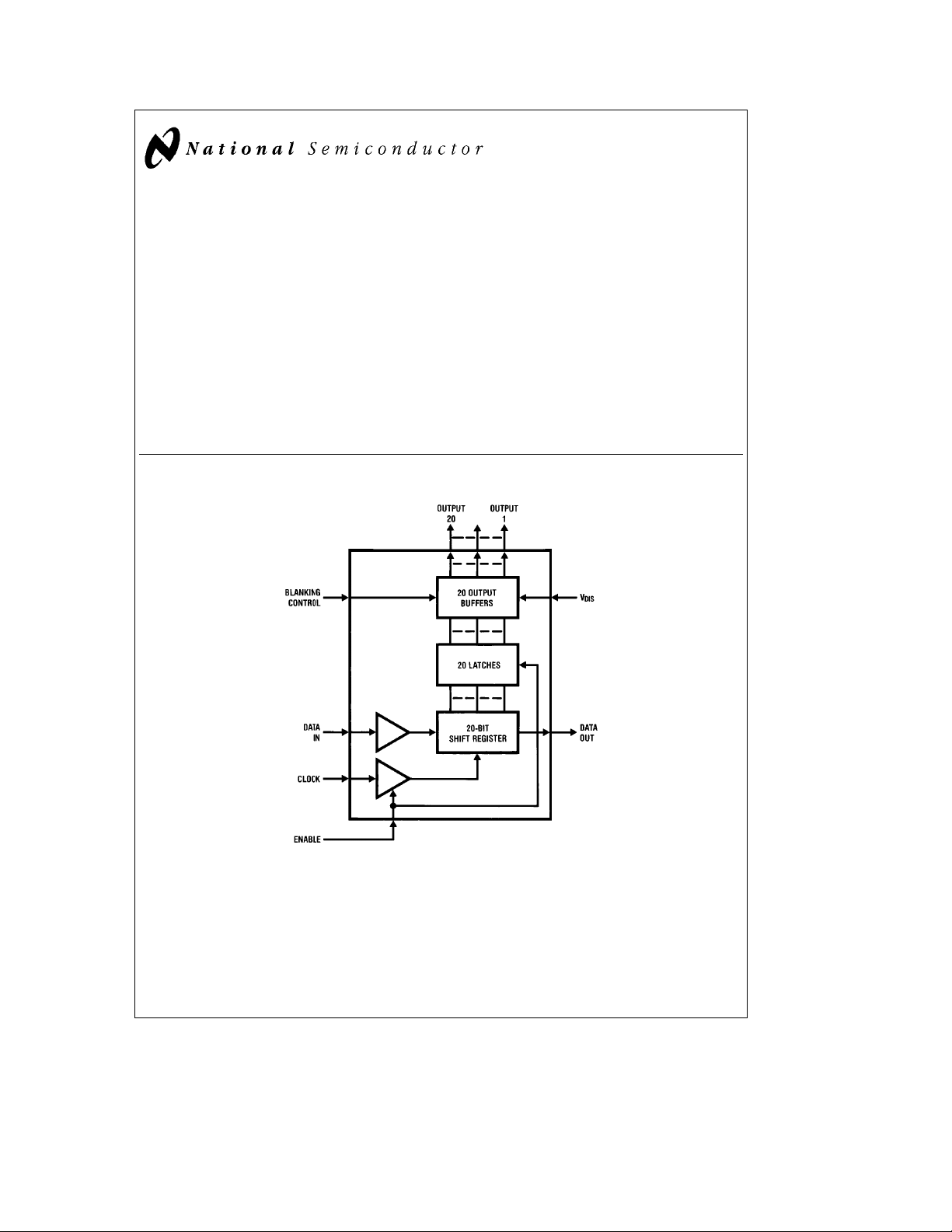
Block Diagram
Features
Y
Direct interface to high voltage display
Y
Serial data input
Y
No external resistors required
Y
Wide display power supply operation
Y
LSTTL compatible inputs
Y
Software compatible with NS display driver family
Y
Compatible with alphanumeric or dot matrix displays
Y
Display blanking control input
Y
Simple to cascade
FIGURE 1
TL/F/7925– 1
COPSTMis a trademark of National Semiconductor Corporation.
C
1995 National Semiconductor Corporation RRD-B30M105/Printed in U. S. A.
TL/F/7925
Page 2
Absolute Maximum Ratings
If Military/Aerospace specified devices are required,
please contact the National Semiconductor Sales
Office/Distributors for availability and specifications.
Voltage at Any Input Pin V
Voltage at Any Display Pin VDDto V
a
V
V
l
DIS
l
DD
Storage Temperature
DD
a
0.3V to V
SS
DD
b
65§Ctoa150§C
b
b
36.5V
36.5V
0.3V
Operating Conditions
Supply Voltage (V
e
V
0V 4.5 5.5 V
SS
Display Voltage (V
Temperature Range
DD
DIS
Min Max Units
)
b
)
30
b
40
b
10 V
a
85
C
§
Power Dissipation at 25§C
Molded DIP Package, Board Mount 2.03W*
Molded DIP Package, Socket Mount 1.83W**
Junction Temperature 130
C
§
Lead Temperature (Soldering, 10 sec.) 260§C
*Molded DIP Package, Board Mount, i
derate 19.2 mW/
C above 25§C.
§
**Molded DIP Package, Socket Mount, i
derate 17.2 mW/
C above 25§C.
§
JA
JA
e
52§C/W,
e
58§C/W,
DC Electrical Characteristics
eb
T
40§Ctoa85§C, V
A
Symbol Parameter Conditions Min Typ Max Units
Power Supply Currents
I
DD
I
DIS
Input Logic Levels
DATA IN, CLOCK
ENABLE, BLANK
V
IL
V
IH
Logic ‘0’ 0.8 V
Logic ‘1’ (Note 1) 2.4 V
Data Output Logic Levels
V
OL
V
OH
V
OH
I
IN
C
IN
Logic ‘0’ I
Logic ‘1’ I
Logic ‘1’ I
Input Currents DATA IN, V
CLOCK ENABLE, BLANK
Input Capacitance DATA IN,
CLOCK ENABLE, BLANK
Display Output Impedances V
R
OFF
R
ON
V
DOL
Note 1: 74LSTTL V
Output Off
Output On
Display Output Low Voltage V
e
OH
DD
(Figure 3a)
(Figure 3b)
2.7V@I
OUT
e
5Vg0.5V, V
eb
400 mA, TTL V
e
0V unless otherwise specified
SS
e
V
VSSor VDD,V
IN
V
Disconnected
DIS
e
V
5.5V, V
DD
All Outputs Low
e
400 mA 0.4 V
OUT
eb
OUT
OUT
V
V
V
V
V
V
b
10 mAV
eb
500 mA 2.8 V
e
0V or V
IN
DD
DIS
DIS
DIS
DIS
DIS
DIS
DD
30VsV
OH
DD
e
5.5V, V
eb
10V 55 250 kX
eb
20V 60 300 kX
eb
30V 65 400 kX
eb
10V 700 800 X
eb
20V 600 750 X
eb
30V 500 680 X
e
5.5V, I
OUT
DIS
e
2.4V@I
SS
SS
s
b
OUT
e
SS
e
0V, V
e
0V
e
Open Circuit,
10V
eb
400 mA.
DIS
0V,
eb
30V
b
0.5 V
DD
b
10 10 mA
V
DIS
150 mA
10 mA
15 pF
a
V
2V
DIS
2
Page 3

AC Electrical Characteristics T
eb
40§Ctoa85§C, V
A
DD
e
5Vg0.5V
Symbol Parameter Conditions Min Typ Max Units
Clock Input (Notes 3 and 4)
f
C
t
H
t
L
Frequency 800 kHz
High Time 300 ns
Low Time 300 ns
Data Input
t
DS
t
DH
Set-Up Time 100 ns
Hold Time 100 ns
Enable Input (Note 2)
t
ES
t
EH
t
CDO
Note 2: For timing purposes, the signals ENABLE and BLANK can be considered to be totally independent of each other.
Note 3: AC input waveform specification for test purposes: t
Note 4: Clock input rise and fall times must not exceed 5 ms.
Set-Up Time 100 ns
Hold Time 100 ns
Data Output C
CLOCK Low to Data Out 500 ns
e
50 pF
L
Time
s
20 ns, fe800 kHz, 50%g10% duty cycle.
r,tf
Connection Diagrams
Dual-In-Line Package
Plastic Chip Carrier
Top View
TL/F/7925– 2
FIGURE 2
Order Number MM58342N
See NS Package Number N28B
Functional Description
This product is specifically designed to drive multiplexed or
non-multiplexed high voltage alphanumeric or dot matrix
vacuum fluorescent (VF) displays. Character generation is
done externally in the microprocessor, with a serial data
path to the display driver. The MM58342 uses three signals,
DATA IN, CLOCK and ENABLE, where ENABLE acts as an
external load signal. Display blanking can be achieved by
means of the BLANKING CONTROL input, and a logic ‘1’
will turn off all sections of the display. A block diagram of
the MM58342 is shown in
Figure 1
.
Top View
Order Number MM58342V
See NS Package Number V28A
Figure 2
shows the pinout of the MM58342 device, where
output 1 (pin 12) is equivalent to bit 1 (i.e., the first bit of data
to be loaded into the shift register following ENABLE high).
A logic ‘1’ at the input will turn on the corresponding display
digit/segment/dot output.
A significant reduction in discrete board components can be
achieved by use of the MM58342, because external pulldown resistors are not required. Due to the nature of the
output stage, both its on and off impedance values vary as a
function of the display voltage applied. However,
3
TL/F/7925– 8
Figures 3a
Page 4

Functional Description (Continued)
3b
show that this output impedance will remain con-
and
stant for a fixed value of display voltage.
Figure 4
demonstrates the critical timing requirements be-
tween CLOCK and DATA IN for the MM58342.
To clear (reset) the display driver at power on or any time,
the following flushing routine may be used. With the enable
signal high, clock in 20 zeroes. Drive the enable signal low
and the display will be blank. It is recommended to clear the
driver at power on.
In
Figure 5
only while this signal is at a logic ‘1’ does the circuit accept
CLOCK input signals. Data is transferred and shifted in the
internal shift register on the rising clock edge, i.e., ‘0’ –‘1’
transition. When the ENABLE signal goes low, the contents
, the ENABLE signal acts as an envelope, and
of the shift registers are latched, and the display will show
new data. During data transfer, the display will show old
data. DATA OUT is also provided on the MM58342 being
output on the falling edge. At any time, the display may be
blanked under processor control, using the BLANKING
CONTROL input.
Figure 6
shows a schematic diagram of a microprocessorbased system where the MM58342 is used to provide the
grid drive for a 40-digit 2 line5x7multiplexed vacuum
fluorescent (VF) display. The anode drive in this example is
provided by another member of the high voltage display
driver family, namely the MM58348, which does not require
an externally generated load signal.
Timing Diagrams
FIGURE 3a. Output Impedance Off
FIGURE 3b. Output Impedance On
For the purposes of AC measurement, V
FIGURE 4. Clock and Data Timings
TL/F/7925– 3
TL/F/7925– 4
e
IH
2.4V, V
e
0.8V.
IL
TL/F/7925– 5
4
Page 5

Timing Diagrams (Continued)
Typical Application
FIGURE 5. Timings (Data Format)
TL/F/7925– 6
TL/F/7925– 7
FIGURE 6. Microprocessor-Controlled Word Processor
5
Page 6

Physical Dimensions inches (millimeters)
MM58342 High Voltage Display Driver
Molded Dual-In-Line Package (N)
Order Number MM58342N
NS Package Number N28B
Plastic Chip Carrier (V)
Order Number MM58342V
NS Package Number V28A
LIFE SUPPORT POLICY
NATIONAL’S PRODUCTS ARE NOT AUTHORIZED FOR USE AS CRITICAL COMPONENTS IN LIFE SUPPORT
DEVICES OR SYSTEMS WITHOUT THE EXPRESS WRITTEN APPROVAL OF THE PRESIDENT OF NATIONAL
SEMICONDUCTOR CORPORATION. As used herein:
1. Life support devices or systems are devices or 2. A critical component is any component of a life
systems which, (a) are intended for surgical implant support device or system whose failure to perform can
into the body, or (b) support or sustain life, and whose be reasonably expected to cause the failure of the life
failure to perform, when properly used in accordance support device or system, or to affect its safety or
with instructions for use provided in the labeling, can effectiveness.
be reasonably expected to result in a significant injury
to the user.
National Semiconductor National Semiconductor National Semiconductor National Semiconductor
Corporation Europe Hong Kong Ltd. Japan Ltd.
1111 West Bardin Road Fax: (
Arlington, TX 76017 Email: cnjwge@tevm2.nsc.com Ocean Centre, 5 Canton Rd. Fax: 81-043-299-2408
Tel: 1(800) 272-9959 Deutsch Tel: (
Fax: 1(800) 737-7018 English Tel: (
National does not assume any responsibility for use of any circuitry described, no circuit patent licenses are implied and National reserves the right at any time without notice to change said circuitry and specifications.
Fran3ais Tel: (
Italiano Tel: (
a
49) 0-180-530 85 86 13th Floor, Straight Block, Tel: 81-043-299-2309
a
49) 0-180-530 85 85 Tsimshatsui, Kowloon
a
49) 0-180-532 78 32 Hong Kong
a
49) 0-180-532 93 58 Tel: (852) 2737-1600
a
49) 0-180-534 16 80 Fax: (852) 2736-9960
 Loading...