

Page 1
TL/F/11219
MM58274C Microprocessor Compatible Real Time Clock
April 1991
MM58274C
Microprocessor Compatible Real Time Clock
General Description
The MM58274C is fabricated using low threshold metal gate
CMOS technology and is designed to operate in bus oriented microprocessor systems where a real time clock and calendar function are required. The on-chip 32.768 kHz crystal
controlled oscillator will maintain timekeeping down to 2.2V
to allow low power standby battery operation. This device is
pin compatible with the MM58174A but continues timekeeping up to tens of years. The MM58274C is a direct replacement for the MM58274 offering improved Bus access cycle
times.
Applications
Y
Point of sale terminals
Y
Teller terminals
Y
Word processors
Y
Data logging
Y
Industrial process control
Features
Y
Same pin-out as MM58174A, MM58274B, and
MM58274
Y
Timekeeping from tenths of seconds to tens of years in
independently accessible registers
Y
Leap year register
Y
Hours counter programmable for 12 or 24-hour
operation
Y
Buffered crystal frequency output in test mode for easy
oscillator setting
Y
Data-changed flag allows simple testing for time
rollover
Y
Independent interrupting time with open drain output
Y
Fully TTL compatible
Y
Low power standby operation (10 mA at 2.2V)
Y
Low cost 16-pin DIP and 20-pin PCC
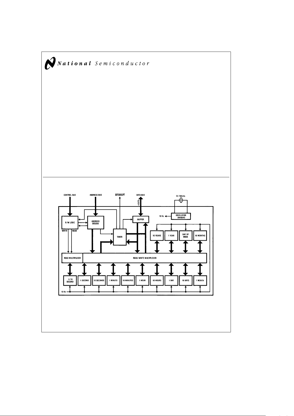
Block Diagram
TL/F/11219– 1
FIGURE 1
TRI-STATEÉis a registered trademark of National Semiconductor Corp.
Microbus
TM
is a trademark of National Semiconductor Corp.
C
1995 National Semiconductor Corporation RRD-B30M105/Printed in U. S. A.
Page 2
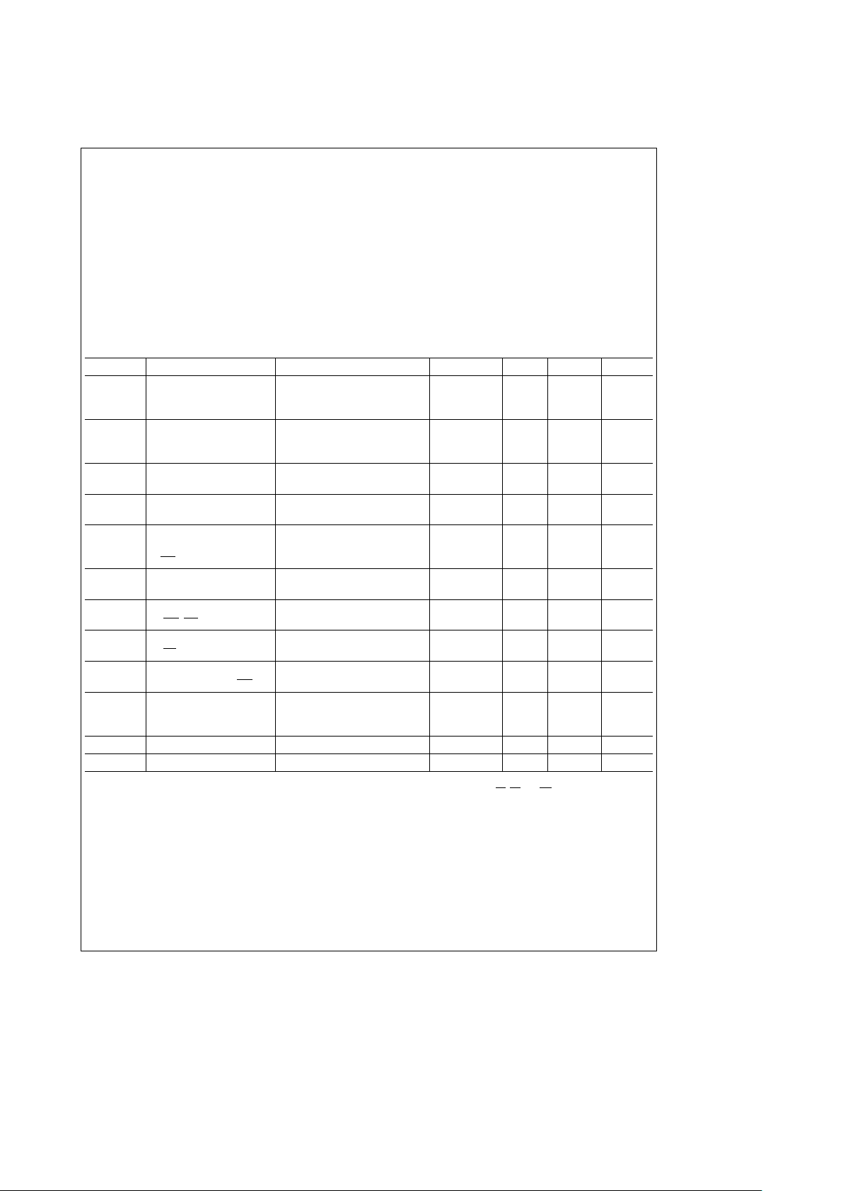
Absolute Maximum Ratings (Note 1)
If Military/Aerospace specified devices are required,
please contact the National Semiconductor Sales
Office/Distributors for availability and specifications.
DC Input or Output Voltage
b
0.3V to V
DD
a
0.3V
DC Input or Output Diode Current
g
5.0 mA
Storage Temperature, T
STG
b
65§Ctoa150§C
Supply Voltage, V
DD
6.5V
Power Dissipation, P
D
500 mW
Lead Temperature
(Soldering, 10 seconds) 260
§
Operating Conditions
Min Max Units
Operating Supply Voltage 4.5 5.5 V
Standby Mode Supply Voltage 2.2 5.5 V
DC Input or Output Voltage 0 V
DD
V
Operating Temperature Range
b
40 85
§
C
Electrical Characteristics V
DD
e
5Vg10%, Teb40§Ctoa85§C unless otherwise stated.
Symbol Parameter Conditions Min Typ Max Units
V
IH
High Level Input 2.0 V
Voltage (except
XTAL IN)
V
IL
Low Level Input 0.8 V
Voltage (except
XTAL IN)
V
OH
High Level Output I
OH
eb
20 mAV
DD
b
0.1 V
Voltage (DB0–DB3) I
OH
eb
1.6 mA 3.7 V
V
OH
High Level Output I
OH
eb
20 mAV
DD
b
0.1 V
Voltage (INT) (In Test Mode)
V
OL
Low Level Output I
OL
e
20 mA 0.1 V
Voltage (DB0–DB3, i
OL
e
1.6 mA 0.4 V
INT)
I
IL
Low Level Input Current V
IN
e
VSS(Note 2)
b
5
b
80 mA
(AD0–AD3, DB0 –DB3)
I
IL
Low Level Input Current V
IN
e
VSS(Note 2)
b
5
b
190 mA
(WR
,RD)
I
IL
Low Level Input Current V
IN
e
VSS(Note 2)
b
5
b
550 mA
(CS)
I
OZH
Ouput High Level V
OUT
e
V
DD
2.0 mA
Leakage Current (INT
)
I
DD
Average Supply Current All V
IN
e
VCCor Open Circuit
V
DD
e
2.2V (Standby Mode) 4 10 mA
V
DD
e
5.0V (Active Mode) 1 mA
C
IN
Input Capacitance 5 10 pF
C
OUT
Output Capacitance (Outputs Disabled) 10 pF
Note 1: Absolute Maximum Ratings are those values beyond which damage to the device may occur. All voltages referenced to ground unless otherwise noted.
Note 2: The DB0 –DB3 and AD0 –AD3 lines all have active P-channel pull-up transistors which will source current. The CS
,RD, and WR lines have internal pull-up
resistors to V
DD
.
2
Page 3
AC Switching Characteristics
READ TIMING: DATA FROM PERIPHERAL TO MICROPROCESSOR V
DD
e
5Vg0.5V, C
L
e
100 pF
Commercial
Symbol Parameter
Specification
Units
T
A
eb
40§Ctoa85§C
Min Typ Max
t
AD
Address Bus Valid to Data Valid 390 650 ns
t
CSD
Chip Select On to Data Valid 140 300 ns
t
RD
Read Strobe On to Data Valid 140 300 ns
t
RW
Read Strobe Width (Note 3, Note 7) DC
t
RA
Address Bus Hold Time from Trailing Edge 0 ns
of Read Strobe
t
CSH
Chip Select Hold Time from Trailing Edge 0 ns
of Read Strobe
t
RH
Data Hold Time from Trailing Edge 70 160 ns
of Read Strobe
t
HZ
Time from Trailing Edge of Read Strobe 250 ns
Until O/P Drivers are TRI-STATE
É
WRITE TIMING: DATA FROM MICROPROCESSOR TO PERIPHERAL V
DD
e
5Vg0.5V
Commercial
Symbol Parameter
Specification
Units
T
A
eb
40§Ctoa85§C
Min Typ Max
t
AW
Address Bus Valid to Write Strobe O 400 125 ns
(Note 4, Note 6)
t
CSW
Chip Select On to Write Strobe O 250 100 ns
t
DW
Data Bus Valid to Write Strobe O 400 220 ns
t
WW
Write Strobe Width (Note 6) 250 95 ns
t
WCS
Chip Select Hold Time Following 0 ns
Write Strobe O
t
WA
Address Bus Hold Time Following 0 ns
Write Strobe O
t
WD
Data Bus Hold Time Following 100 35 ns
Write Strobe O
t
AWS
Address Bus Valid Before 70 20 ns
Start of Write Strobe
Note 3: Except for special case restriction: with interrupts programmed, max read strobe width of control register (ADDR 0) is 30 ms. See section on Interrupt
Programming.
Note 4: All timings measured to the trailing edge of write strobe (data latched by the trailing edge of WR
).
Note 5: Input test waveform peak voltages are 2.4V and 0.4V. Output signals are measured to their 2.4V and 0.4V levels.
Note 6: Write strobe as used in the Write Timing Table is defined as the period when both chip select and write inputs are low, ie., WS
,eCSaWR. Hence write
strobe commences when both signals are low, and terminates when the first signal returns high.
Note 7: Read strobe as used in the Read Timing Table is defined as the period when both chip select and read inputs are low, ie., RS
eCSa
RD.
Note 8: Typical numbers are at V
CC
e
5.0V and T
A
e
25§C.
3
Page 4
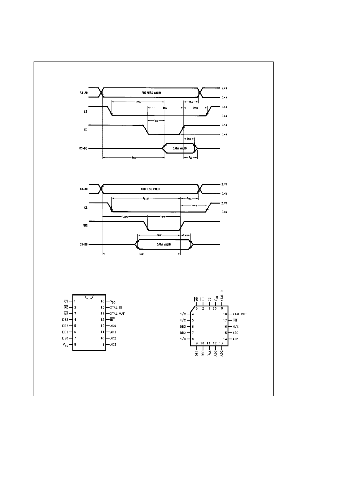
Switching Time Waveforms
Read Cycle Timing (Notes 5 and 7)
TL/F/11219– 2
Write Cycle Timing (Notes 5 and 6)
TL/F/11219– 3
Connection Diagrams
Dual-In-Line Package
TL/F/11219– 4
Top View
PCC Package
TL/F/11219– 5
Top View
FIGURE 2
Order Number MM58274CJ, MM58274CN or MM58274CV
See NS Package J16A, N16A, or V20A
4
Page 5
Functional Description
The MM58274C is a bus oriented microprocessor real time
clock. It has the same pin-out as the MM58174A while offering extended timekeeping up to units and tens of years. To
enhance the device further, a number of other features have
been added including: 12 or 24 hours counting, a testable
data-changed flag giving easy error-free time reading and
simplified interrupt control.
A buffered oscillator signal appears on the interrupt output
when the device is in test mode. This allows for easy oscillator setting when the device is initially powered up in a system.
The counters are arranged as 4-bit words and can be randomly accessed for time reading and setting. The counters
output in BCD (binary coded decimal) 4-bit numbers. Any
register which has less than 4 bits (e.g., days of week uses
only 3 bits) will return a logic 0 on any unused bits. When
written to, the unused inputs will be ignored.
Writing a logic 1 to the clock start/stop control bit resets the
internal oscillator divider chain and the tenths of seconds
counter. Writing a logic 0 will start the clock timing from the
nearest second. The time then updates every 100 ms with
all counters changing synchronously. Time changing during
a read is detected by testing the data-changed bit of the
control register after completing a string of clock register
reads.
Interrupt delay times of 0.1s, 0.5s, 1s, 5s, 10s, 30s or 60s
can be selected with single or repeated interrupt outputs.
The open drain output is pulled low whenever the interrupt
timer times out and is cleared by reading the control register.
CIRCUIT DESCRIPTION
The block diagram in
Figure 1
shows the internal structure
of the chip. The 16-pin package outline is shown in
Figure 2
.
Crystal Oscillator
This consists of a CMOS inverter/amplifier with an on-chip
bias resistor. Externally a 20 pF capacitor,a6pF–36pF
trimmer capacitor and a crystal are suggested to complete
the 32.768 kHz timekeeping oscillator circuit.
The 6 pF –36 pF trimmer fine tunes the crystal load impedance, optimizing the oscillator stability. When properly adjusted (i.e., to the crystal frequency of 32.768 kHz), the circuit will display a frequency variation with voltage of less
than 3 ppm/V. When an external oscillator is used, connect
to oscillator input and float (no connection) the oscillator
output.
When the chip is enabled into test mode, the oscillator is
gated onto the interrupt output pin giving a buffered oscillator output that can be used to set the crystal frequency
when the device is installed in a system. For further information see the section on Test Mode.
Divider Chain
The crystal oscillator is divided down in three stages to produce a 10 Hz frequency setting pulse. The first stage is a
non-integer divider which reduces the 32.768 kHz input to
30.720 kHz. This is further divided by a 9-stage binary ripple
counter giving an output frequency of 60 Hz. A 3-stage
Johnson counter divides this by six, generating a 10 Hz output. The 10 Hz clock is gated with the 32.768 kHz crystal
frequency to provide clock setting pulses of 15.26 ms duration. The setting pulse drives all the time registers on the
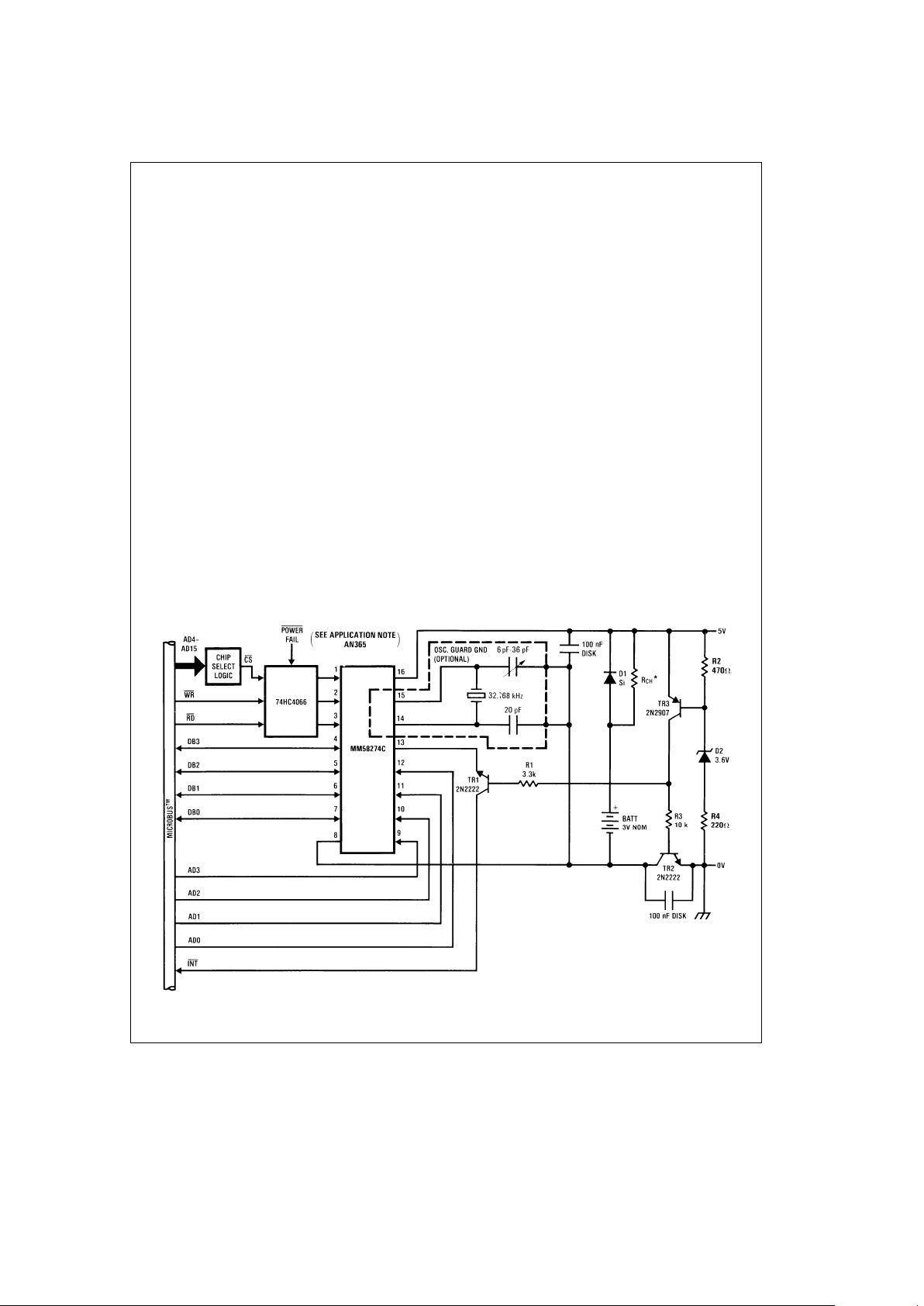
*Use resistor with Ni-cad cells only
TL/F/11219– 6
FIGURE 3. Typical System Connection Diagram
5
Page 6

Functional Description (Continued)
device which are synchronously clocked by this signal. All
time data and data-changed flag change on the falling edge
of the clock setting pulse.
Data-Changed Flag
The data-changed flag is set by the clock setting pulse to
indicate that the time data has been altered since the clock
was last read. This flag occupies bit 3 of the control register
where it can be tested by the processor to sense datachanged. It will be reset by a read of the control register.
See the section, ‘‘Methods of Device Operation’’, for suggested clock reading techniques using this flag.
Seconds Counters
There are three counters for seconds:
a) tenths of seconds
b) units of seconds
c) tens of seconds.
The registers are accessed at the addresses shown in Table I. The tenths of seconds register is reset to 0 when the
clock start/stop bit (bit 2 of the control register) is set to
logic 1. The units and tens of seconds are set up by the
processor, giving time setting to the nearest second. All
three registers can be read by the processor for time output.
Minutes Counters
There are two minutes counters:
a) units of minutes
b) tens of minutes.
Both registers may be read to or written from as required.
Hours Counters
There are two hours counters:
a) units of hours
b) tens of hours.
Both counters may be accessed for read or write operations
as desired.
In 12-hour mode, the tens of hours register has only one
active bit and the top three bits are set to logic 0. Data bit 1
of the clock setting register is the AM/PM indicator; logic 0
indicating AM, logic 1 for PM.
When 24-hour mode is programmed, the tens of hours register reads out two bits of data and the two most significant
bits are set to logic 0. There is no AM/PM indication and bit
1 of the clock setting register will read out a logic 0.
In both 12/24-hour modes, the units of hours will read out
four active data bits. 12 or 24-hour mode is selected by bit 0
of the clock setting register, logic 0 for 12-hour mode, logic
1 for the 24-hour mode.
Days Counters
There are two days counters:
a) units of days
b) tens of days.
The days counters will count up to 28, 29, 30 or 31 depending on the state of the months counters and the leap year
counter. The microprocessor has full read/write access to
these registers.
Months Counters
There are two months counters:
a) units of months
b) tens of months.
Both these counters have full read/write access.
Years Counters
There are two years counters:
a) units of years
b) tens of years.
Both these counters have full read/write access. The years
will count up to 99 and roll over to 00.
TABLE I. Address Decoding of Real-Time Clock Internal Registers
Register Selected
Address (Binary)
(Hex) Access
AD3 AD2 AD1 AD0
0 Control Register 0 0 0 0 0 Split Read and Write
1 Tenths of Seconds 0 0 0 1 1 Read Only
2 Units Seconds 0 0 1 0 2 R/W
3 Tens Seconds 0 0 1 1 3 R/W
4 Units Minutes 0 1 0 0 4 R/W
5 Tens Minutes 0 1 0 1 5 R/W
6 Unit Hours 0 1 1 0 6 R/W
7 Tens Hours 0 1 1 1 7 R/W
8 Units Days 1 0 0 0 8 R/W
9 Tens Days 1 0 0 1 9 R/W
10 Units Months 1 0 1 0 A R/W
11 Tens Months 1 0 1 1 B R/W
12 Units Years 1 1 0 0 C R/W
13 Tens Years 1 1 0 1 D R/W
14 Day of Week 1 1 1 0 E R/W
15 Clock Setting/ 1 1 1 1 F R/W
Interrupt Registers
6
Page 7

Functional Description (Continued)
Day of Week Counter
The day of week counter increments as the time rolls from
23:59 to 00:00 (11:59 PM to 12:00 AM in 12-hour mode). It
counts from 1 to 7 and rolls back to 1. Any day of the week
may be specified as day 1.
Clock Setting Register/Interrupt Register
The interrupt select bit in the control register determines
which of these two registers is accessible to the processor
at address 15. Normal clock and interrupt timing operations
will always continue regardless of which register is selected
onto the bus. The layout of these registers is shown in
Table II.
The clock setting register is comprised of three separate
functions:
a) leap year counter: bits 2 and 3
b) AM/PM indicator: bit 1
c) 12-hour mode set: bit 0 (see Table IIA).
The leap year counter is a 2-stage binary counter which
is clocked by the months counter. It changes state as the
time rolls over from 11:59 on December 31 to 00:00 on
January 1.
The counter should be loaded with the ‘number of years
since last leap year’ e.g., if 1980 was the last leap year, a
clock programmed in 1983 should have 3 stored in the leap
year counter. If the clock is programmed during a leap year,
then the leap year counter should be set to 0. The contents
of the leap year counter can be read by the mP.
The AM/PM indicator returns a logic 0 for AM and a logic 1
for PM. It is clocked when the hours counter rolls from 11:59
to 12:00 in 12-hour mode. In 24-hour mode this bit is set to
logic 0.
The 12/24-hour mode set determines whether the hours
counter counts from 1 to 12 or from 0 to 23. It also controls
the AM/PM indicator, enabling it for 12-hour mode and forcing it to logic 0 for the 24-hour mode. The 12/24-hour mode
bit is set to logic 0 for 12-hour mode and it is set to logic 1
for 24-hour mode.
IMPORTANT NOTE:
Hours mode and AM/PM bits cannot
be set in the same write operation. See the section on
Ini-
tialization (Methods of Device Operation)
for a suggested
setting routine.
All bits in the clock setting register may be read by the processor.
The interrupt register controls the operation of the timer for
interrupt output. The processor programs this register for
single or repeated interrupts at the selected time intervals.
The lower three bits of this register set the time delay period
that will occur between interrupts. The time delays that can
be programmed and the data words that select these are
outlined in Table IIB.
Data bit 3 of the interrupt register sets for either single or
repeated interrupts; logic 0 gives single mode, logic 1 sets
for repeated mode.
Using the interrupt is described in the Device Operation section.
TABLE IIA. Clock Setting Register Layout
Function
Data Bits Used
Comments Access
DB3 DB2 DB1 DB0
Leap Year Counter X X 0 Indicates a Leap Year R/W
AM/PM Indicator (12-Hour Mode) X 0
e
AM 1ePM R/W
0 in 24-Hour Mode
12/24-Hour Select Bit X 0
e
12-Hour Mode R/W
1e24-Hour Mode
TABLE IIB. Interrupt Control Register
Function Comments
Control Word
DB3 DB2 DB1 DB0
No Interrupt Interrupt output cleared, X 0 0 0
start/stop bit set to 1.
0.1 Second 0/1 0 0 1
0.5 Second 0/1 0 1 0
1 Second
DB3
e
0 for single interrupt
0/1 0 1 1
5 Seconds
DB3
e
1 for repeated interrupt
0/1 1 0 0
10 Seconds 0/1 1 0 1
30 Seconds 0/1 1 1 0
60 Seconds 0/1 1 1 1
Timing Accuracy: single interrupt mode (all time delays):g1ms
Repeated Mode:
g
1 ms on initial timeout, thereafter synchronous
with first interrupt (i.e., timing errors do not accumulate).
7
Page 8

Functional Description (Continued)
Control Register
There are three registers which control different operations
of the clock:
a) the clock setting register
b) the interrupt register
c) the control register.
The clock setting and interrupt registers both reside at address 15, access to one or the other being controlled by the
interrupt select bit; data bit 1 of the control register.
The clock setting register programs the timekeeping of the
clock. The 12/24-hour mode select and the AM/PM indicator for 12-hour mode occupy bits 0 and 1, respectively. Data
bits 2 and 3 set the leap year counter.
The interrupt register controls the operation of the interrupt
timer, selecting the required delay period and either single
or repeated interrupt.
The control register is responsible for controlling the operations of the clock and supplying status information to the
processor. It appears as two different registers; one with
write only access and one with read only access.
The write only register consists of a bank of four latches
which control the internal processes of the clock.
The read only register contains two output data latches
which will supply status information for the processor. Table
III shows the mapping of the various control latches and
status flags in the control register. The control register is
located at address 0.
The write only portion of the control register contains four
latches:
A logic 1 written into the test bit puts the device into test
mode. This allows setting of the oscillator frequency as well
as rapid testing of the device registers, if required. A more
complete description is given in the Test Mode section. For
normal operation the test bit is loaded with logic 0.
The clock start/stop bit stops the timekeeping of the clock
and resets to 0 the tenths of seconds counter. The time of
day may then be written into the various clock registers and
the clock restarted synchronously with an external time
source. Timekeeping is maintained thereafter.
A logic 1 written to the start/stop bit halts clock timing. Timing is restarted when the start/stop bit is written with a logic
0.
The interrupt select bit determines which of the two registers mapped onto address 15 will be accessed when this
address is selected.
A logic 0 in the interrupt select bit makes the clock setting
register available to the processor. A logic 1 selects the
interrupt register.
The interrupt start/stop bit controls the running of the interrupt timer. It is programmed in the same way as the clock
start/stop bit; logic 1 to halt the interrupt and reset the timer, logic 0 to start interrupt timing.
When no interrupt is programmed (interrupt control register
set to 0), the interrupt start/stop bit is automatically set to a
logic 1. When any new interrupt is subsequently programmed, timing will not commence until the start/stop bit
is loaded with 0.
In the single interrupt mode, interrupt timing stops when a
timeout occurs. The processor restarts timing by writing logic 0 into the start/stop bit.
In repeated interrupt mode the interrupt timer continues to
count with no intervention by the processor necessary.
Interrupt timing may be stopped in either mode by writing a
logic 1 into the interrupt start/stop bit. The timer is reset and
can be restarted in the normal way, giving a full time delay
period before the next interrupt.
In general, the control register is set up such that writing 0’s
into it will start anything that is stopped, pull the clock out of
test mode and select the clock setting register onto the bus.
In other words, writing 0 will maintain normal clock operation
and restart interrupt timing, etc.
The read only portion of the control register has two status
outputs:
Since the MM58274C keeps real time, the time data
changes asynchronously with the processor and this may
occur while the processor is reading time data out of the
clock.
Some method of warning the processor when the time data
has changed must thus be included. This is provided for by
the data-changed flag located in bit 3 of the control register.
This flag is set by the clock setting pulse which also clocks
the time registers. Testing this bit can tell the processor
whether or not the time has changed. The flag is cleared by
a read of the control register but not by any write operations.
No other register read has any effect on the state of the
data-changed flag.
Data bit 0 is the interrupt flag. This flag is set whenever the
interrupt timer times out, pulling the interrupt output low. In a
polled interrupt routine the processor can test this flag to
determine if the MM58274C was the interrupting device.
This interrupt flag and the interrupt output are both cleared
by a read of the control register.
TABLE III. The Control Register Layout
Access (addr0) DB3 DB2 DB1 DB0
Read From: Data-Changed Flag 0 0 Interrupt Flag
Write To: Test Clock Start/Stop Interrupt Select Interrupt Start/Stop
0
e
Normal 0eClock Run 0eClock Setting Register 0eInterrupt Run
1
e
Test Mode 1eClock Stop 1eInterrupt Register 1eInterrupt Stop
8
Page 9

Functional Description (Continued)
Both of the flags and the interrupt output are reset by the
trailing edge of the read strobe. The flag information is held
latched during a control register read, guaranteeing that stable status information will always be read out by the processor.
Interrupt timeout is detected and stored internally if it occurs
during a read of the control register, the interrupt output will
then go low only after the read has been completed.
A clock setting pulse occurring during a control register read
will
not
affect the data-changed flag since time data read
out before or after the control read will not be affected by
the time change.
METHODS OF DEVICE OPERATION
Test Mode
National Semiconductor uses test mode for functionally
testing the MM58274C after fabrication and again after
packaging. Test mode can also be used to set up the oscillator frequency when the part is first commissioned.
Figure 4
shows the internal clock connections when the device is written into test mode. The 32.768 kHz oscillator is
gated onto the interrupt output to provide a buffered output
for initial frequency setting. This signal is driven from a
TRI-STATE output buffer, enabling easy oscillator setting in
systems where interrupt is not normally used and there is no
external resistor on the pin.
If an interrupt is programmed, the 32.768 kHz output is
switched off to allow high speed testing of the interrupt timer. The interrupt output will then function as normal.
The clock start/stop bit can be used to control the fast
clocking of the time registers as shown in
Figure 4
.
Initialization
When it is first installed and power is applied, the device will
need to be properly initialized. The following operation steps
are recommended when the device is set up (all numbers
are decimal):
1) Disable interrupt on the processor to allow oscillator setting. Write 15
10
into the control register:
The clock and interrupt start/stop bits are set to 1, ensuring that the clock and
interrupt timers are both halted. Test mode and the interrupt
register are selected.
2) Write 0 to the interrupt register:
Ensure that there are no
interrupts programmed and that the oscillator will be gated
onto the interrupt output.
3) Set oscillator frequency:
All timing has been halted and
the oscillator is buffered out onto the interrupt line
.
4) Write 5 to the control register:
The clock is now out of test
mode but is still halted. The clock setting register is now
selected by the interrupt select bit.
5) Write 0001 to all registers. This ensures starting with a
valid BCD value in each register.
6) Set 12/24 Hours Mode:
Write to the clock setting register
to select the hours counting mode required.
7) Load Real-Time Registers:
All time registers (including
Leap Years and AM/PM bit) may now be loaded in any
order. Note that when writing to the clock setting register to
set up Leap Years and AM/PM, the Hours Mode bit must
not be altered from the value programmed in step 5.
8) Write 0 to the control register:
This operation finishes the
clock initialization by starting the time. The final control register write should be synchronized with an external time
source.
In general, timekeeping should be halted before the time
data is altered in the clock. The data can, however, be altered at any time if so desired. Such may be the case if the
user wishes to keep the clock corrected without having to
stop and restart it; i.e., winter/summer time changing can be
accomplished without halting the clock. This can be done in
software by sensing the state of the data-changed flag and
only altering time data just after the time has rolled over
(data-changed flag set).
TL/F/11219– 7
FIGURE 4. Test Mode Organization
9
Page 10

Functional Description (Continued)
Reading the Time Registers
Using the data-changed flag technique supports microprocessors with block move facilities, as all the necessary time
data may be read sequentially and then tested for validity as
shown below.
1) Read the control register, address 0:
This is a dummy
read to reset the data-changed flag (DCF) prior to reading
the time registers.
2) Read time registers:
All desired time registers are read
out in a block.
3) Read the control register and test DCF:
If DCF is cleared
(logic 0), then no clock setting pulses have after occurred
since step 1. All time data is guaranteed good and time
reading is complete.
If DCF is set (logic 1), then a time change has occurred
since step 1 and time data may not be consistent. Repeat
steps 2 and 3 until DCF is clear. The control read of step 3
will have reset DCF, automatically repeating the step 1 action.
Interrupt Programming
The interrupt timer generates interrupts at time intervals
which are programmed into the interrupt register. A single
interrupt after delay or repeated interrupts may be programmed. Table IIB lists the different time delays and the
data words that select them in the interrupt register.
Once the interrupt register has been used to set up the
delay time and to select for single or repeat, it takes no
further part in the workings of the interrupt system. All activity by the processor then takes place in the control register.
Initializing:
1) Write 3 to the control register (AD0):
Clock timing contin-
ues, interrupt register selected and interrupt timing stopped.
2) Write interrupt control word to address 15:
The interrupt
register is loaded with the correct word (chosen from Table
IIB) for the time delay required and for single or repeated
interrupts.
3) Write 0 or 2 to the control register:
Interrupt timing commences. Writing 0 selects the clock setting register onto the
data bus; writing 2 leaves the interrupt register selected.
Normal timekeeping remains unaffected.
On Interrupt:
Read the control register and test for Interrupt Flag (bit 0).
If the flag is cleared (logic 0), then the device is not the
source of the interrupt.
If the flag is set (logic 1), then the clock did generate an
interrupt. The flag is reset and the interrupt output is cleared
by the control register read that was used to test for interrupt.
Single Interrupt Mode:
When appropriate, write 0 or 2 to the control register to
restart the interrupt timer.
Repeated Interrupt Mode:
Timing continues, synchronized with the control register
write which originally started interrupt timing. No further intervention is necessary from the processor to maintain timing.
In either mode interrupt timing can be stopped by writing 1
into the control register (interrupt start/stop set to 1). Timing
for the full delay period recommences when the interrupt
start/stop bit is again loaded with 0 as normal.
IMPORTANT NOTE: Using the interrupt timer places a constraint on the maximum Read Strobe width which may be
applied to the clock. Normally all registers may be read from
with a t
RW
down to DC (i.e., CS and RD held continuously
low). When the interrupt timer is active however, the maximum read strobe width that can be applied to the control
register (Addr 0) is 30 ms.
This restriction is to allow the interrupt timer to properly reset when it times out. Note that it only affects reading of the
control registerÐall other addresses in the clock may be
accessed with DC read strobes, regardless of the state of
the interrupt timer. Writes to any address are unaffected.
NOTES ON AC TIMING REQUIREMENTS
Although the Switching Time Waveforms show Microbus
control signals used for clock access, this does not preclude the use of the MM58274C in other non-Microbus systems.
Figure 5
is a simplified logic diagram showing how the
control signals are gated internally to control access to the
clock registers. From this diagram it is clear that CS
could
be used to generate the internal data transfer strobes, with
RD
and WR inputs set up first. This situation is illustrated in
Figure 6
.
The internal data busses of the MM58274C are fully CMOS,
contributing to the flexibility of the control inputs. When determining the suitability of any given control signal pattern
for the MM58274C the timing specifications in AC Switching
Characteristics should be examined. As long as these timings are met (or exceeded) the MM58274C will function correctly.
When the MM58274C is connected to the system via a peripheral port, the freedom from timing constraints allows for
very simple control signal generation, as in
Figure 7
. For
reading (
Figure 7a
), Address, CS and RD may be activated
simultaneously and the data will be available at the port
after t
AD
-max (650 ns). For writing (
Figure 7b
), the address
and data may be applied simultaneously; 70 ns later CS
and
WR
may be strobed together.
10
Page 11

Functional Description (Continued)
TL/F/11219– 8
FIGURE 5. MM58274C Microprocessor Interface Diagram
TL/F/11219– 9
FIGURE 6. Valid MM58274C Control Signals Using Chip Select Generated Access Strobes
11
Page 12

Functional Description (Continued)
TL/F/11219– 10
a. Port Generated Read AccessÐ2 Addresses Read Out
TL/F/11219– 11
b. Port Generated Write AccessÐ2 Addresses Written To
FIGURE 7. Simple Port Generated Control Signals
12
Page 13

Functional Description (Continued)
APPLICATION HINTS
Time Reading Using Interrupt
In systems such as point of sale terminals and data loggers,
time reading is usually only required on a random demand
basis. Using the data-changed flag as outlined in the section
on methods of operation is ideal for this type of system.
Some systems, however, need to sense a change in real
time; e.g., industrial timers/process controllers, TV/VCR
clocks, any system where real time is displayed.
The interrupt timer on the MM58274C can generate interrupts synchronously with the time registers changing, using
software to provide the initial synchronization.
In single interrupt mode the processor is responsible for initiating each timing cycle and the timed period is accurate to
g
1 ms.
In repeated interrupt mode the period from the initial processor start to the first timeout is also only accurate to
g
1 ms.
The following interrupts maintain accurate delay periods relative to the first timeout. Thus, to utilize interrupt to control
time reading, we will use repeated interrupt mode.
In repeated mode the time period between interrupts is exact, which means that timeouts will always occur at the
same point relative to the internal clock setting pulses. The
case for 0.1s interrupts is shown in
Figure A-1
. The same is
true for other delay periods, only there will be more clock
setting pulses between each interrupt timeout. If we set up
the interrupt timer so that interrupt always times out just
after the clock setting pulse occurs (
Figure A-2
), then there
is no need to test the data-changed flag as we know that
the time data has just changed and will not alter again for
another 100 ms.
This can be achieved as outlined below:
1) Follow steps 1 and 2 of the section on interrupt programming. In step 2 set up for repeated interrupt.
2) Read control register AD0:
This is a dummy read to reset
the data-changed flag.
3) Read control register AD0 until data-changed flag is set.
4) Write 0 or 2 to control register. Interrupt timing commences.
Time Reading with Very Slow Read Cycles
If a system takes longer than 100 ms to complete reading of
all the necessary time registers (e.g., when CMOS processors are used) or where high level interpreted language routines are used, then the data-changed flag will always be set
when tested and is of no value. In this case, the time registers themselves must be tested to ensure data accuracy.
The technique below will detect both time changing
be-
tween
read strobes (i.e., between reading tens of minutes
and units of hours) and also time changing
during
read,
which can produce invalid data.
1) Read and store the value of the
lowest
order time register
required.
2) Read out all the time registers required. The registers
may be read out in any order, simplifying software requirements.
3) Read the lowest order register and compare it with the
value stored previously in step 1. If it is still the same, then
all time data is good. If it has changed, then store the new
value and go back to step 2.
In general, the rule is that the first and last reads
must
both
be of the lowest order time register. These two values can
then be compared to ensure that no change has occurred.
This technique works because for any higher order time register to change, all the lower order registers must also
change. If the lowest order register does not change, then
no higher order register has changed either.
TL/F/11219– 12
FIGURE A-1. Time Delay from Clock Setting Pulses to Interrupt is Constant
TL/F/11219– 13
FIGURE A-2. Interrupt Timer Synchronized with Clock Setting Pulses
13
Page 14

14
Page 15

Physical Dimensions inches (millimeters)
Cavity Dual-In-Line Package (J)
Order Number MM58274CJ
NS Package Number J16A
Molded Dual-In-Line Package (N)
Order Number MM58274CN
NS Package Number N16A
15
Page 16

MM58274C Microprocessor Compatible Real Time Clock
Physical Dimensions inches (millimeters) (Continued)
Plastic Chip Carrier (V)
Order Number MM58274CV
NS Package Number V20A
LIFE SUPPORT POLICY
NATIONAL’S PRODUCTS ARE NOT AUTHORIZED FOR USE AS CRITICAL COMPONENTS IN LIFE SUPPORT
DEVICES OR SYSTEMS WITHOUT THE EXPRESS WRITTEN APPROVAL OF THE PRESIDENT OF NATIONAL
SEMICONDUCTOR CORPORATION. As used herein:
1. Life support devices or systems are devices or 2. A critical component is any component of a life
systems which, (a) are intended for surgical implant support device or system whose failure to perform can
into the body, or (b) support or sustain life, and whose be reasonably expected to cause the failure of the life
failure to perform, when properly used in accordance support device or system, or to affect its safety or
with instructions for use provided in the labeling, can effectiveness.
be reasonably expected to result in a significant injury
to the user.
National Semiconductor National Semiconductor National Semiconductor National Semiconductor
Corporation Europe Hong Kong Ltd. Japan Ltd.
1111 West Bardin Road Fax: (
a
49) 0-180-530 85 86 13th Floor, Straight Block, Tel: 81-043-299-2309
Arlington, TX 76017 Email: cnjwge@tevm2.nsc.com Ocean Centre, 5 Canton Rd. Fax: 81-043-299-2408
Tel: 1(800) 272-9959 Deutsch Tel: (
a
49) 0-180-530 85 85 Tsimshatsui, Kowloon
Fax: 1(800) 737-7018 English Tel: (
a
49) 0-180-532 78 32 Hong Kong
Fran3ais Tel: (
a
49) 0-180-532 93 58 Tel: (852) 2737-1600
Italiano Tel: (
a
49) 0-180-534 16 80 Fax: (852) 2736-9960
National does not assume any responsibility for use of any circuitry described, no circuit patent licenses are implied and National reserves the right at any time without notice to change said circuitry and specifications.
 Loading...