

Page 1
TL/F/11070
MM58167B Microprocessor Real Time Clock
October 1990
MM58167B
Microprocessor Real Time Clock
General Description
The MM58167B is a low threshold metal gate CMOS circuit
that functions as a real time clock in bus oriented microprocessor systems. The device includes an addressable real
time counter, 56 bits of RAM, and two interrupt outputs. A
POWER DOWN
input allows the chip to be disabled from
the rest of the system for standby low power operation. The
time base is a 32.768 kHz crystal oscillator.
Features
Y
Microprocessor compatible (8-bit data bus)
Y
Milliseconds through month counters
Y
56 bits of RAM with comparator to compare the real
time counter to the RAM data
Y
2 INTERRUPT OUTPUTS with 8 possible interrupt
signals
Y
POWER DOWN input that disables all inputs and outputs except for one of the interrupts
Y
Status bit to indicate rollover during a read
Y
32.768 kHz crystal oscillator
Y
Four-year calendar (no leap year)
Y
24-hour clock
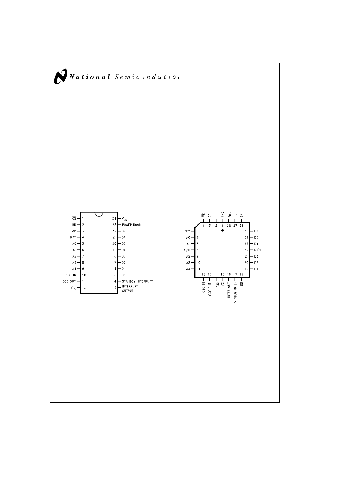
Connection Diagrams
Dual-In-Line Package
TL/F/11070– 1
Top View
Order Number MM58167BN
See NS Package Number N24A
PCC Package
TL/F/11070– 2
Top View
Order Number MM58167BV
See NS Package Number V28A
TRI-STATEÉis a registered trademark of National Semiconductor Corporation.
C
1995 National Semiconductor Corporation RRD-B30M105/Printed in U. S. A.
Page 2
Absolute Maximum Ratings
If Military/Aerospace specified devices are required,
please contact the National Semiconductor Sales
Office/Distributors for availability and specifications.
Voltage at All Pins V
SS
b
0.3V to V
DD
a
0.3V
Operating Temperature 0§Cto70§C
Storage Temperature
b
65§Ctoa150§C
V
DD
b
V
SS
6.0V
Lead Temperature (Soldering, 10 sec.) 300§C
Electrical Characteristics V
SS
e
0V, 0§CsT
A
s
70§C
Parameter Conditions Min Max Units
Supply Voltage
V
DD
Outputs Enabled 4.5 5.5 V
V
DD
POWER DOWN Mode 2.2 5.5 V
Supply Current
I
DD
, Dynamic Outputs TRI-STATE
É
f
IN
e
32.768 kHz, V
DD
e
5.5V
20 mA
V
IH
t
V
DD
b
0.3V
V
IL
s
V
SS
a
0.3V
IDD, Dynamic Outputs TRI-STATE
f
IN
e
32.768 kHz, V
DD
e
5.5V 5 mA
V
IH
e
2.0V, V
IL
e
0.8V
Input Voltage
Logical Low 0.0 0.8 V
Logical high 2.0 V
DD
V
Input Leakage Current V
SS
s
V
IN
s
V
DD
b
11mA
Output Impedance I/O and INTERRUPT OUT
Logical Low V
DD
e
4.5V, I
OL
e
1.6 mA 0.4 V
Logical High V
DD
e
4.5V, I
OH
eb
400 mA 2.4 V
I
OH
eb
10 mA 0.8 V
DD
V
TRI-STATE V
SS
s
V
OUT
s
V
DD
b
11mA
Output Impedance RDY and STANDBY INTERRUPT
(Open Drain Devices)
Logical Low, Sink V
DD
e
4.5V, I
OL
e
1.6 mA 0.4 V
Logical High, Leakage V
OUT
s
V
DD
10 mA
2
Page 3
Functional Description
Real Time Counter
The real time counter is divided into 4-bit digits with 2 digits
being accessed during any read or write cycle. Each digit
represents a BCD number and is defined in Table I. Any
unused bits are held at a logical zero during a read and
ignored during a write. An unused bit is any bit not necessary to provide a full BCD number. For example tens of
hours cannot legally exceed the number 2, thus only 2 bits
are necessary to define the tens of hours. The other 2 bits in
the tens of hours digit are unused. The unused bits are designated in Table I as dashes.
The addressable portion of the counter is from milliseconds
to months. The counter itself is a ripple counter. The ripple
delay is less than 60 ms above 4.5V and 300 ms at 2.2V.
RAM
56 bits of RAM are contained on-chip. These can be used
for any necessary power down storage or as an alarm latch
for comparison to the real time counter. The data in the
RAM can be compared to the real time counter on a digit
basis. The only digits that are not compared are the unit ten
thousandths of seconds and tens of days of the week
(these are unused in the real time counter). If the two most
significant bits of any RAM digit are ones, then this RAM
location will always compare. The rule of thumb for an
‘‘alarm’’ interrupt is: All nibbles of higher order than specified are set to C hex (always compare). All nibbles lower
than specified are set to ‘‘zero’’. As an example, if an alarm
is to occur everyday at 10:15 a.m., configure the bits in RAM
as shown in Table II.
The RAM is formatted the same as the real time counter, 4
bits per digit, 14 digits, however there are no unused bits.
The unused bits in the real time counter will compare only to
zeros in the RAM.
An address map is shown in Table III.
Interrupts and Comparator
There are two interrupt outputs. The first is the INTERRUPT
OUTPUT (a true high signal). This output can be programmed to provide 8 different output signals. They are:
10 Hz, once per second, once per minute, once per hour,
once a day, once a week, once a month, and when a RAM/
real time counter comparison occurs. To enable the output
a one is written into the interrupt control register at the bit
location corresponding to the desired output frequency (
Fig-
ure 1
). Once one or more bits have been set in the interrupt
control register, the corresponding counter’s rollover to its
reset state will clock the interrupt status register and cause
the interrupt output to go high. To reset the interrupt and to
identify which frequency caused the interrupt, the interrupt
status register is read. Reading this register places the contents of the status register on the data bus. The interrupting
frequency will be identified by a one in the respective bit
position. Removing the read will reset the interrupt.
The second interrupt is the STANDBY
INTERRUPT (open
drain output, active low). This interrupt occurs when enabled
and when a RAM/real time counter comparison occurs. The
STANDBY
INTERRUPT is enabled by writing a one on the
D0 line at address 16
H
or disabled by writing a zero on the
D0 line. This interrupt is not triggered by the edge of the
compare signal, but rather by the level. Thus if the compare
is enabled when the STANDBY
INTERRUPT is enabled, the
interrupt will turn on immediately.
TABLE I. Real Time Counter Format
Units
Max
Tens
Max
Counter Addressed
D0 D1 D2 D3
BCD
D4 D5 D6 D7
BCD
Code Code
Milliseconds (00H) Ð Ð Ð Ð 0 D4 D5 D6 D7 9
Hundredths and Tenths Sec (01
H
) D0 D1 D2 D3 9 D4 D5 D6 D7 9
Seconds (02
H
) D0 D1 D2 D3 9 D4 D5 D6 Ð 5
Minutes (03
H
) D0 D1 D2 D3 9 D4 D5 D6 Ð 5
Hours (04H) D0 D1 D2 D3 9 D4 D5 Ð Ð 2
Day of the Week (05
H
)D0D1D2Ð7ÐÐÐÐ0
Day of the Month (06
H
) D0 D1 D2 D3 9 D4 D5 Ð Ð 3
Month (07
H
)D0D1D2D3 9 D4 Ð Ð Ð 1
(Ð) indicates unused bits
3
Page 4

Functional Description (Continued)
TABLE II. Clock RAM Bit Map for Alarm Interrupt Everyday at 10:15 a.m.
Address
Data
Function Hi Nibble Lo Nibble
43210765 4321 0
Milliseconds 0 1 0 0 0 0 0 0 0 No RAM Exists
Hundredths and
010010000000 0
Tenths of Seconds
Seconds 0 1 0 1 0 0 0 0 0 0 0 0 0
Minutes 0 1 0 1 1 0 0 0 1 0 1 0 1
Hours 0 1 1 0 0 0 0 0 1 0 0 0 0
Day of Week 0 1 1 0 1 No RAM Exists 1 1 X X
Day of Month 0 1 1 1 0 1 1 X X 1 1 X X
Months 0 1 1 1 1 1 1 X X 1 1 X X
TABLE III. Address Codes and Function
A4 A3 A2 A1 A0 Function
0 0 0 0 0 CounterÐMilliseconds
0 0 0 0 1 CounterÐHundredths and Tenths of Seconds
0 0 0 1 0 CounterÐSeconds
0 0 0 1 1 CounterÐMinutes
0 0 1 0 0 CounterÐHours
0 0 1 0 1 CounterÐDay of Week
0 0 1 1 0 CounterÐDay of Month
0 0 1 1 1 CounterÐMonth
0 1 0 0 0 RAMÐMilliseconds
0 1 0 0 1 RAMÐHundredths and Tenths of Seconds
0 1 0 1 0 RAMÐSeconds
0 1 0 1 1 RAMÐMinutes
0 1 1 0 0 RAMÐHours
0 1 1 0 1 RAMÐDay of Week
0 1 1 1 0 RAMÐDay of Month
0 1 1 1 1 RAMÐMonths
1 0 0 0 0 Interrupt Status Register
1 0 0 0 1 Interrupt Control Register
1 0 0 1 0 Counters Reset
1 0 0 1 1 RAM Reset
1 0 1 0 0 Status Bit
1 0 1 0 1 GO Comand
1 0 1 1 0 STANDBY
INTERRUPT
1 1 1 1 1 Test Mode
All others unused
The comparator is a cascaded exclusive NOR. Its output is
latched 61 ms after the rising edge of the 1 kHz clock signal
(input to the milliseconds counter). This allows the counter
to ripple through before looking at the comparator. For operation at less than 4.5V, the thousandths of seconds counter
should not be included in a compare because of the possibility of having a ripple delay greater than 61 ms. (For output
timing see Interrupt Timing.)
Power Down Mode
The POWER
DOWN input is essentially a second chip select. It disables all inputs and outputs except for the
STANDBY
INTERRUPT. When this input is at a logical zero,
the device will not respond to any external signals. It will,
however, maintain timekeeping and turn on the STANDBY
INTERRUPT if programmed to do so. (The programming
must be done before the POWER
DOWN input goes to a
4
Page 5

Functional Description (Continued)
logical zero.) When switching V
DD
to the standby or power
down mode, the POWER
DOWN input should go to a logical
zero at least 1 ms before V
DD
is switched. When switching
V
DD
all other inputs must remain between V
SS
b
0.3V and
V
DD
a
0.3V. When restoring VDDto the normal operating
mode, it is necessary to insure that all other inputs are at
valid levels before switching the POWER
DOWN input back
to a logical one. These precautions are necessary to insure
that no data is lost or altered when changing to or from the
power down mode.
Counter and RAM Resets; GO Command
The counters and RAM can be reset by writing all 1’s (FF) at
address 12
H
or 13Hrespectively.
A write pulse at address 15Hwill reset the thousandths,
hundredths, tenths, units, and tens of seconds counters.
This GO command is used for precise starting of the clock.
The data on the data bus is ignored during the write. If the
seconds counter is at a value greater than 39 when the GO
is issued, the minute counter will increment; otherwise the
minute counter is unaffected. This command is not necessary to start the clock, but merely a convenient way to start
precisely at a given minute.
Status Bit
The status bit is provided to inform the user that the clock is
in the process of rolling over when a counter is read. The
status bit is set if this 1 kHz clock occurs during or after any
counter read. This tells the user that the clock is rippling
through the real time counter. Because the clock is rippling,
invalid data may be read from the counter. If the status bit is
set following a counter read, the counter should be reread.
The status bit appears on D0 when address 14
H
is read. All
the other data lines will zero. The bit is set when a logical
one appears. This bit should be read every time a counter
read or after a series of counter reads are done. The trailing
edge of the read at address 14
H
will reset the status bit.
Using the Rollover Status Bit
If a single read of any clock counter is made, it should be
followed by reading the rollover status bit.
Example: Read months, then read rollover status.
If a sequential read of the clock counters is made, then the
rollover status bit should be read after the last counter is
read.
Example: Read hours, minutes, seconds, then read the rollover status.
Oscillator
The oscillator used is the standard Pierce parallel resonant
oscillator. Externally, 2 capacitors, a 20 MX resistor and the
crystal are required. The 20 MX resistor is connected between OSC IN and OSC OUT to bias the internal inverter in
the linear region. For micropower crystals a resistor in series
with the oscillator output may be necessary to insure the
crystal is not overdriven. This resistor should be approximately 200 kX. The capacitor values should be typically
20 pF – 25 pF. The crystal frequency is 32,768 Hz.
The oscillator input can be externally driven, if desired. In
this case the oscillator output should be left floating and the
oscillator input levels should be within 0.3V of the supplies.
A ground line or ground plane between pins 9 and 10 may
be necessary to reduce interference of the oscillator by the
A4 address.
Control Lines
The READ
, WRITE, AND CHIP SELECT signals are active
low inputs. The READY
signal is an open drain output. At
the start of each read or write cycle the READY
line (open
drain) will pull low and will remain low until valid data from a
chip read appears on the bus or data on the bus is latched
in during a write. READ
and WRITE must be accompanied
by a CHIP SELECT
(see
Figures 3
and4for read and write
cycle timing).
During a read or write, address bits must not change while
chip select and control strobes are low.
Test Mode
The test mode is for production testing. It allows the counters to count at a higher than normal rate. In this mode the
32.768 kHz oscillator input is connected directly to the ten
thousandths of seconds counter. The chip select and write
lines must be low and the address must be held at 1F
H
.
TL/F/11070– 3
FIGURE 1. Interrupt Register Format
5
Page 6

Functional Description (Continued)
Typical Supply Current
vs Supply VoltageStandby Interrupt
during Power DownTypical Characteristics
TL/F/11070– 4 TL/F/11070– 5
FIGURE 2
Interrupt Timing 0
§
CsT
A
s
70§C, 4.5VsV
DD
s
5.5V, V
SS
e
0V
Symbol Parameter Min Max Units
t
INTON
Status Register Clock to INTERRUPT OUTPUT
5 ms
(Pin 13) High (Note 1)
t
SBYON
Compare Valid to STANDBY INTERRUPT
5 ms
(Pin 14) Low (Note 1)
t
INTOFF
Trailing Edge of Status Register
5 ms
Read to INTERRUPT OUTPUT Low
t
SBYOFF
Trailing Edge of Write Cycle
(D0
e
0; Addresse16H) to STANDBY 5 ms
INTERRUPT
Off (High Impedance State)
Note 1: The status register clocks are: the corresponding counter’s rollover to its reset state or the compare becoming valid. The compare becomes valid 61 ms
after the 1/10,000 of a second counter is clocked, if the real time counter data matches the RAM data.
Read Cycle Timing 0
§
CsT
A
s
70§C, 4.5VsV
DD
s
5.5V, V
SS
e
0V
Symbol Parameter Min Max Units
t
AR
Address Bus Valid to Read Strobe (Note 3) 100 ns
t
CSR
Chip Select to Read Strobe (Note 2) 0 ns
t
RRY
Read Strobe to Ready Strobe 150 ns
t
RYD
Ready Strobe to Data Valid 800 ns
t
AD
Address Bus Valid to Data Valid 1050 ns
t
RH
Data Hold Time from Trailing Edge of Read Strobe 0 ns
t
HZ
Trailing Edge of Read Strobe to TRI-STATE Mode 250 ns
t
RYH
Read Hold Time after Ready Strobe 0 ns
t
RA
Address Bus Hold Time from Trailing Edge of Read Strobe 50 ns
t
RYDV
Rising Edge of Ready to Data Valid 100 ns
Note 2: When reading, a deselect time of 500 ns minimum must occur between counter reads. Deselect is: CSe1or(WR)#(RD)e1.
Note 3: If t
AR
e
0 and Chip Select, Address Valid or Read are coincident then they must exist for 1050 ns.
6
Page 7

Write Cycle Timing 0
§
CsT
A
s
70§C, 4.5VsV
DD
s
5.5V, V
SS
e
0V
Symbol Parameter Min Max Units
t
AW
Address Valid to Write Strobe 100 ns
t
CSW
Chip Select to Write Strobe 0 ns
t
DW
Data Valid before Write Strobe 100 ns
t
WRY
Write Strobe to Ready Strobe 150 ns
t
RY
Ready Strobe Width 800 ns
t
RYH
Write Hold Time after Ready Strobe 0 ns
t
WD
Data Hold Time after Write Strobe 110 ns
t
WA
Address Hold Time after Write Strobe 50 ns
Note 4: If data changes while CS and WR are low, then they must remain coincident for 1050 ns after the data change to ensure a valid write. Data bus loading is
100 pF. Ready output loading is 50 pF and 3 kX pull-up.
Input and output AC timing levels:
Logical one
e
2.0V
Logical zero
e
0.8V
Read and Write Cycle Timing Diagrams
TL/F/11070– 6
FIGURE 3. Read Cycle Timing
TL/F/11070– 7
FIGURE 4. Write Cycle Timing
7
Page 8

Typical Applications
R1e20 MXg20%
C1
e
6pFb36 pF
R2 to be selected
based on crystal used.
TL/F/11070– 8
Note 5: A ground line or ground plane guard trace should be included between pins 9 and 10 to insure the oscillator is not disturbed by the address line.
FIGURE 5. Typical Connection Diagram
TL/F/11070– 9
Note 6: Must use 8238 or equivalent logic to insure advanced I/OW pulse; so that the ready output of the MM58167B is valid by the end of w2 during the T2
microcycle.
Note 7: t
w2
t
t
RS8080
a
t
DL8238
a
t
WRY58167B
.
FIGURE 6. 8080 System Interface with Battery Backup
8
Page 9

Block Diagram
TL/F/11070– 10
FIGURE 7
Physical Dimensions inches (millimeters)
Molded Dual-In-Line Package (N)
Order Number MM58167BN
NS Package Number N24A
9
Page 10

MM58167B Microprocessor Real Time Clock
Physical Dimensions inches (millimeters) (Continued)
PCC Package (V)
Order Number MM58167BV
NS Package Number V28A
LIFE SUPPORT POLICY
NATIONAL’S PRODUCTS ARE NOT AUTHORIZED FOR USE AS CRITICAL COMPONENTS IN LIFE SUPPORT
DEVICES OR SYSTEMS WITHOUT THE EXPRESS WRITTEN APPROVAL OF THE PRESIDENT OF NATIONAL
SEMICONDUCTOR CORPORATION. As used herein:
1. Life support devices or systems are devices or 2. A critical component is any component of a life
systems which, (a) are intended for surgical implant support device or system whose failure to perform can
into the body, or (b) support or sustain life, and whose be reasonably expected to cause the failure of the life
failure to perform, when properly used in accordance support device or system, or to affect its safety or
with instructions for use provided in the labeling, can effectiveness.
be reasonably expected to result in a significant injury
to the user.
National Semiconductor National Semiconductor National Semiconductor National Semiconductor
Corporation Europe Hong Kong Ltd. Japan Ltd.
1111 West Bardin Road Fax: (
a
49) 0-180-530 85 86 13th Floor, Straight Block, Tel: 81-043-299-2309
Arlington, TX 76017 Email: cnjwge@tevm2.nsc.com Ocean Centre, 5 Canton Rd. Fax: 81-043-299-2408
Tel: 1(800) 272-9959 Deutsch Tel: (
a
49) 0-180-530 85 85 Tsimshatsui, Kowloon
Fax: 1(800) 737-7018 English Tel: (
a
49) 0-180-532 78 32 Hong Kong
Fran3ais Tel: (
a
49) 0-180-532 93 58 Tel: (852) 2737-1600
Italiano Tel: (
a
49) 0-180-534 16 80 Fax: (852) 2736-9960
National does not assume any responsibility for use of any circuitry described, no circuit patent licenses are implied and National reserves the right at any time without notice to change said circuitry and specifications.
 Loading...