

Page 1
MITSUMI
Low-Ripple, Low-Saturation CMOS Regulators MM309X/MM310X Series
Low-Ripple, Low-Saturation CMOS Regulators
Monolithic IC MM309X, MM310X Series
Outline
This is a voltage regulator IC developed using the CMOS process.
Use of the CMOS process allows low current consumption, and it has superior ripple rejection ratio and
transient response compared to conventional CMOS process regulator ICs, making it ideal for use in portable
communications devices.
Ceramic capacitors can be used for the output capacitors.
Ideal for small, portable devices as SOT-25 and WLCSP are used for the package.
Features
1. Super low consumption current
45µA typ. (when not loaded, excluding the CE terminal current)
2. Super low consumption current (when off) 0.1µA typ.
3. High precision output voltage ±2%
4. Output current 150mA
5. Input/output voltage difference 0.23V typ. (Io=100mA, 3V output)
6. High ripple rejection ratio 80dB typ.
7. Built-in short-circuit restriction circuit 30mA typ.
8. Wide operating temperature range
-
30~+85°C
9. Output voltage 1.8~5.0V (0.1V step)
Applications
1. Constant voltage power supply for devices that use batteries
2. Constant voltage power supply for portable communications devices
3. Constant voltage power supply for household electronics products
Package
SOT-25, WLCSP-4 (MM309X),
WLCSP-5 (MM310X)
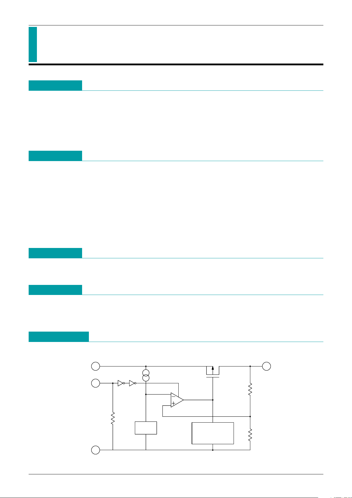
Block Diagram
V
GND
1
VDD
3
Current
Limit
REF
OUTV
2
CE
4
Page 2
MITSUMI
Low-Ripple, Low-Saturation CMOS Regulators MM309X/MM310X Series
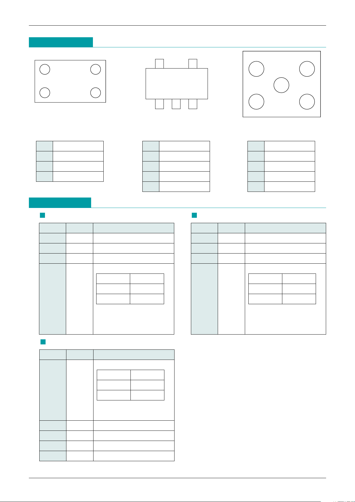
Pin Assignment
Pin Description
Pin No. Pin name
Functions
1 GND GND pin
2 V
OUT
Regulator output pin
3 VDD Voltage-supply pin
ON/OFF-Control pin
4 CE
Connect CE pin with V
DD
pin, when it is not used.
CE OUTPUT
L OFF
HON
4
1
3
2
WLCSP-4
(BOTTOM VIEW)
1 GND
2 V
OUT
3 VDD
4 CE
54
123
SOT-25A
(TOP VIEW)
1 VOUT
2 GND
3 V
DD
4 CE
5 V
DD
4
2
3
5
1
WLCSP-5
(BOTTOM VIEW)
1 CE
2 GND
3 V
OUT
4 VDD
5 NC
WLCSP-4
Pin No. Pin name
Functions
1 V
OUT
Regulator output pin
2 GND GND pin
3,5 V
DD Voltage-supply pin
ON/OFF-Control pin
4 CE
Connect CE pin with V
DD
pin, when it is not used.
CE OUTPUT
L OFF
HON
SOT-25A
Pin No. Pin name
Functions
ON/OFF-Control pin
1 CE
Connect CE pin with V
DD
pin, when it is not used.
2 GND GND pin
3 V
OUT
Regulator output pin
4 V
DD Voltage-supply pin
5 NC
CE OUTPUT
L OFF
HON
WLCSP-5
Page 3
MITSUMI
Low-Ripple, Low-Saturation CMOS Regulators MM309X/MM310X Series
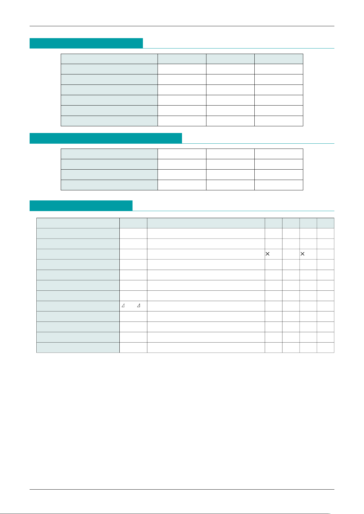
Electrical Characteristics
(VDD=VOUT typ.+1V, VCE=VDD, Ta=25°C
unless otherwise speciffied
)
Item Symbol Measurement conditions Min. Typ. Max. Unit
Input Current(OFF) I
DDOff VCE=0V 0.1 1.0 µA
No-Load Input Current I
DD 45 100 µA
Output Voltage V
OUT 1mA
<
=
I
OUT
<
=
30mA 0.98 1.02 V
Line Regulation V
LINE VDD=VO typ.+0.5~6V IOUT=30mA 0.05 0.20
%/V
Load Regulation VLOAD 1mA
<
=
I
OUT
<
=
80mA 20 45 mV
Dropout Voltage Vio Please refer to another page V
Ripple Rejection
*
1 RR Please refer to another page dB
V
OUT
Temperature Coefficient *1
V
OUT
/ T
IOUT=10mA -40mA
<
=
T
OPT
<
=
85°C ±100
ppm/°C
Output Short-Circuit Current *1 Ilim VO=0V 30 mA
CE Pull-down Resistance R
pd 2.5 5 15 MΩ
CE High Threshold voltage V
CEH 1.5 VDD V
CE Low Threshold voltage V
CEL 0 0.25 V
Absolute Maximum Ratings
(Ambient Temperature, Ta=25°C)
Item Symbol Ratings Unit
Storage Temperature T
STG
-
55~+125 °C
Supply Voltage V
DD 7V
CE Input Voltage V
OUT
-
0.3~VDD+0.3 V
Output Voltage V
OUT
-
0.3~VDD+0.3 V
Output Current I
Omax. 200 mA
Power Dissipation Pd 190 mW
Recommended Operating Conditions
(Ambient Temperature, Ta=25°C)
Item Symbol Ratings Unit
Operating Temperature T
jop
-
40~85 °C
Operating Voltage V
OP 2~6 V
Output Current I
O 0~150 mA
Note: *1 design guaranteed.
Page 4

MITSUMI
Low-Ripple, Low-Saturation CMOS Regulators MM309X/MM310X Series
Electrical Characteristics 2
(VDD=VOUT
typ.+1V,
V
CE=VDD Ta=25°C unless otherwise speciffied)
PARAMETER
Product Output Voltage Dropout Voltage Ripple Regulation
*
1
Name V
OUT (V) Vio (V) RR (db)
TEST CONDISIONS
MIN. TYP. MAX.
TEST CONDISIONS
TYP. MAX.
TEST CONDISIONS
TYP. MAX.
MM3091J 1.764 1.800 1.836
MM3091K 1.862 1.900 1.938
MM3092A 1.960 2.000 2.040
MM3092B 2.058 2.100 2.142
0.25 0.35
MM3092C 2.156 2.200 2.244
MM3092D 2.254 2.300 2.346
MM3092E 2.352 2.400 2.448
MM3092F 2.450 2.500 2.550
0.24 0.29
MM3092G 2.548 2.600 2.652
MM3092H 2.646 2.700 2.754
MM3092J 2.744 2.800 2.856
MM3092K 2.842 2.900 2.958 80
MM3093A 2.940 3.000 3.060
MM3093B 3.038 3.100 3.162
MM3093C 3.136 3.200 3.264
MM3093D 3.234 3.300 3.366
MM3093E 3.332 3.400 3.468
MM3093F 3.430 3.500 3.570
MM3093G 3.528 3.600 3.672
MM3093H 3.626 3.700 3.774
MM3093J 3.724 3.800 3.876
MM3093K 3.822 3.900 3.978 0.23 0.26
MM3094A 3.920 4.000 4.080
MM3094B 4.018 4.100 4.182
MM3094C 4.116 4.200 4.284
MM3094D 4.214 4.300 4.386
MM3094E 4.312 4.400 4.488
MM3094F 4.410 4.500 4.590
70
MM3094G 4.508 4.600 4.692
MM3094H 4.606 4.700 4.794
MM3094J 4.704 4.800 4.896
MM3094K 4.802 4.900 4.998
MM3095A 4.900 5.000 5.100
1mA
<
=
I
OUT
<
=
30mA
I
OUT
=100mA
2.0
<
=
V
OUT
<
=
2.3
f=1kHz
Vripple=
0.5V
1.8
<
=
V
OUT
<
=
4.0
4.1
<
=
V
OUT
<
=
5.0
2.4
<
=
V
OUT
<
=
2.7
2.8
<
=
V
OUT
<
=
5.0
*
2
Note:
*
1 design guaranteed.
Note:
*
2 The parameter is not guaranteed in the model less than VOUT=2V.
Page 5

MITSUMI
Low-Ripple, Low-Saturation CMOS Regulators MM309X/MM310X Series
Measuring Circuit
VDD
VOUT
3
2
CE
GND
4A
1
A
V
A
Ceramic
*
Ceramic
2.2µF
2.2µF
Application Circuits
VDD
VOUT
3
2
CE
GND
4
1
Ceramic
*
To load
Ceramic
2.2µF
2.2µF
(reference example of external parts)
· Output Capacitor Ceramic Capacitor 2.2µF (Output voltage : 2.5~5.0V)
Ceramic Capacitor 4.7µF (Output voltage : 1.8~2.5V)
· Input Capacitor Ceramic Capacitor 2.2µF
Note
1. The output capacitor is required between output and GND to prevent oscillation.
2. The ESR of capacitor must be defined in ESR stability area.
It is possible to use a ceramic capacitor without ESR resistance for output.
The ceramic capacitor must be used more than 2.2µF or 4.7µF and B temperature characteristics.
3. The wire of VCC and GND is required to print full ground plane for noise and stability.
The input capacitor must be connected a distance of less than 1cm from input pin.
*
Temperature Characteristics: B
Page 6

MITSUMI
Low-Ripple, Low-Saturation CMOS Regulators MM309X/MM310X Series
Output Voltage No-Load Input Current
0.0
3165420
Input Voltage VIN(V)
1.5
1.0
0.5
2.0
3.0
2.5
Output Voltage VO(V)
IO=150mA
IO=30mA
IO=1mA
0
3165420
Input Voltage VIN(V)
30
25
20
15
10
5
40
35
50
45
No-Load Input Current IDD(µA)
Line Regulation
-1.0
5.543.5 64.5 53
Input Voltage VIN(V)
0.0
-0.2
-0.4
-0.6
-0.8
1.0
0.6
0.4
0.2
0.8
Line Regulation Vline(mV)
IO=30mA
Load Regulation
Dropout Voltage
-150
50 1501000
Output Current IO(mA)
0
-50
-100
150
100
50
Load Regulation Vload(mV)
0.00
50 1501000
Output Current IO(mA)
0.20
0.10
0.40
0.30
Dropout Voltage Vio(V)
VIN=2.6V, IO=10mA
Current Limit
0.0
100 200 4003000
Output Current IO(mA)
1.5
0.5
1.0
3.0
2.0
2.5
Output Voltage Vio(V)
VIN=3.8V
V
IN=5.0V
V
IN=6.0V
Characteristics
(2.8V product Except where noted therwise, Ta=25°C, VIN=VO+1V, VCE=VDD, CIN=2.2µF, CO=2.2µF)
Page 7

MITSUMI
Low-Ripple, Low-Saturation CMOS Regulators MM309X/MM310X Series
GND Pin Current ESR
0
25 50 75 100 1501250
Output Current (mA)
50
40
20
10
30
100
60
70
80
90
GND pin Current(µA)
Output Current IO (mA)
ESR(Ω)
1000
100
1
0.1
10
0.01
0 30 60 90 120 150
Stable area
Instable area
Characteristics
(2.8V product Except where noted therwise, Ta=25°C, VIN=VO+1V, VCE=VDD, CIN=2.2µF, CO=2.2µF)
Output Voltage-Ambient Temperature Ripple Rejection
2.72
-25 0 25 50 75 125
I
O=10mA
100-50
Temperature T(˚C)
2.78
2.74
2.76
2.84
2.80
2.82
Output voltage Vo(V)
Frequency(kHz)
Ripple rejection(dB)
-90
-80
-70
-60
-50
-40
-30
-20
-10
0
0.01 0.1 1 10 100 1000
IO=100mA
IO=150mA
IO=30mA
IO=1mA
Page 8

MITSUMI
Low-Ripple, Low-Saturation CMOS Regulators MM309X/MM310X Series
Rise Time (VCE=0 2.0V)
Input Transient Response (VDD=3.8V 4.8V)
VCE VCE=0V
V
O
VCE=2V
V
O=0V
V
O=2.8V
10µ
S
VO:1V/div
VCE:1V/div
CH1=1V
DC=10:1
CH2=1V 10µS=div
NORM:10MS/
S
DC=10:1
VO
VDD
VDD=3.8V
V
DD=4.8V
200µ
S
VDD:2V/div
VO:10mV/div
CH1=10mV
AC=10:1
CH2=2V 200µS/div
NORM:5MS/
S
DC=10:1
Characteristics
(2.8V product Except where noted therwise, Ta=25°C, VIN=VO+1V, VCE=VDD, CIN=2.2µF, CO=2.2µF)
Load Transient Response (V
O
=1mA 100mA, CO=2.2µF) Load Transient Response (V
O
=1mA 100mA, CO=1.0µF)
VO
IO
IO=1mA
I
O=100mA
500µ
S
CH1=10mV
DC=1:1
CH3=20mV
AC=10:1
IO:50mA/div
VO:10mV/div
VO
IO
IO=1mA
I
O=100mA
500µ
S
CH1=10mV
DC=1:1
CH3=20mV
AC=10:1
IO:50mA/div
VO:10mV/div
 Loading...