

Page 1

MITSUMI
CMOS Regulator MM303X Series
CMOS Regulator
Monolithic IC MM303X Series
Outline
This IC is a voltage regulator IC developed using the CMOS process. Super low consumption current of
1.5 µA typ. (MM303X) (when not loaded) has been achieved through the use of the CMOS process. Also, the
output voltage has a high accuracy of ±2%.
Features
1. Super low consumption current
1.5µA typ. (when not loaded, excluding the CE terminal current)
2. Super low consumption current (when off) 0.1µA typ.
3. High precision output voltage ±2%
4. Input/output voltage difference 40mV typ. (Io=1mA MM3033A)
5. Good input stability 0.05%/V typ.
6. Built-in short-circuit restriction circuit 60mA typ.
7. Wide operating temperature range
-
30~+85°C
8. Output voltage 1.7~5.5V (0.1V step)
Applications
1. Devices that use batteries
2. Portable communications devices
3. Household electronics products
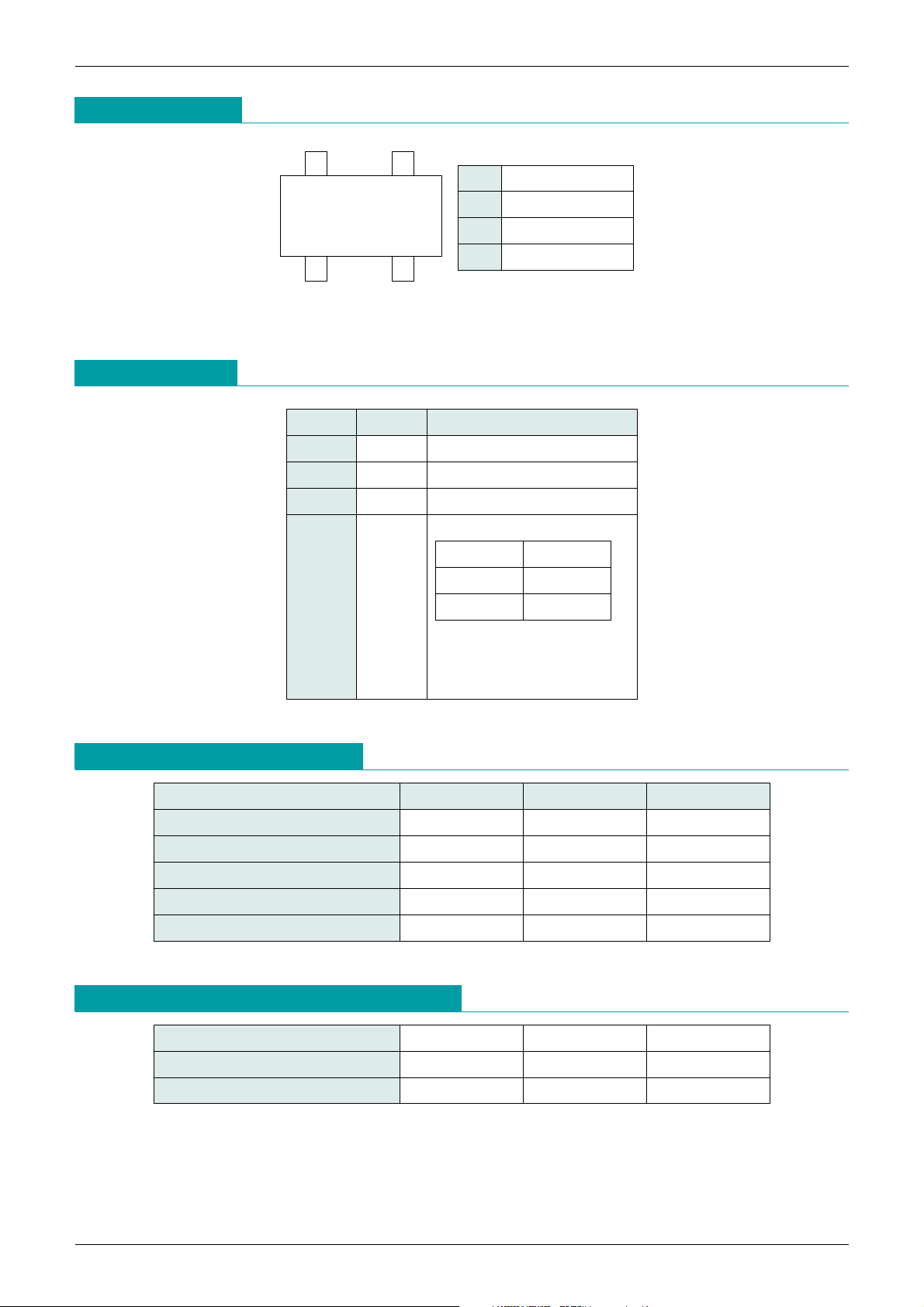
Package
SC-82AB
Block Diagram
Page 2
MITSUMI
CMOS Regulator MM303X Series
Pin Assignment
12
43
SC-82AB
(TOP VIEW)
1 GND
2 V
DD
3 VOUT
4 CE
Pin Description
Pin No. Pin name
Functions
1 GND GND Pin
2 V
DD Voltage-Supply pin
3 V
OUT Regulator output pin
No connection pin
4 CE
ON/OFF-Control pin
Connect CE-pin with VDD-
pin,when it is not used.
CE OUTPUT
L OFF
HON
Absolute Maximum Ratings
(Ambient Temperature, Ta=25°C)
Item Symbol Ratings Unit
Storage Temperature T
STG
-
40~+125 °C
Operating Temperature T
OPR
-
30~+85 °C
Supply Voltage V
DD
-
0.3~+9 V
Output Current I
OUT 150 mA
Allowable loss Pd 150 (Alone) mW
Recommended Operating Conditions
(Ambient Temperature, Ta=25°C)
Item Symbol Ratings Unit
Operating Temperature T
OP
-
30~+85 °C
Supply Voltage V
OP VOUT+0.3~8 V
Page 3
MITSUMI
CMOS Regulator MM303X Series
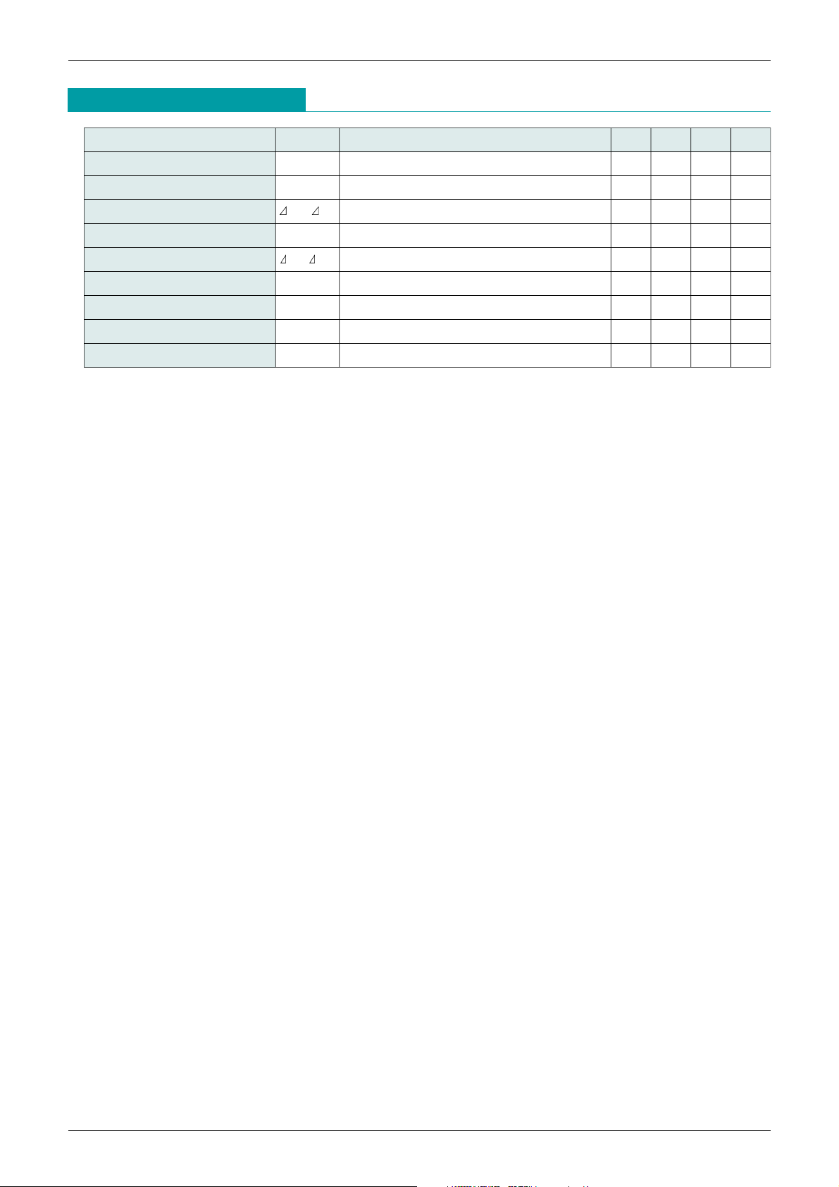
Electrical Characteristics
(Ambient Temperature, Ta=25°C, VIN=VCE)
Item Symbol Measurement conditions Min. Typ. Max. Unit
Quiescent Current I
SS VIN=VOUT+2.0V 1.5 3.0 µA
Input Current(OFF) Istandby V
IN=VOUT+2.0V, VCE=0V 0.1 1.0 µA
Line Regulation
V
OUT
/ V
IN
IOUT=1mA, VOUT+0.5V
<
=
V
IN
<
=
8V 0 0.05 0.20
%/V
Input Voltage VIN 8V
Output voltage temperature coefficient
V
OUT
/ Vopt
IOUT=10mA-30°C
<
=
T
OPT
<
=
85°C ±100
ppm/°C
Short current Ilim VIN=VOUT+2.0V, VOUT=0V 60 mA
CE pin current when ON I
CE VIN=VOUT+2.0V 0.1 1.0 µA
CE input voltage "H" V
CEH VIN=VOUT+2.0V VIN
-
1VIN V
CE input voltage "L" V
CEL VIN=VOUT+2.0V 0.25 V
Page 4

MITSUMI
CMOS Regulator MM303X Series
Electrical Characteristics 2
(Ambient Temperature, Ta=25°C, VIN=VCE)
PARAMETER
Product Output Voltage Output Current Load Regulation
Input-Output differential Voltage
Name VOUT (V) IOUT (mA) VOUT/ IOUT (mV) VDIF (V)
TEST CONDISIONS
MIN. TYP. MAX.
TEST CONDISIONS
MIN. TYP.
TEST CONDISIONS
TYP. MAX.
TEST CONDISIONS
TYP. MAX.
MM3031H 1.666 1.700 1.734
MM3031J 1.764 1.800 1.836
MM3031K 1.862 1.900 1.938
MM3032A 1.960 2.000 2.040
MM3032B 2.058 2.100 2.142
MM3032C 2.156 2.200 2.244
MM3032D 2.254 2.300 2.346
MM3032E 2.352 2.400 2.448
MM3032F 2.450 2.500 2.550
MM3032G 2.548 2.600 2.652
MM3032H 2.646 2.700 2.754
MM3032J 2.744 2.800 2.856
MM3032K 2.842 2.900 2.958
MM3033A 2.940 3.000 3.060
MM3033B 3.038 3.100 3.162
MM3033C 3.136 3.200 3.264
MM3033D 3.234 3.300 3.366
MM3033E 3.332 3.400 3.468
MM3033F 3.430 3.500 3.570
MM3033G 3.528 3.600 3.672
MM3033H 3.626 3.700 3.774
MM3033J 3.724 3.800 3.876
MM3033K 3.822 3.900 3.978
MM3034A 3.920 4.000 4.080
MM3034B 4.018 4.100 4.182
MM3034C 4.116 4.200 4.284
MM3034D 4.214 4.300 4.386
MM3034E 4.312 4.400 4.488
MM3034F 4.410 4.500 4.590
MM3034G 4.508 4.600 4.692
MM3034H 4.606 4.700 4.794
MM3034J 4.704 4.800 4.896
MM3034K 4.802 4.900 4.998
MM3035A 4.900 5.000 5.100
MM3035B 4.998 5.100 5.202
MM3035C 5.096 5.200 5.304
MM3035D 5.194 5.300 5.406
MM3035E 5.292 5.400 5.508
MM3035F 5.390 5.500 5.610
VIN-
V
OUT
=
2.0V
10µA
<
=
I
OUT
<
=
10mA
V
IN
-
V
OUT
=2.0V
VIN-
V
OUT
=
2.0V
1mA
<
=
I
OUT
<
=
35mA
3035
50
65
80
VIN-
V
OUT
=2.0V
1mA
<
=
I
OUT
<
=
50mA
40
I
OUT=
1mA
60
50
40
35
30
25
90
75
60
55
45
40
VIN-
V
OUT
=2.0V
1mA
<
=
I
OUT
<
=
65mA
50
VIN-
V
OUT
=2.0V
1mA
<
=
I
OUT
<
=
80mA
60
45
60
70
90
Page 5

MITSUMI
CMOS Regulator MM303X Series
Measuring Circuit
Typical Application Circuit
Note: This regulator is not internally compensated and thus requires an external output-capacitor(COUT) for stability.
Page 6

MITSUMI
CMOS Regulator MM303X Series
Characteristics
(3.0V product Ambient Temperature, Ta=25°C)
Input-output Differential Voltage Line Regulation
0.0
503010 40200
Output Current (mA)
0.4
1.6
1.2
0.8
0.2
1.4
1.0
0.6
1.8
2.0
Input-output Differential
Voltage (V)
0.0
62840
Input Voltage (V)
2.0
1.5
1.0
0.5
2.5
3.5
3.0
Output Voltage (V)
Load Regulation
0.0
50 1501000
Output Current (mA)
2.0
1.5
1.0
0.5
2.5
3.5
V
IN=5V
3.0
Output Voltage (V)
Input Current
CE Terminal Input Current VS CE Terminal Input Voltage
0.0
84620
Input Voltage (V)
2.0
1.5
1.0
0.5
2.5
3.0
Input Current (µA)
0.0
62840
CE Terminal Input Voltage (V)
0.4
0.3
0.2
0.1
0.5
CE Terminal Input
Current (µA)
Ripple Rejection
0
1001100.1
Frequency (kHz)
50
40
30
20
10
60
80
70
V
IN=5V DC, 0.5VP-PAC
I
OUT=10mA
Ripple Rejection (dB)
Page 7

MITSUMI
CMOS Regulator MM303X Series
Output Voltage VS Temperature Input Current VS Temperature
Temperature (°C)
2.90
8570
-
54520
-
30
3.06
3.04
3.02
3.00
2.98
2.94
2.92
3.10
2.96
3.08
I
OUT=10mA
Output Voltage (V)
Temperature (°C)
0.0
20
20
-
5
-
30
2.0
0.5
1.0
1.5
2.5
3.0
Input Current (µA)
Power Dissipation
Temperature (°C)
0
12550 10025 750
100
300
200
250
50
150
Alone
Power Dissipation(mW)
On Board (Glass Epoxy Resin)
100 100 1.6mm
0.001
0.01
0.1
1
10
100
0.01
Ceramic capacitor reference data when 1µF.
0.1 1
Stable Region
10 100
1000
IO Output Currente (mA)
ESR (Ω)
ESR Stable region
 Loading...