

Page 1
MITSUMI
13
5
2
4
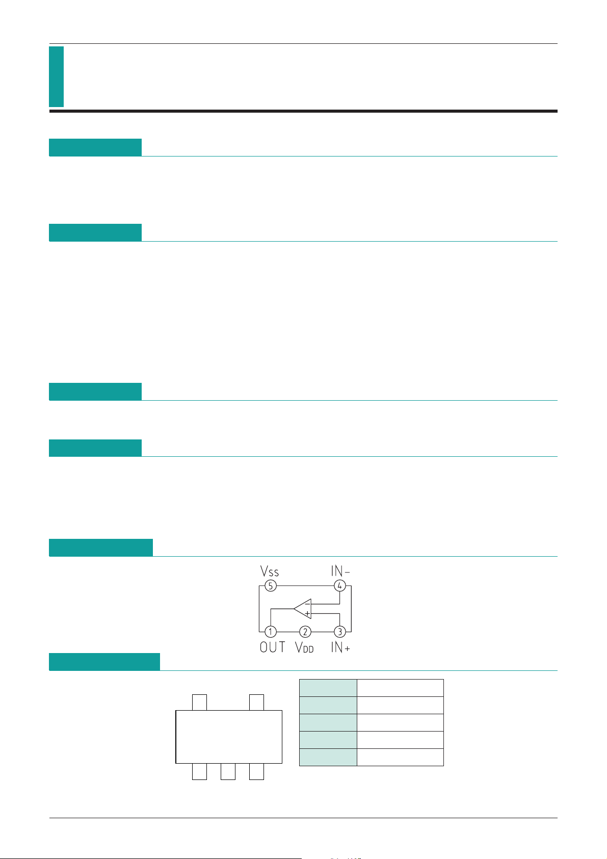
SOT-25
TOP VIEW
CMOS Operational Amplifier (Single) MM3002
CMOS Operational Amplifier (Single)
Monolithic IC MM3002
Outline
This IC is a CMOS (Single) operating amp for which input/output voltage both can be used up to the power
supply voltage. Further, low offset voltage, low drift and low consumption current have been achieved. The
package is the ultra-small SOT-25.
Features
(1) Input voltage range (VDD=3V)
(2) Output voltage range (V
(3) Input offset voltage 1mV typ.
(4) Input offset voltage temperature drift 5µV/°C typ.
(5) Input bias current 5pA typ.
(6) Consumption current 120µA typ.
(7) Output current ±5mA typ.
(8) Through rate 0.6V/µS
DD=3V) 0.03V~2.97V typ.
-
0.1V~VDD+0.1V typ.
Package
SOT-25
Applications
(1) Communication equipment (mobile telephones, cordless telephones, etc.)
(2)
Computers and computer peripherals (notebook PCs, mini PCs, PDA, digital cameras, printers, scanners, etc.)
(3) AV equipment (movies, CD players, MD players, etc.)
(4) Other (navigation equipment, measurement equipment, handy terminals, etc.)
Block Diagram
Pin Assignment
1 OUT
2 V
3 IN+
4IN
5 VSS
DD
-
Page 2

MITSUMI
CMOS Operational Amplifier (Single) MM3002
Pin Description
Pin No. Pin name Functions Internal Equivaalent Circuit
1 OUT Output pin
2 VDD Power supply input pin
3 IN+ Non -inverting input pin
4 IN
-
Inverting input pin
5 VSS VSS PIN
Absolute Maximum Ratings
Item Symbol Ratings Units
Storage temperature T
Operating temperature T
Power supply voltage V
(Except where noted otherwise, Ta=25°C)
STG
OPR
DD max. 10 V
-
40~+125 °C
-
30~+85 °C
Input voltage V
I
-
0.3~VDD+0.3 V
Page 3

MITSUMI
Recommended Operating Conditions
Item Symbol Ratings Units
Operating temperature T
OPR
CMOS Operational Amplifier (Single) MM3002
-
30~+85 °C
Power supply voltage V
Input voltage V
Electrical Characteristics
Item Symbol Measurement conditions
Input offset voltage VOS Rs
Input offset voltage V
temperature Drift Ta
Input bias current IB 25pA
Common - mode
signal rejection ratio
Power supply voltage
rejection ratio
Current consumption I
Input voltage L V
Input voltage H V
Voltage gain A
Gain band area GBW A
Output voltage L V
Output voltage H V
Output flow current I
Output inflow current I
Through rate SR 11 0.6 V/µS
OPR +2.7~+9 V
I 0~VDD V
(Except where noted otherwise, Ta=25°C, VDD=3V, VIN=1.5V)
OS/
Measurement
curcuit
<
10kΩ 113mV
=
Ta=30°C~+85°C 1 5
Min. Typ. Max. Units
µV/
CMRR 1 60 70 dB
PSRR V
DD 3 50 120 240 µA
IL 4
IH 5VDDVDD
V RL
OL 7 0.03 0.05 V
OH 8 2.95 2.97 V
SO 9 2.5 5 mA
SI 10 2.5 5 mA
DD=3V~5V 1 70 90 dB
-
0.1 0 V
+0.1
>
100kΩ 68095 dB
=
V=0dB 6 800 kHz
V
°C
NOTE1 Put capacitors of number µF between VDD-VSS when using.
Measuring Circuit
(Except where noted otherwise, Ta=25°C, VDD=3V, VIN=VDD/2, SW1;A)
Measuring circuit 1
Vo1-VIN
VOS=
CMRR=20log
PSRR=20log
100
100 vi1
vo1 SW1 ; B vi1=1V
(5-3) 100
-
VIN1) - (vo2-VIN2) VIN2, VO2 ; VDD=5V
(vo1
(P-P)
Page 4

MITSUMI
CMOS Operational Amplifier (Single) MM3002
Measuring circuit 2 Measuring circuit 3
IB1+IB2
B=
I
2
Measuring circuit 4 Measuring circuit 5
Measuring circuit 6
Av=20log
vo6 10
vi6 vo6=1V
Measuring circuit 7 Measuring circuit 8
Measuring circuit 9 Measuring circuit 10
4
P-P
Measuring circuit 11
Page 5

MITSUMI
0
0
50
100
150
200
250
300
24681012
Power Supply Voltage (V)
Current Consumption (µA)
(Ta=25°C, VIN=VDD/2)
246810
-
3
-
2
-
1
0
1
2
3
12
Power Supply Voltage (V)
Input Offset Voltage (mV)
(Ta=25°C, VIN=VDD/2)
246810
-
3
-
2
-
1
0
1
2
3
12
Power Supply Voltage (V)
Input Offset Voltage (mV)
(Ta=25°C, VIN=0.5V)
246810
-
3
-
2
-
1
0
1
2
3
12
Power Supply Voltage (V)
Input Offset Voltage (mV)
(Ta=25°C, VIN=VDD
-
0.5V)
-40-
200 20406080
0
50
100
150
200
250
300
100
Ambient Temperature (°C)
Current Consumption (µA)
(VDD=3V, VIN=1.5V)
-40-
200 20406080
-
3
-
2
-
1
0
1
2
3
100
Ambient Temperature (°C)
Input Offset Voltage (mV)
(VDD=3V, VIN=1.5V)
0
-
3
-
2
-
1
0
1
2
3
0.5 1 1.5 2 2.5 3
Input Voltage (mV)
Input Offset Voltage (mV)
(Ta=25°C, VDD=3V)
-
0.5 0 0.5 1 1.5 2 2.5 3
-
0.5
0
0.5
1
1.5
2
2.5
3
3.5
3.5
Input Voltage (V)
OutputVoltage (V)
(Ta=25°C, VDD=3V, RL=∞)
Characteristics
CMOS Operational Amplifier (Single) MM3002
Current consumption vs power supply voltage
Input offset voltage vs power supply voltage
Input offset voltage vs power supply voltage
Input offset voltage vs power supply voltage
Current consumption vs ambient temperature
Input offset voltage vs input voltage
Input offset voltage vs ambient
temperature
Output voltage vs input voltage
Page 6

MITSUMI
01234
0
0.5
1
1.5
2
2.5
5
Sinking Current (mA)
Output Voltage (V)
(Ta=25°C, VDD=3V, VIN=1.5V)
01234
0
0.5
1
1.5
2
2.5
5
Sourcing Current (mA)
VDD-Output Voltage (V)
(Ta=25°C, VDD=3V, VIN=1.5V)
10 10 1k 10k 100k
0
20
40
60
80
100
120
1M
Frequency (Hz)
PSRR (dB)
(Ta=25°C, VDD=3V, VIN=1.5V)
1
0
20
40
60
80
100
120
10 100 1k 10k 100k 1M
Frequency (Hz)
Voltage Gain (dB)
(Ta=25°C, VDD=3V, VIN=1.5V, RL=∞)
10 100 1k 10k 100k
0
20
40
60
80
100
120
1M
Frequency (Hz)
CMRR (dB)
(Ta=25°C, VDD=3V, VIN=1.5V)
CMOS Operational Amplifier (Single) MM3002
Output voltage vs sinking current
PSRR vs frequency
Output voltage vs sourcing current
CMRR vs frequency
Voltage gain vs frequency
 Loading...