

Page 1
MITSUMI
Protection of Lithium Ion Batteries (two cells in series) MM1292
Protection of Lithium Ion Batteries (two cells in series)
Monolithic IC MM1292
Outline
2-Cell Protection ICs
This IC is for protecting a lithium ion battery from overcharging, excess discharging, and overcurrent. If
abnormalities occur during charging and excess voltage is applied, it has a function that turns off the external
FET switch when voltage is applied to each battery beyond a specified time (overcharging detection). It also
has a function that turns off the external FET switch when the voltage for each battery falls below a set
voltage, to prevent excess discharge when discharging the battery (discharging detection). At that time, the IC
is switched to low current consumption mode. Also, when there is a large current flow due to shorting or other
reasons, there is a function for turning off the external FET switch (overcurrent detection).
These functions comprise a protection circuit, with few external parts, for lithium ion batteries.
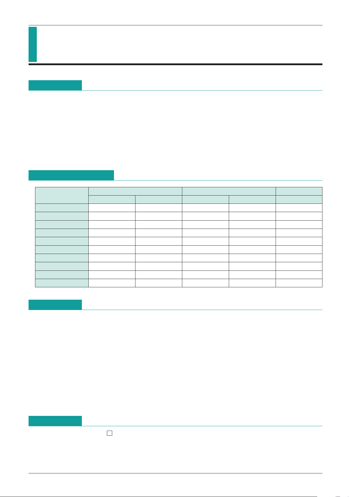
Model name
Overcharge protection Overdischarge protection Overcurrent
Detection voltage
Hysteresis
Detection voltage
Hysteresis
Detection voltage
MM1302A 4.25±0.05V 10mV 2.3V±0.1V 700mV 220±20mV
MM1292C 4.25±0.05V 200mV 2.4V±0.1V 600mV 150±15mV
MM1292D 4.35±0.05V 200mV 2.4V±0.1V 600mV 150±15mV
MM1302E 4.10±0.05V 10mV 2.4V±0.1V 600mV 150±15mV
MM1302F 4.35±0.05V 10mV None None
MM1302G 4.215±35V 10mV 2.3V±0.1V 700mV 220±20mV
MM1292H 4.30±0.05V 220mV 2.05V±0.1V 950mV 170±15mV
MM1292J 4.25±0.05V 220mV 2.4V±0.1V 600mV 150±15mV
MM1292K 4.25±0.05V 220mV 2.4V±0.1V 600mV 150±15mV
MM1292L 4.25±0.05V 220mV 2.2V±0.1V 800mV 100±10mV
Features
1. Current consumption (during overcharging) VCELL=4.5V 80µA typ.
2. Current consumption (normal) V
CELL=3.5V 13µA typ.
3. Current consumption (during excess discharging) V
CELL=1.9V 0.5µA typ.
4. Current consumption (during excess discharging) V
CELL=1.0V 0.1µA max.
5. Overcharge detection voltage (Ta=
-
20°C~+70°C)
4.25V±50mV (detection for each cell)
6. Hysteresis voltage
200mV±60mV (detection for each cell)
7. Excess discharge detection voltage 2.4V±0.1V (detection for each cell)
8. Discharge resumption voltage 3.0V±0.1V (detection for each cell)
9. Overcurrent detection voltage 150mV±15mV
10.Reset after overcurrent detection load release
11.Operating limit voltage 0.9V max.
Package
SOP-8C, SOP-8D(MM1292 F)
*
The box represents the rank resulting from the combination of protection functions.
Page 2
MITSUMI
Protection of Lithium Ion Batteries (two cells in series) MM1292
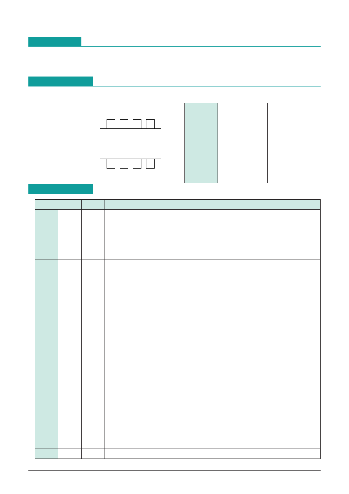
Pin Assignment
1432
8567
SOP-8C/SOP-8D
1 OC
2 GD
3 N.C
4 GND
5 TD
6 VL
7 CS
8 VH
Pin Description
Pin No.
Pin Output Function
1 OC Output
2 GD Output
3 DS Input
4 GND Input
5 TD Input
6 VL Input
7 CS Input
8 VH Input
Output pin for control of the charging control FET. When voltage detected between
VH-VL or VL-GND goes over overcharge detection voltage (VALM), the output PNP-
TR (open collector output) is switched ON, and charging is prohibited by activating
the element (NPN-TR, or N-ch FET) that switches the charging control FET to OFF.
This operation continues until the voltage falls below VALM.
Output pin for driving the discharge control FET. When voltage detected between VH-
VL and VL-GND goes over excess discharge voltage (VS), this pin goes H. When
voltage detected between VH-VL and VL-GND falls below VS and the voltage between
CS-GND is more than the voltage detected for an overcurrent (VCS), it goes L.
Input pin for discharge detection. When voltage between DS-GND during charge
detection exceeds discharge detection voltage (VDS), OC output is switched OFF
and charge control FET is switched ON.
Negative connection pin for the low side battery. It is also the GND pin for this IC.
(The IC's reference power supply pin.)
Over charge detection output non-induction time setting pin. The capacitor connected
between TD-GND is charged with constant current (ITC) during over charging. When
TC pin voltage exceeds the threshold value (VTC), OC output is switched ON.
Positive connection pin for the low side battery, and negative connection pin for the
high side battery.
Overcurrent detection pin during discharge, and charging detection pin during
power down. It detects discharge current using the source drain voltage (voltage
between CS-GND) of discharge control FET. Also, when the battery is charged with
a current whose CS-GND voltage after power down exceeds the start-up voltage
(VST), the bias current is drained to the interior circuit and operating status results.
Positive connection pin for the high side battery, and the IC's current input pin.
Applications
1. Cellular phones
2. Movies
Page 3
MITSUMI
Protection of Lithium Ion Batteries (two cells in series) MM1292
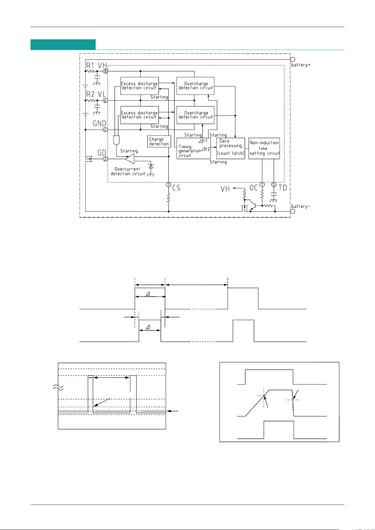
Block Diagram
Note 1. 45µA max. (current consumption during operation of overcharge detection section) flows to input
protection resistor R1.
Note 2. 0.3µA max. (when cells are balanced) flows to input protection resistor R2. When the cells are not
balanced, the current increases to wards correction.
Data intake
prohibition interval
Data intake prohibition interval
t2
t1
tOP
tST
Operating
interval
waiting interval
tOP
tST
Time
Average
current
30µA
5µA
Current
consumption
Current
consumption
Timing for setting non-induction time
V
CELL>4.25V
V
CELL<4.25V
Data processing
section
Non-induction
time
Overcharging
identification
Reset
VH
GC
VCS (battery-)
Page 4

MITSUMI
Protection of Lithium Ion Batteries (two cells in series) MM1292
Timing Chart
OC
TD
Overcharging identification
Data latch
Hold untill t (N+1)
Overcharging
detection output
operation starts
Start-up signal
generation timing
AND process
Discharging
state
GD
VL
VH
VS
VS
VS
V
ALM
V
ALM
V
ALM
V
ALM
V
ALM
operation stop
Discharging
prohibited
VS
unsettled (High impedance)
Current
consumption
OR
processing
Charging prohibited,
constant
current output
(source current)
unsettled
Absolute Maximum Ratings
Item Symbol Rating Units
Storage temperature T
STG
-
40~+125 °C
Operating temperature T
OPR
-
20~+70 °C
Power supply voltage V
OC max.
-
0.3~18 V
OC pin applied voltage V
OVOUT
-
10~VH V
CS pin applied voltage V
DCOUT
-
0.6~VH V
Allowable power dissipation Pd 300 mA
Page 5

MITSUMI
Protection of Lithium Ion Batteries (two cells in series) MM1292
Electrical Characteristics
(unless otherwise specified, Ta=25°C)
Item Symbol
Measurement Conditions
Min. Typ. Max. Units
Current consumption 1 I
VH1VCELL=4.5V, ROC=270kΩ 80 100 µA
Current consumption 2 I
VH2VCELL=3.5V (normal) 13.0 20.0 µA
Current consumption 3 I
VH3VCELL=1.9V (During excess discharge) 0.5 0.8 µA
Current consumption 4 I
VH4VCELL=1.0V (During excess discharge) 0.1 µA
VL pin input voltage I
VL VH=VL
-
0.3 0 0.3 µA
Overcurrent detection voltage V
ALM Ta=
-
20°C~70°C 4.20 4.25 4.30 V
Hysteresis voltage V
AL VAL=VALMH
-
VALML 140 200 260 mV
Overcharge detection voltage V
S 2.30 2.40 2.50 V
Discharge resumption voltage V
DF
Discharge resumed through voltage rise
2.90 3.00 3.10 V
Starting voltage V
ST Voltage applied between GND-CS pins
-
0.6-0.5 V
GD pin output voltage H V
GDH VCELL=3.5V, IL=10µA
VH-0.3 VH-0.2
V
GD pin output voltage L V
GDL VCELL=3.5V, IL=10µA, VCS=1V 0.2 0.3 V
OC pin output current I
OCH VCELL=4.5V 20 150 µA
Overcurrent detection voltage V
CS 135 150 165 mV
Reset by overcurrent load release
Overcurrent detection delay 1 T
OC11020mS
Overcurrent detection delay 2 T
OC2 between CS-GND pins > 0.8V 30 100 µS
Excess discharge detection delay
TOD 10 20 mS
TC pin charge current I
TC1 305080nA
TC pin threshold value V
TC
VCELL=4.5V, VTC=0 5V
V
OC=L H
3.65 3.90 4.15 V
Non-induction time for overcharge
TOC CTC=0.012µF 0.5 1.0 1.5 S
Operating limit voltage V
OPL 0.9 V
Note 1. For current consumption, it is assumed that high side cell voltage and low side cell voltage are
identical. When the cell voltages differ, it is set by the higher voltage.
2. GD pin are high impedance when the current consumption is below the operating limit voltage.
3. When the circuit configuration calls for discharge resumption through charging, the discharge
resumption voltage is 2.4V typ.
Description of Operation
[Outline]
This IC is used for protecting lithium ion batteries (two cell series connection type). Overcharge detection,
excess discharge detection, and overcurrent detection are built into each circuit. It controls the FET for
discharge control and charge control (external N-MOS FET). There are four major operating modes.
1. Overcharge mode
When the voltage between Vh-VI and VI-GND exceeds the overcharge voltage (V
ALM).
2. Normal mode
When the voltage between Vh-VI and VI-GND exceeds the excess discharge voltage (V
S) and is less
than the over charge voltage (V
ALM).
3. Excess discharge mode
When the voltage between Vh-VI and VI-GND is less than the excess discharge voltage (V
S).
4. Overcurrent mode
When the voltage between CS-GND is less than the overcurrent voltage (V
CS).
Page 6

MITSUMI
Protection of Lithium Ion Batteries (two cells in series) MM1292
[Operation]
1. Excess discharge detection circuit
The H cell excess discharge detection circuit monitors the voltage between VH-VL, while the L cell excess
discharge detection circuit monitors the voltage between VL-GND. When the voltage between VH-VL and VLGND exceeds VS, the operating state is maintained with bias current supplied from the bias circuit to the
delay circuit, the output control circuit, the overcurrent detection circuit, and the overcharge detection circuit.
When the battery current for either the H or L cell falls below VS, the current from the excess discharge
detection circuit to the bias circuit is switched off. Also, the capacitor connected to the delay circuit's
comparator (COD) input pin is charged using constant current. When this falls below the COD's reference
input potential, the bias current to output control and current to the bias circuit are switched off.
The excess discharge delay time (tOD) is set by the delay circuit and cannot be modified externally. When the
bias circuit is in waiting mode, the hysteresis loop to the excess discharge detection circuit is switched off,
and the detection voltage of the excess discharge detection circuit becomes discharge resumption voltage
(VDCH). When the battery is being charged and the voltage between CS-GND during excess discharge mode
falls below VST, however, start-up current is supplied to the bias circuit, and the hysteresis loop of the excess
discharge detection circuit is connected. Therefore, the excess discharge detection circuit detection voltage
becomes VS. Also, the overcharging detection circuit goes into waiting mode, so overcharging detection does
not occur in overcharging mode.
When the cell voltage of either the H or L cell exceeds V
ALM (one is excess discharging and the other is
overcharging), the bias current is maintained in the overcharging detection circuit. Therefore, the overcharging
is maintained until the current falls below V
ALM.
The timing (clock) for the waiting interval and operating interval is created by the timing generation circuit. In
normal mode, the only blocks operating during the waiting interval are the input stages for the timing
generation circuit and the data intake section. Other blocks operate only during the operation interval.
The operation interval and the waiting interval are set at a ratio of 1:10, reducing power consumption. The
voltage detection resistance of the overcharge detection circuit is switched on and off by the detection
section's SW circuit. Therefore, current does not flow to detection resistors during waiting time, resulting in
low current consumption during excess discharge mode.
(Operating sequence)
Bias current is supplied to the timing generation circuit and data intake section by the bias circuit of the
excess discharge detection section during normal mode.
The operation interval and the waiting interval are created by the timing generation circuit. During the
operation interval, bias current is supplied to the excess charging detection circuit, and cell voltages of both
the H and L cells are monitored.
2. Overcharging Detection Circuit
Page 7

MITSUMI
Protection of Lithium Ion Batteries (two cells in series) MM1292
CS-GND Voltage Mode Delay Time
Below V
CS Normal Mode
-
VCS~VF
Overcurrent Mode (Normal)
tOC1
Above VF
Overcurrent Mode (Short)
tOC2
(VF : Voltage between built-in NPN-TR and base emitter)
When the cell voltage of either the H or L cell exceeds V
ALM, an overcharge detection signal is output to the
data intake section, and a reset signal is prohibited from going to the data processing section.
When more than two consecutive clocks of the excess charging detection signal are input to the data intake
section, a determination is made that the overcharging detection signal has been properly input, and it is
output to the next stage. This prevents noise and mistaken determinations of overcharging caused by excess
cell voltage fluctuation.
When the date intake section outputs the overcharging detection signal, the data charge section goes into
operation. When more than two clocks of overcharging signals are input, this activates the latch on the
overcharging signal.
When the overcharging signal latch in the date latch section is activated, the next non-induction time circuit
goes into operation. When this operates, the TD pin is charged by constant current (ITC). The TD pin potential
and the threshold value (VTC) are compared by the non-induction time circuit comparator. When TD pin
voltage exceeds VTC, the OC pin output stage becomes operable and OC pin output PNP-TR (open collector)
is switched on. Also, bias current is supplied to the timing generation circuit and the operation of the
overcharging detection circuit is maintained.
When discharge occurs during overcharge mode (GND < DS pin), the discharge detection circuit charges the
TD pin and non-induction time is reset.
When cell voltage falls below V
ALM and the overcharging detection circuit signal is off, the reset prohibition is
lifted. The reset signal is sent to the data intake and data latch sections and the non-induction time circuit,
and normal mode is reinstated.
A diode is built in between the OC pin and GND. When OC pin potential falls below GND terminal VF, current
flows from the OC pin.
Therefore, when battery pack voltage <<charging voltage (charging device), charging is immediately
prohibited. (Generation conditions for the above mode vary depending on the external constant.)
3. Overcurrent Detection Circuit
The overcurrent detection circuit operates during overcharging. Load current detects current flowing on FET
equivalently, by monitoring the voltage between discharge control FET drain sources using the voltage
between CS-GND. (Monitoring of voltage drop using FET ON resistor load current.)
There are two modes for overcurrent detection : the normal mode and the short mode.
In normal mode, when voltage between CS-GND is equal to that between V
CS-Vf, overcharging detection
output at this time is input to the internal delay circuit. When overcurrent detection continues for longer than
overcurrent delay time 1 (tOC1), overcurrent mode is activated, and GD pin output goes L. (Discharge control
FET ON)
In short mode, when the voltage between CS-GND exceeds VF, the overcurrent mode operates without going
through the delay circuit. The delay time is determined by the internal circuit operating speed (Overcurrent
delay time 2 [tOC2], so the flow of overcurrent to the discharge control FET is for a short duration, limiting
stress on the FET.)
The VF has a temperature factor of-2mV/(C, so the switching level between normal and short mode varies
with the ambient temperature.
The overcurrent detection voltage (V
CS) is fixed, so the current value for overcurrent detection changes
according to discharge control FET ON resistance. Therefore, select an FET that conforms to the detection
current. FET ON resistance is highly sensitive to temperature, due to overcurrent detection voltage, and the
detection current changes due to FET heat emission resulting from ambient temperature and load current. In
addition, users should be aware that FET ON resistance also changes due to the voltage between FET gate
sources. (ON resistance rises when the voltage between gate sources falls.)
Load release resets from overcurrent mode.
 Loading...