

Page 1
MITSUMI
Protection of Lithium Ion Batteries (one cell) MM1301
Protection of Lithium Ion Batteries (one cell)
Monolithic IC MM1301
Outline
This IC provides protection for the MM1291 series of compact, high-precision type lithium ion batteries which
have been in use for some time. Precision of ±30mV is guaranteed between 0°C and +50°C, and this IC can
be used in applications where precision is crucial.
Features
1 Overcharge detection voltage Ta=0~+50°C VCEL±30mV
2 Overcharge detection delay time C
TD=0.082µF 1.0S typ.
3 Current consumption (normal operation V
CEL=3.5V) 10µA typ.
4 Current consumption (overdischarge operation V
CEL=1.9V) 0.7µA typ.
5 Overcurrent cancel conditions Load removed : Load of 5MΩ or greater across battery pack terminals
Package
VSOP-8A
Applications
Lithium ion battery pack (for battery protection)
1-Cell Protection ICs
Package
Overcharge
Overdischarge
Release Overcurrent detection
detection
Hysteresis
Dead time
detection voltage
Delay
SOP-8 VSOP-8
voltage
Overcurrent Detec time shot-mode
MM1301 AW 4.27V 200mV 2.3V 2.9V 100mV 0.9V
BW 4.17V 100mV 2.3V 2.9V 100mV 0.9V
CW 4.18V 100mV 2.3V 2.9V 125mV 0.45V
DW 4.28V 220mV 2.3V 2.9V 50mV 0.45V
EF 4.20V 100mV 2.3V 2.9V 125mV 0.45V
FW 4.28V 100mV 2.3V 2.9V 50mV 0.45V
GW 4.18V 220mV 2.3V 2.9V 125mV 0.45V
HW 4.35V 220mV 2.3V 2.9V 50mV 0.45V
JW 4.20V 220mV 2.3V 2.9V 125mV 0.45V
at
Ctd=
0.082µF
min. 0.5S
typ. 1S
max. 1.5S
min. 5mS
typ. 10mS
max. 15mS
min. 5mS
typ. 10mS
max. 15mS
Note : Under open-load conditions, returns to normal mode from overcurrent mode.
(For MM1291A to G, J, M, 5MΩ or higher; for MM1291H, K, 50MΩ or higher)
Page 2
MITSUMI
Protection of Lithium Ion Batteries (one cell) MM1301
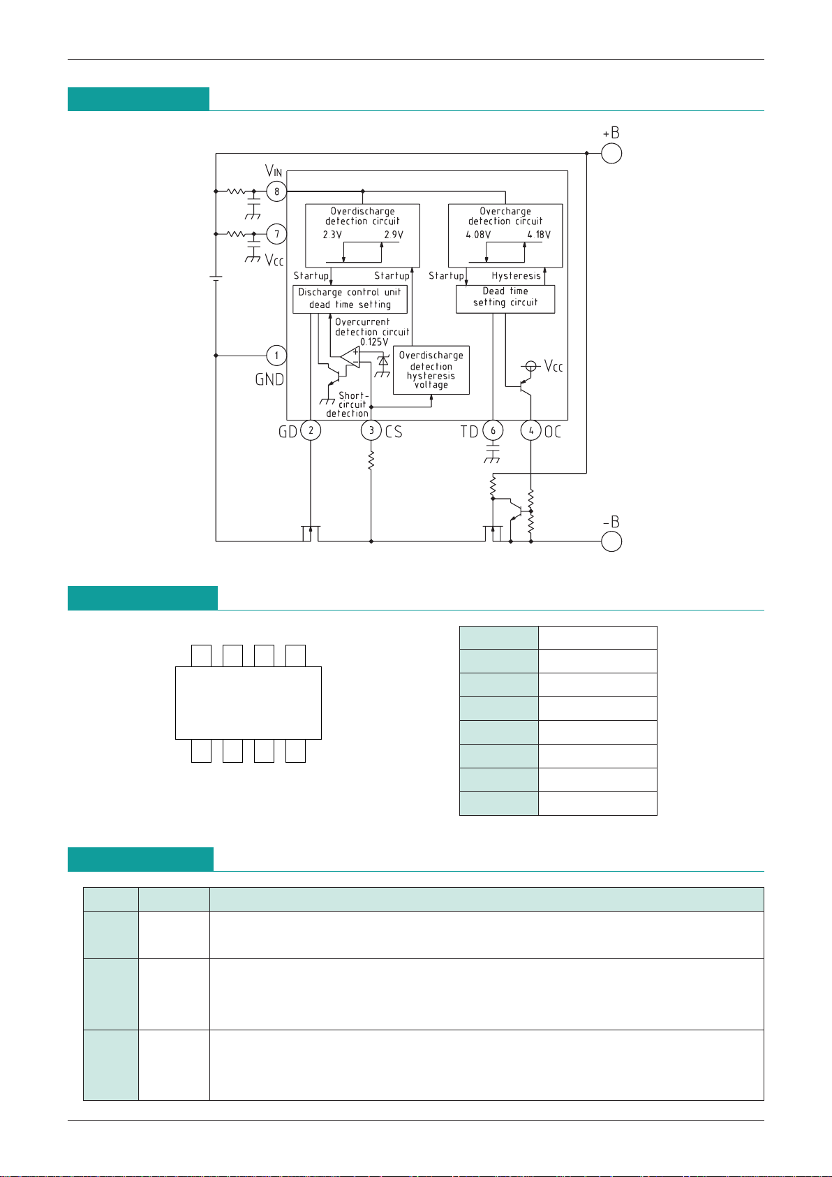
Pin Assignment
Pin Description
1432
8567
VSOP-8A
1 GND
2 GD
3 CS
4 OC
5 N.C
6 TD
7 V
CC
8 VIN
Pin No.
Pin name Function
1 GND
Negative power supply pin
Also serves as voltage detection pin for battery connected between V
IN and GND
Gate connection pin for discharge-control FET (N-ch)
2 GD Turns the gate off in overdischarge mode and overcurrent mode. Gate is turned on in
overcharge and normal modes.
Overcurrent detection input pin
3 CS Discharge current detected by connection to drain pin of discharge-control FET.
Discharge current = (CS-GND voltage)/(FET turn-on resistance)
Block Diagram
Page 3

MITSUMI
Protection of Lithium Ion Batteries (one cell) MM1301
Recommended Operating Conditions
Electrical Characteristics
(Except where noted otherwise, Ta=25°C)
Item Symbol Ratings Units
Operating temperature T
OPR
-
20~+70 °C
Operating voltage V
OP +0.9~+18 V
Item Symbol Measurement conditions Min. Typ. Max. Units
Overcharge detection voltage V
OC VCC=VIN=L H, Ta=0~50°C 4.15 4.18 4.21 V
Overcharge release voltage V
OCR VCC=VIN=H L 4.04 4.09 4.14 V
Overcharge sensing hysteresis
V
OCH=VOC
-
VOCR
VOCH 60 90 120 mV
Overdischarge detection voltage V
ODC1VCC=VIN=H L 2.20 2.30 2.40 V
Overdischarge release voltage V
ODR VCC=VIN=L H 2.78 2.90 3.02 V
Overcurrent detection threshold V
CS VCS=L H 112 125 138 mV
Overcurrent short-circuit detection V
CSS 0.35 0.45 0.55 V
Overcurrent release conditions
Load open : Load of 5MΩ or greater across battery pack terminals
Consumption current 1 (Normal mode)
(I
S1=ICC+IIN)
I
S1VCC=VIN=3.5V 10.0 14.0 µA
Consumption current 2 (Overdischarge mode)
IS2VCC=VIN=1.9V 0.7 1.0 µA
Absolute Maximun Ratings
(Ta=25°C)
Item Symbol Ratings Units
Storage temperature T
STG
-
40~+125 °C
Operating temperature T
OPR
-
20~+70 °C
Power supply voltage V
CC max.
-
0.3~+18 V
OC pin voltage V
OC max.
CS pin voltage V
CS max.
-
0.6~VCC V
Allowable loss Pd 300 mW
4 OC
Overcharge detection output pin
On overcharge, an external transistor is driven to turn off the charge-control FET (N-ch)
5 N.C
6 TD Overcharge detection dead time setting pin
7 V
CC Positive power supply voltage pin
8 V
IN Voltage detection pin for battery connected between VIN and GND
Notes : Overcharge mode : Battery voltage > overcharge detection voltage
Normal mode : Overdischarge detection voltage < battery voltage < overcharge detection voltage,
discharge current < overcurrent detection level
Overdischarge mode : Overdischarge detection voltage > battery voltage
Overcurrent mode : Discharge current > overdischarge detection level=CS-GND voltage > discharge
current turn-on resistance (discharge-control FET)
Page 4

MITSUMI
Protection of Lithium Ion Batteries (one cell) MM1301
Timing Chart
Overcharge cutoff voltage Overcharge expulsion voltage
Overdischarge expulsion voltage
Overdischarge cutoff voltage
removing load
Cell voltage
TD
FET gate (charge control)
FET gate (discharge control)
Normal mode Normal mode Normal mode
Overcurrent
Overcharge mode
*
1: The overcurrent short mode delay time (overcurrent delay time 2) is the response time of the IC itself.
In actual use, the time required for discharge of the gate capacitance of the discharge-controlling FET is
added to this.
When excessive currents cause considerable voltage fluctuation, the bias current within the IC may be
temporarily turned off, so that the response time is lengthened. The time constant of the capacitance and
resistance connected to the power supply pin should be set to at least 100µS/V, to limit power supply
fluctuations.
*
2: Use the following formula to calculate the overcharge detection time:
overcharge detection dead time t
OC = 12.2 CTD [S]
[where C
TD is the external capacitance in µF]
Overcurrent detection delay time 1 tCS1 5.0 10.0 15.0 mS
Overcurrent detection delay time 2 t
CS2
*
1 30 100 µS
Overdischarge detection delay time t
OD 5.0 10.0 15.0 mS
Overcharge detection delay time t
OC CTD=0.082µF
*
2 0.5 1.0 1.5 S
OC pin output current I
OC VCC=VIN=4.5V
-
30 µA
GD pin "H" Output voltage
V
GDH VCC=VIN=3.5V
V
CC VCC
V
(Normal mode)
-
0.3-0.1
GD pin "L" Output voltage
V
GDL1
V
CC=VIN=3.5V
(Overcurrent mode) V
CS=0.5V
0.1 0.3 V
GD pin "L" Output voltage
(Overdischarge mode)
V
GDL2VCC=VIN=1.5V 0.2 0.4 V
Page 5

MITSUMI
Protection of Lithium Ion Batteries (one cell) MM1301
Characteristics
50
40
30
20
10
0 1.0 2.0 3.0 4.0 5.0
ICC
IIN
Power supply voltage (ICC, VIN) (V)
Power supply current (ICC, IIN) (µA)
10
1
0.1
0.01
0.001 0.01 0.1
External capacitance (CTD) (µF)
Overcharge detection time (S)
Power supply current vs power supply voltage
Overcharge detection time
Application circuits
 Loading...