

Page 1
MITSUMI
Protection of Lithium Ion Batteries (three cells in series) MM1293
Protection of Lithium Ion Batteries (three cells in series)
Monolithic IC MM1293
Outline
This IC provides protection for lithium ion batteries in the event of overcharging, overdischarging and
overcurrents. When anomalies occur during charging or at other times and excessive voltages are applied,
after a certain time has elapsed for each cell an external FET switch is turned off (overcharging detection) ;
and in order to prevent overdischarge of the battery during discharge, when the voltage of individual batteries
falls below a fixed voltage, an external FET switch is turned off (overdischarging detection), and the IC is put
into low-consumption current mode. When large currents flow due to a short-circuit or other cause, an
external MOS switch is turned off (overcurrent detection).
Package
SSOP-16
Features
1. Current consumption (overcharging) VCELL > VCELLU 125µA typ.
2. Current consumption (normal operation) V
CELL < VALM 30µA typ.
3. Current consumption (overdischarge) V
CELL < VCELLS 0.1µA max.
4. Overcharge detection voltage (
-
20 to +70°C) VCELL : L H 4.25V±50mV/CELL
5. Overcharge hystereis voltage V
CELL : H L VCELLU
-
200mV/CELL typ.
6. Overcharge sensing dead time C=0.1µF 1.0S typ.
7. Overcharge sensing operation voltage V
CELL : L H 4.10V±150mV/CELL
8. Overdischarge detection voltage V
CELL : H L 2.40V/CELL typ.
9. Overdischarge sensing dead time C=0.1µF 1.0S typ.
10.Overcurrent detection voltage 0.15V typ.
11.Overcharge and overdischarve voltages as well as the overcurrent detection voltage can be changed upon
request.
Applications
Lithium ion battery pack for notebook computers
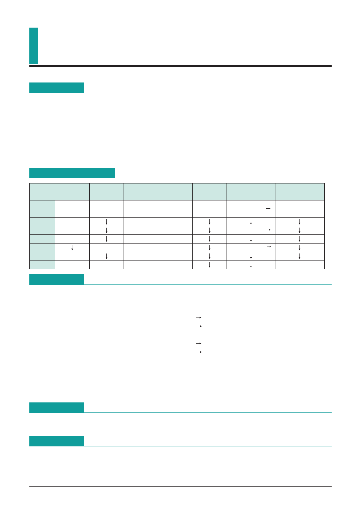
3-Cell Protection ICs
Rank
Overcharge Overcharge
Overdischarge Overdischarge
Overcurrent At overcurrent
Overcurrent release
detection voltage
hysteresis voltage
detection voltage
resume voltage detection voltage
detection conditions
A
4.35V±50mV
200mV typ. 2.35V typ. 3.05V typ.
150mV typ.
Pin 3 (DOHG pin) L H
Load release
250kΩ or more
B
4.25V±50mV
2.40V typ. 3.10V typ.
C
Same as rank A
Same as rank A
Pin 4 (OL pin) H L
D
Same as rank B
Same as rank B
E
none (several mV)
Same as rank B
Pin 3 (DOHG pin) L H
F
4.10V±50mV
2.35V typ. 3.00V typ.
G
Same as rank A
200mV typ.
Same as rank A Charging reset
Page 2
MITSUMI
Protection of Lithium Ion Batteries (three cells in series) MM1293
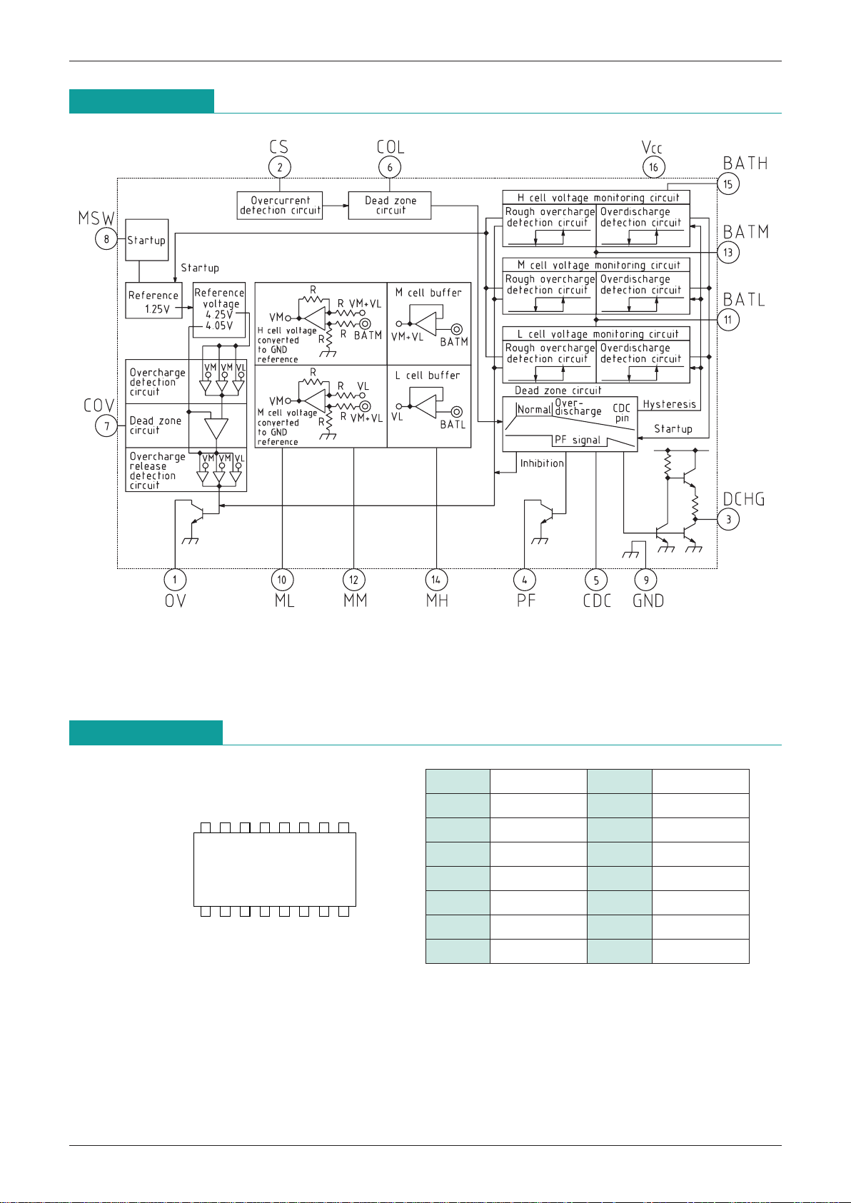
Block Diagram
Pin Assignment
SSOP-16
13 762458
16 13 1115 14 12910
1 OV 9 GND
2 CS 10 ML
3 DCHG 11 BATL
4 PF 12 MM
5 CDC 13 BATM
6 COL 14 MH
7 COV 15 BATH
8 MSW 16 V
CC
Page 3

MITSUMI
Protection of Lithium Ion Batteries (three cells in series) MM1293
Pin Assignment
Pin no. Pin name
Input/output
Function
1 OV Output
Overcharge detection output pin
NPN transistor open collector output; normally high impedance, goes to L
level on overdischarge
Overcurrent detection pin
Monitors equivalent load current through source-drain voltage drop of discharge-controlling
FET, and at or above the overcurrent detection voltage sets the DCHG pin to "H" and turns
off the discharge-controlling FET. Following overcurrent detection, current is passed from
this pin, and if the load is decreased, the overcurrent mode is canceled. Through this action
there is a temporary consumption current (at the V
CC
pin) of approx. 1 mA on resumption of
discharge and detection of overdischarge. This function is disabled in overdischarge mode.
2 CS Input
Pin driving the discharge-controlling FET (P-ch)
Normally "L"; on overdischarge set to "H"
Output pin for overdischarge detection signals
3 DCHG Output
Overdischarge detection pin
When the overdischarge detector detects overdischarge at the open collector output of
the NPN transistor, this pin is turned on. A delay is provided by setting a dead time until
discharge ends, so that by utilizing a reset or other signal from a CPU or some other
controlling device, the equipment can be put into standby mode.
4 PF Output
Pin to set the dead time for overdischarge detection
By connecting a capacitor between the CDC pin and GND, a dead time can be set.
Pin to set the dead time for overcurrent detection
5 CDC Input
6 COL Input
Pin to set the dead time for overcurrent detection
By connecting a capacitor between the COL pin and GND, a dead time can be
set. If NC, protection is triggered in a short amount of time; the dead time
should be set according to the application.
Pin to set the dead time for overcharge detection
By connecting a capacitor between the COV pin and GND, a dead time can be
set.
7 COV Input
8 MSW Input
Pin to switch the cell voltage monitor on/off
GND: monitor on, V
CC: monitor off
The cell voltage monitor converts the different cell voltages to a GNDreference voltage and outputs it from the ML, MM and MH pins.
9 GND Input
Ground pin
10 ML Output
Monitor output pin for the L cell voltage
11 BATL Input
Pin for input of L cell high-side voltage and M cell low-side voltage
12 MM Output
Monitor output pin for the M cell voltage
13 BATM Input
Pin for input of M cell high-side voltage and H cell low-side voltage
14 MH Output
Monitor output pin for the H cell voltage
15 BATH Input
Pin for input of H cell high-side voltage
16 VCC Input
Power supply input pin
The same potential as the BATH pin should be input
Absolute Maximun Ratings
(Ta=25°C)
Item Symbol Ratings Units
Storage temperature T
STG
-
40~+125 °C
Operating temperature T
OPR
-
20~+70 °C
Charge voltage V
BAT max. 18 V
Power supply voltage V
CC max. 18 V
Voltage applied to OV pin V
OV max. 18 V
Allowable loss Pd 300 mW
Page 4

MITSUMI
Protection of Lithium Ion Batteries (three cells in series) MM1293
Recommended Operating Conditions
Item Symbol Ratings Units
Operating temperature T
OPR
-
20~+70 °C
Operating voltage V
OPR +2~+18 V
Electrical Characteristics
(Except where noted otherwise, Ta=25°C, VCC=15V, V
CELL=VBATH=VBATM=VBATL
)
Item Symbol Measurement conditions Min. Typ. Max. Units
Consumption current (V
CC pin) 1 ICC1VCELL=4.4V 125 250 µA
Consumption current (V
CC pin) 2 ICC2VCELL=3.5V 30 60 µA
Consumption current (V
CC pin) 3 ICC3VCELL=2.2V 0.1 µA
Consumption current (BATH pin) 1
IBATH1VCELL=4.4V 11 22 µA
Consumption current (BATH pin) 2
IBATH2VCELL=3.5V 5 10 µA
Consumption current (BATH pin) 3
IBATH3VCELL=2.2V 2 4 µA
BATM pin input current 1 I
BATMVCELL=3.5V ±300 nA
BATM pin input current 2 I
BATMA VCELL=4.4V
-
0.6-0.3 0 µA
BATL pin input current 1 I
BATLVCELL=3.5V ±300 nA
BATL pin input current 2 I
BATLA VCELL=4.4V
-
0.6-0.3 0 µA
Overcharge detection voltage V
CELLU Ta=
-
20~+70°C, VCELL : 3.7V 4.5V 4.20 4.25 4.30 V
Overcharge detection
release voltage
V
CELLOVCELL : 4.5V 3.7V V
Overcharge sensing dead time t
OV COV=0.1µF 0.5 1.0 1.5 S
Overcharge sensing operation voltage
VALM VCELL : 3.5V 4.4V 3.95 4.10 4.25 V
Overdischarge sensing hysteresis voltage
VALM VCELL : 4.4V 3.5V 120 200 300 mV
Overdischarge detection voltage V
CELLSVCELL : 3.5V 2.0V 2.30 2.40 2.50 V
Discharge resume voltage V
CELLDVCELL : 2.0V 3.5V 2.95 3.10 3.25 V
Overdischarge sensing hysteresis voltage
VCSDVCELLD-VCELLS 490 700 910 mV
Overdischarge sensing dead time
tCDC1CCDC=0.1µF 0.5 1.0 1.5 S
Overdischarge reset dead time t
CDC2CCDC=0.1µF, VCS=VCC+0.3V 7 mS
Overcurrent detection voltage V
OC VCC
-
VCS, DCHG 0.135 0.150 0.165 V
Overcurrent sensing dead time t
COL1CCOL=0.001µF, DCHG 51015mS
Overcurrent reset dead time t
COL2CCOL=0.001µF, DCHG 51015mS
Overcurrent sensing delay time t
COL3CCOL=0, DCHG 150 µS
Overcurrent reset delay time t
COL4CCOL=0, DCHG 150 µS
Overcurrent protection release
Open-load condition 250kΩ
DCHG pin source current ISODCH
V
CELL
< V
CELL
S, SW1 : A, V
DCHG=VCC
-
1.8V
20 µA
DCHG pin sync current I
SIDCH VCELL > VCELLS, SW1 : A, VDCHG=0.8V 20 µA
DCHG pin output voltage H V
THDCHVCC
-
VDCHG, ISO=20µA, SW1 : B 1.8 V
DCHG pin output voltage L V
THDCLVDCHG
-
GND, ISI=-20µA, SW1 : B 0.8 V
OV pin sync current I
SIOV VOV=0.4V, Ta=
-
20~+70°C 0.2 mA
PF pin sync current I
SIPF VPF=0.4V, Ta=
-
20~+70°C 10 µA
V
CELL
U
-
260mV
V
CELL
U
-
200mV
V
CELL
U
-
140mV
Page 5

MITSUMI
Protection of Lithium Ion Batteries (three cells in series) MM1293
Timing Chart
Overcharge state
Sensing dead zone
t
OV
Normal state
Overcharge detection voltage
Cell voltage
COV pin
Pin OV
(pulled up)
Charging off
Overcharge detection cancel voltage
Cell voltage
CDC pin
DCHG pin
Pin PF
Discharge off
Reset dead zone
Overdischarge state Normal state
t
CDC1tCDC2
Discharge resume voltage
(pulled up)
Overdischarge detection voltage
Sensing dead zone
CS pin
COL pin
DCHG pin
Normal state Normal stateOvercurrent state
Reset dead zoneSensing dead zone
Current passed
from pin CS
Load released
t
COL tCOL
Overcharge
Overdischarge
Overcurrent
Page 6

MITSUMI
Protection of Lithium Ion Batteries (three cells in series) MM1293
Application circuits
Characteristics
Capacitance C (F)
1
100m
10m
1m
100P 1000P 0.01µ 0.1µ
Dead time t (s)
Overcharge, overdischarge sensing dead time
Capacitance C (F)
10m
100m
1m
10P 100P 0.001µ 0.01µ
Dead time t (s)
Overcurrent dead time
Note : The above characteristics are representative and are not guaranteed.
 Loading...