

Page 1

MITSUMI
TFT Liquid Crystal Interface
Monolithic IC MM1288CQ
Outline
TFT Liquid Crystal Interface MM1288CQ
This IC was developed as an interface IC for video equipment having a small monitor. This IC performs
correction and polarity identification to convert RGB signals into TFT liquid crystal RGB signals. A common
inversion circuit and sync separation circuit are built-in.
Features
1. Power supply voltage +13V, 0V or +5V, -8V
2. Built-in polarity ID circuit
3. Built-in γ correction circuit
4. Common inversion circuit built-in
5. 2 input switch built-in
6. Built-in contrast adjustment circuit
7. Built-in sync separation circuit
Package
QFP-48A
Applications
1. Navigation systems
2. Pachinko games (models with color TFT)
3. Videophones, conferencing systems
4. Game equipment
5. Others
γ
Page 2
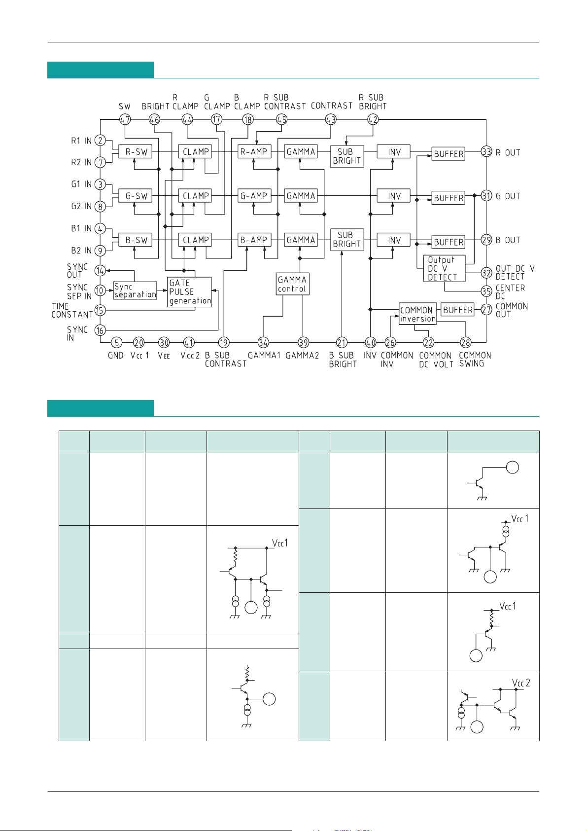
MITSUMI
Block Diagram
TFT Liquid Crystal Interface MM1288CQ
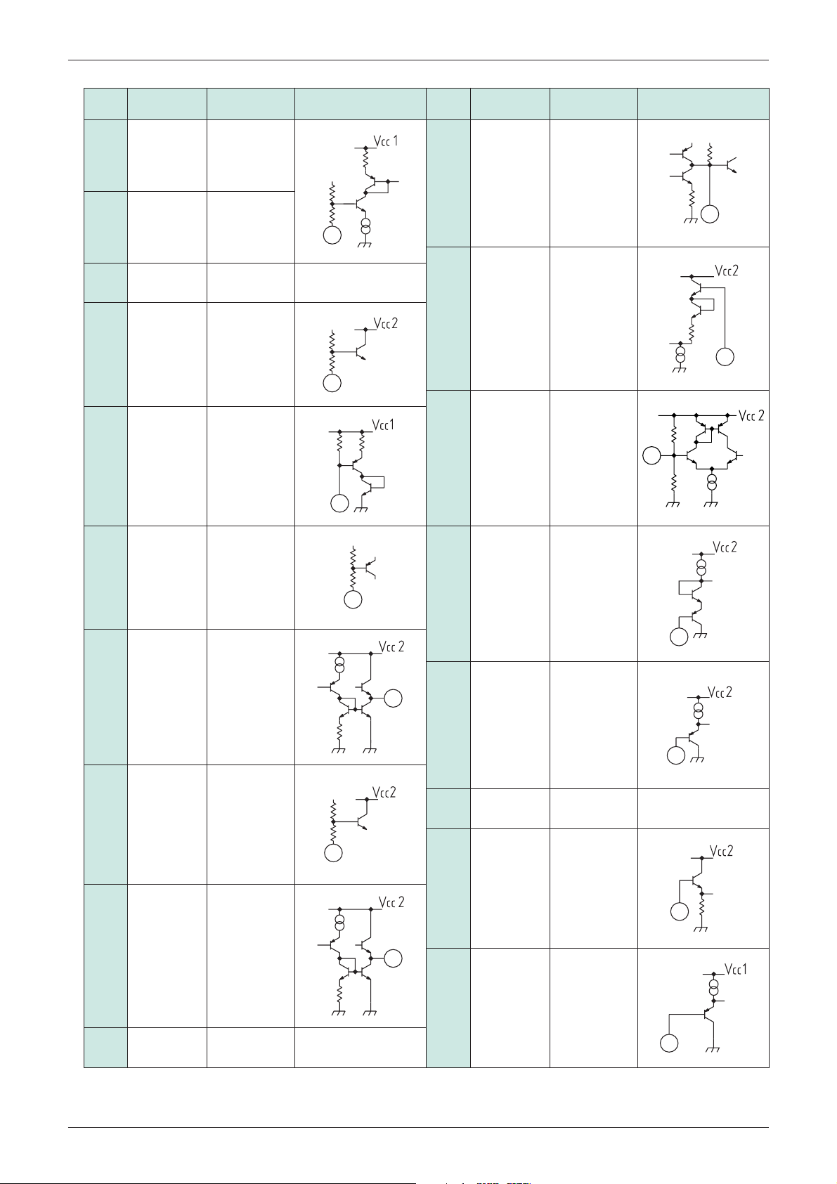
Pin Description
Pin no.
1, 6
11, 12
13, 23 NC
24, 25
36, 37
38, 48
2, 3
4, 7 RGB IN
8, 9
Pin name Function
5 GND GND pin
10
SYNC SEP IN
RGB input
Sync separation
input
Internal equivalent
circuit diagram
Pin no.
17, 18 CLAMP
Pin name Function
14
SYNC
OUT
15
16 SYNC IN
44 (RGB)
TIME
CONSTANT
Internal equivalent
circuit diagram
Sync output
Sync integration
Sync input
Clamp
Page 3
MITSUMI
TFT Liquid Crystal Interface MM1288CQ
Pin no.
19, 45
21, 42
Pin name Function
CONTRAST
43
CONTRAST
20 VCC1
BRIGHT
COMMON
22
DC VOLT
SUB
SUB
Internal equivalent
Subcontrast
Contrast
Positive polarity
power supply pin 1
Sub bright
Common
operating
point adjustment
circuit diagram
Pin no.
Pin name Function
OUT DC V
32
DETECT detection
34 GAMMA1
CENTER DC
35
Internal equivalent
circuit diagram
G output
Gamma
correction 1
Adjust center
voltage
26
27
28
29, 31
33
COMMON
INV inversion
COMMON
OUT output
COMMON
SWING
RGB OUT RGB output
Common
Common
Common
amplitude
adjustment
39 GAMMA2
40 INV
41
46 BRIGHT Bright
VCC2
Gamma
correction 2
Inversion
Positive polarity
power supply pin 2
30 VEE
47 SW Switch
Negative
polarity pin
Page 4
MITSUMI
RGB input
Inversion pulse
Primary color
output
COMMON output
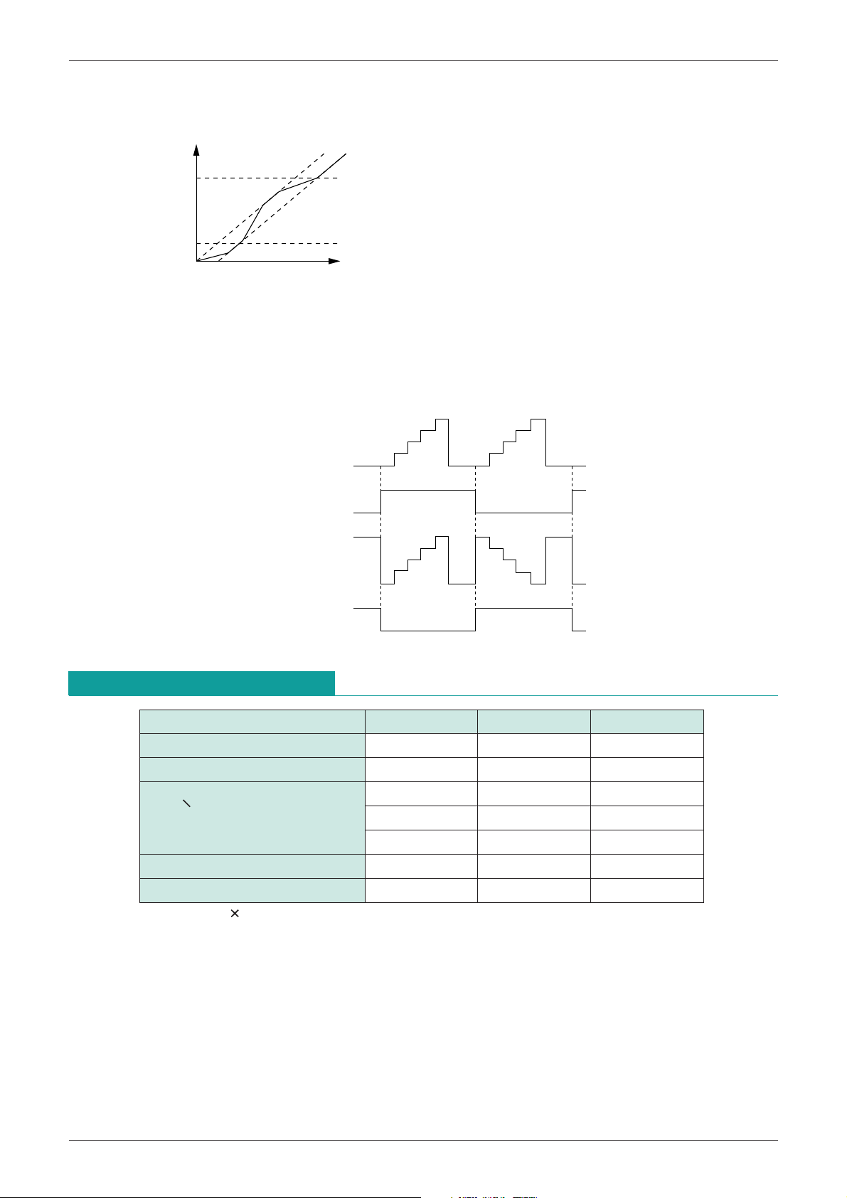
Note : GAMMA1, GAMMA2 (Pins 34, 39)
DC voltage applied to these pins sets γ correction DC voltage gain change point.
TFT Liquid Crystal Interface MM1288CQ
γ1
γ correction
Output is given characteristics as shown at left
according to LCD panel characteristics.
Output
γ2
Input
Pins 34 and 39 adjust the slope change position.
INV (40PIN)
The primary color output (pins 29, 31, 33) and COMMON output (pin 27) are inverted according to the
inversion pulse input to this pin. When COMMON INV (pin 26) has Vcc2 potential, the relationships between
the input, output and inversion pulse are as shown in the figure below.
Absolute Maximum Ratings
Item Symbol Ratings Units
Storage temperature T
Operating temperature T
Power supply voltage V
Allowable loss 1 Pd 1 500 mW
Allowable loss 2 Pd 2 1000
47mm 75mm 0.8mm printed circuit board (glass epoxy) board mounted.
*
(Ta=25°C)
V
STG
OPR
CC1
-
GND 6 V
CC2
-
VEE 15 V
GND
-
VEE 10 V
-
40~+125 °C
-
20~+85 °C
*
mW
Page 5

MITSUMI
TFT Liquid Crystal Interface MM1288CQ
Electrical Characteristics
Item Symbol Measurement conditions Min. Typ. Max. Units
V
CC1 pin operating power
supply voltage range
Operating power supply voltage
range when on power supply +2
Operating power supply voltage
range when on power supply ±
Consumption current 1 I
Consumption current 2 I
Voltage gain G
Voltage gain difference
between inputs
Reversed/non-reversed
voltage gain difference
RGB voltage gain
differences
Maximum voltage gain G
Minimum voltage gain G
Subcontrast change G
Input dynamic range V
Switch crosstalk C
VCC2+2 10.0 13.0 14.0 V
(Except where noted otherwise, Ta=25°C, All SW : A, VCC1=5.0V,
V
CC2=13V, GND=0V, VEE=0V, T16; SG1, T40; SG2, V46=3.5V)
V
CC1 4.5 5.0 5.5 V
VEE+2 GND V
VCC2± 4.5 5.0 5.5 V
VEE±
CC1VCC1=5V 8.5 15.0 mA
CC2VCC2=13V 17.0 22.0 mA
V 17 dB
Measure ratio of SG3 and
T29, 31, 33 sine waves.
-
8.5-8.0-6.5 V
Measure T29, 31, 33 sine
G
VSW 0.7 dB
SW2~4, 7~9 ;
B
G
VINV 0.7 dB
T2~4, 7~9 ;
SG3
Adjust V46
VRGB 0.7 dB
G
so that T29,
31 and 33
V max. 18 dB
amplitude is
8V.
wave ratio when SW47 :
B and V47=0V and 5V.
Measure T29, 31, 33 sine
wave ratio when T40=0V
and 5V.
Measure T29, 31, 33 sine
wave ratio.
SW43 ; B, V43=4.5V
Measure SG3 and T29,
31, 33 sine wave ratio.
SW43 ; B, V43=4.5V
V min. 13 dB
Measure SG3 and T29,
31, 33 sine wave ratio.
SW2~4, 19, 45 ; B, T2~4 ; SG3
Adjust V46 so that T29, 31 and 33
VSUB ±1 dB
amplitude is 8V. Measure ratio between
T29, 31 and T33 sine waves when V19
and 45 are 0.5~4.5V.
SW2~4, 43 ; B, T2~4 ; SG3, V43=1.5V
Adjust V46 so that T29, 31 and 33
INDR 1.5 1.9 VP-P
amplitude is 9V. Vary SG3 amplitude and
measure SG3 amplitude at the point
where T29, 31 and 33 signals start to be
saturated.
SW2~4, 43, 47 ; B, T2~4 ; SG4, V47=5V
Adjust V46 so that T29, 31 and 33
TSW
amplitude is 8V, and adjust V43 so that
T29, 31 and 33 sine wave amplitude is
5V
P-P. Vary SW47 in this state and
measure 1MHz spectrum change.
SW7~9, 43, 47 ; B, T7~9 ; SG4, V47=5V
-
50-44 dB
Adjust V46 so that T29, 31 and 33
amplitude is 8V, and adjust V43 so that
T29, 31 and 33 sine wave amplitude is
5V
P-P. Vary SW47 in this state and
-
50-44 dB
measure 1MHz spectrum change.
Page 6

MITSUMI
Item Symbol Measurement conditions Min. Typ. Max. Units
Crosstalk between RGB C
Output dynamic range (B-B)
Output dynamic range (B-W)
Output center voltage VC 6.3 6.5 6.7 V
Output center voltage change V
Bright change V
Amplitude difference between
bright RGB signals
Sub-bright change V
Frequency characteristic fmax. 4.0 5.0 MHz
COMMON output amplitude V
COMMON output maximum amplitude
COMMON output minimum amplitude
COMMON output center
maximum voltage
COMMON output center
minimum voltage
Sync separation input
sensitivity current
Sync separation output low voltage
Sync input threshold voltage V
Sync input input current I15
Subcontrast input current I18, I41
TFT Liquid Crystal Interface MM1288CQ
SW2 ; B T2 ; SG4
Adjust V46 so that T33 amplitude is 8V,
and adjust V43 so that T33 sine wave
TRGB
amplitude is 5V
P-P. Then measure the
-
48-40 dB
difference between T33 and T29, 31
signals 1MHz spectrum. Measure in the
same way for G B,R and B R, G.
VDR B
SW2~4 ; B, T2~4 ; SG4, V46=0.5V
-
B 10 11 VP-P
Measure T29, 31 and 33 signals.
SW2~4, 43 ; B, T2~4 ; SG4, V43=4.5V
VDR B
Adjust V46 so that T29, 31 and 33
-
W 6.0 7.0 VP-P
amplitude is 9V and measure T29, 31 and
33 sine wave amplitude.
Adjust V46 so that T29, 31 and 33 amplitude is
0V and measure T29, 31 and 33 DC voltage.
Adjust V46 so that T29, 31 and 33 amplitude
is 0V and measure the difference T29, 31 and
C 3.0 V
33 DC voltage when V35=5V and 8v
Measure the difference between T29, 31 and 33
BRIT 10.0 13.5 V
signal clamp levels when V46=0.5V and 4.5V.
VBRIT RGB
Adjust V46 so that T31 amplitude is 5.7V
and measure T29 and 33 amplitude ratio.
-
0.5 0.5 dB
After adjusting V46 so that T29, 31 and 33
amplitude is 6V, with SW21 and 42 : B, vary
V21 and 42 between 8~10V and measure
SUBB ±1 V
the maximum value of the difference
between T31 and T29, 33 amplitudes.
SW2~4, 29, 31, 33 ; B, T2~4 ; SG4
Adjust V46 so that T29, 31 and 33
amplitude is 8V, then adjust V43 so that
T29, 31 and 33 sine wave amplitude is
5V
P-P. Vary sine wave frequency at
measure cutoff frequency.
COM 6.0 6.5 VP-P
V
COM
V
COM
V
CO max. 8.5 V
V
CO min. 4.5 V
Measure T27 amplitude.
max.
SW28 ; B, V28=12V Measure T27 amplitude.
min.
SW28 ; B, V28=0V T27 amplitude.
SW22, 28 ; B, V22=5V, V28=0V
Measure T27 amplitude.
SW22, 28 ; B, V22=0.5V, V28=0V
Measure T27 DC voltage
8.0 VP
-
0.1 0 0.1 VP
Increase current flowing out on T10, and
measure outflow current when T14
IS
I
-
50-35-20 µA
voltage changes from high to low.
VSYNL 0.2 0.4 V
TH15 1.4 1.9 2.4 V
Measure T14 voltage when 5V is applied to T10.
Measure T14 inverted input voltage when
T16 voltage is changed from 0 5V.
SW16 ; B Apply 0V to T16 and measure I16.
-
1.5 µA
SW19, 45, 46 ; B
Measure I19 and 45 when V19 and 45 are
-
60 70 µA
0.5V and 4.5V.
-
P
-
P
Page 7

MITSUMI
TFT Liquid Crystal Interface MM1288CQ
Item Symbol Measurement conditions Min. Typ. Max. Units
Sub-bright input current I20, I38
COMMON DC VOLT input current
I21
SW21, 42, 46 ; B
Measure I21 and 42 when V21 and 42 are 7.5V and 10.5V.
SW22 ; B
Measure I22 when V22=0V.
-
50 40 µA
-
100 µA
SW26 ; B
COMMON INV threshold voltage
VTH24 6.0 6.5 7.0 V
Vary V26 between 0~13V and measure
V26 when T27 phase inverts.
COMMON INV input current I24
COMMON SWING input current I26
GAMMA1 input voltage I32 6 µA
GAMMA2 input voltage I35
INV threshold voltage V
TH36 2.5 3.0 3.5 V
INV input current I36
Contrast input current I39
Bright input current I42 3 µA
CENTER DC input current I35 105 110 165 µA
SW26 ; B
Measure I26 when V26=0 and 13V.
SW28 ; B
Measure I26 when V26=9 and 12V.
SW34 ; B
Measure I34 when V34=11V.
SW39 ; B
Measure I39 when V39=1V.
Vary T40 voltage from 0 5V and measure
the voltage when T27 phase inverts.
Measure I40 when V40 is 0V.
SW43 ; B
Measure I43 when V43 is 0.5V and 4.5V.
Measure I46 when V46=1.7V.
Measure I35 when V35=V
CC2
-
90 90 µA
-
60 60 µA
-
6µA
-
2µA
-
60 70 µA
SW2~4, 47 ; B, T2~4 ; SG3
Adjust V46 so that T29, 31 and 33
SW threshold voltage V
TH47 0.8 1.4 2.0 V
amplitude is 8V. Vary V47 voltage from
0 5V and measure V47 when T29, 31
and 33 sine waves disappear.
SW input current I43 4.5 µA
SW47 ; B Measure I47 when V47=0V.
SW2~4, 34, 43 ; B, T2~4 ; SG5
GAMMA1 fluctuation V34 0.8 1.2 2.1 V
Adjust V43 so that T29, 31 and 33 amplitude is
3V. Vary V34 voltage from 3 6V and measure
the amount of T29, 31 and 33 voltage change.
SW2, 3, 4, 39, 43 ; B, T2~4 ; SG5
GAMMA2 fluctuation V39 0.8 1.2 2.1 V
Adjust V43 so that T29, 31 and 33 amplitude is
3V. Vary V39 voltage from 6.2 8V and measure
the amount of T29, 31 and 33 voltage change.
H-to-L common transport delay time
L-to-H common transport delay time
COMMON fall time t
COMMON rise time t
Difference in COMMON
rise and fall times
tPHL 2µS
tPLH 2µS
THL 23µS
TLH 23µS
SW27, 28 ; B, T40 ; SG6
Adjust V28 so that T27 amplitude is 6V.
t
T
t
T= tTHL
-
tTLH
H-to-L primary color signal tPHL 2µS
transport delay time
L-to-H primary color signal
transport delay time
Primary color signal fall time t
Primary color signal rise time t
Difference in primary color
signal rise and fall times
t
PLH
THL 12µS
TLH 12µS
SW29, 31, 33 ; B, T40 ; SG6
Adjust V46 so that T29, 31 and 33
amplitude is 8V.
t
T 1µS
t
T= tTHL
-
tTLH
2µS
2µS
Page 8

MITSUMI
SG1
SG2
SG3
SG4
SG5
SG6
63.5US
(1H)
1.5US
10.9US
4.7US
3V
0V
3V
0V
0.5V
P-P
1VP
-
P
0.5VP
-
P
100kHz
1MHz
90%
10% 10%
90%
tr<50nS tf<50nS
5V
-
0V
VCC1VCC2VCC1
GND
V
EE
5V
13V
0V
-
8V
GND V
EE
VCC2
13V
13V
5V 5V
Left : +2
power supply
Impressed
power supply
Right : ± power supply
Example of Power Supply Use
Input Signal Waveforms
TFT Liquid Crystal Interface MM1288CQ
Page 9

MITSUMI
Measuring Circuit
TFT Liquid Crystal Interface MM1288CQ
Page 10

MITSUMI
Application Circuits
Basic Connection Diagram 1 (VCC1=5V, VCC2=13V)
TFT Liquid Crystal Interface MM1288CQ
Page 11

MITSUMI
Basic Connection Diagram 2 (VCC=5V, VEE=-8V)
TFT Liquid Crystal Interface MM1288CQ
 Loading...