

Page 1

MITSUMI
Hybrid Driver Monolithic IC MM1285
Hybrid Driver
Monolithic IC MM1285
This IC collects various driver functions used in pagers and other portable communication devices in a single
chip. Recently there have been requests for more compact pagers and portable telephones, and at the same
time new functions and features are being added, leading to a strong demand for miniaturized and hybrid
components. This IC meets these needs through adoption of a miniature package.
The speaker driver incorporates functions for varying audio volume through data, a feature which can be used in
novel applications.
Features
1. Configuration: Speaker driver,vibration motor driver, two LED drivers
2. The speaker driver is capable of varying the audio volume in four steps via parallel data
3. Power can be supplied by a single dry-cell battery
4. Low 0.1µA consumption current in standby mode
Package
TSOP-16A (MM1285XV)
Absolute Maximum Ratings
Item Symbol Ratings Units
Storage temperature T
STG
-
40~+125
°
C
Operating temperature T
OPR
-
10~+50
°
C
Power supply voltage V
CC max.
-
0.3~+6 V
Operating power supply voltage Vccop +1.0~+1.7 V
Voltage applied to output pin
OUT1~4
-
0.3~+15 V
OUT5
-
0.3~+5 V
Voltage applied to input pin
-
0.3~+5 V
Allowable loss Pd 300 mW
Outline
Page 2
MITSUMI
Hybrid Driver Monolithic IC MM1285
I/O Timing Chart
LED1
LED2
Vibrator
Speaker
Input
Output
Input
Output
Input
Output
Input
Output
SW1
SW2
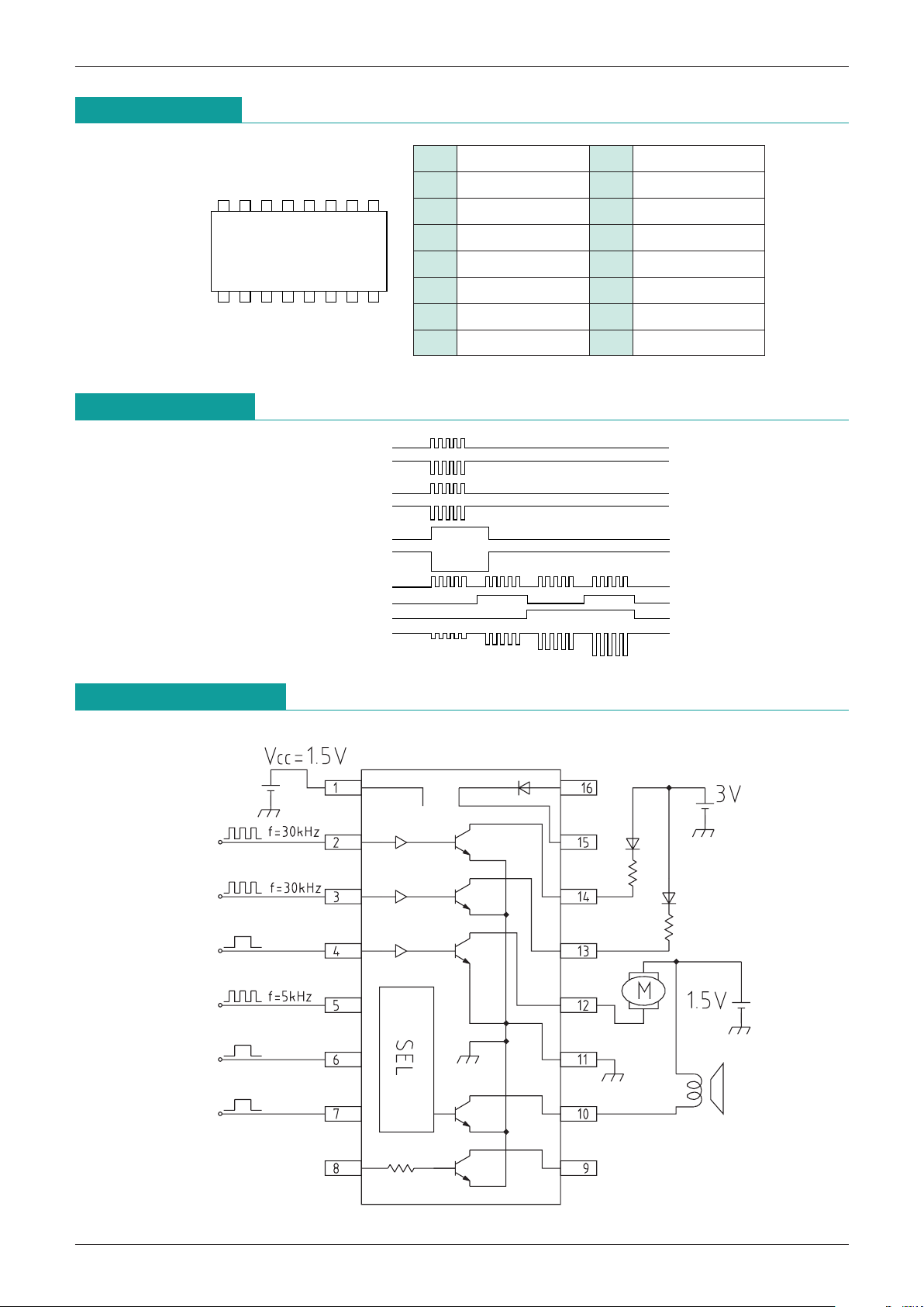
Application Circuits
Pin Assignment
13 762458
16 13 1115 14 12910
1 VCC 9 O5
2 I1 10 O4
3 I2 11 GND
4 I3 12 O3
5 I4 13 O2
6 S1 14 O1
7 S2 15 KATHODE
8 I5 16 ANODE
Page 3

MITSUMI
Hybrid Driver Monolithic IC MM1285
Electrical Characteristics
(Except where noted otherwise, Ta=25°C, VCC=1.5V)
Item Measurement conditions Min. Typ. Max. Units
Standby current All input pins=0V
--
0.1 µA
Consumption current A (O1 pin ON) I1=H, another pin=L 1.4 2.2 2.9 mA
Consumption current B (O2 pin ON) I2=H, another pin=L 1.4 2.2 2.9 mA
Consumption current C (O3 pin ON) I3=H, another pin=L 7.0 11.0 14.5 mA
Consumption current D (O4 pin ON) I4=H, S1=H, S2=H, another pin=L 7.0 11.0 14.5 mA
Consumption current E (O4 pin ON) I4=H, S1=H, S2=H, another pin=L 3.5 5.5 8.0 mA
Consumption current F (O4 pin ON) I4=H, S1=H, S2=H, another pin=L 1.1 1.6 2.2 mA
Consumption current G (O4 pin ON) I4=H, S1=H, S2=H, another pin=L 0.45 0.70 0.95 mA
Input threshold All input pins 0.40 0.65 0.85 V
Input resistance value
2
•3•4•5•6•
7 PIN
*
220k
Ω
I5pin (8PIN) only
*
10k
Ω
Input current
2
•3•4•5•6•
7 PIN, VIN=3V 8.3 11 16 µA
I5pin (8PIN) only, V
IN=3V 170 230 330 µA
Output resistance (O1 pin) I
O=20mA 5 10 Ω
Output resistance (O2 pin) I
O=20mA 5 10 Ω
Output resistance (O3 pin) I
O=180mA 1 1.5 Ω
Output resistance A (O4 pin) I
O=100mA, S1=H, S2=H 1 1.5 Ω
Output resistance B (O4 pin) I
O=50mA, S1=L, S2=H 7 10 13 Ω
Output resistance C (O4 pin) I
O=5mA, S1=H, S2=L 38.5 55 71.5 Ω
Output resistance D (O4 pin) I
O=1mA, S1=L, S2=L 154 220 280 Ω
Output current (O5 pin) V (I5) =1.5V, V (O5) =0.5V 2 10
-
mA
O5 pin acquisition current V (I5) =0V, V (O5) =5V
--
0.1 µA
O5 pin voltage V(I5)=0.85V, pulled up to 2V by 1MΩ
--
0.05 V
ON transport delay time A I1=L H
*
0.3
µS
OFF transport delay time A I1=H L
*
0.9
µS
ON transport delay time B I2=L H
*
0.3
µS
OFF transport delay time B I2=H L
*
0.9
µS
ON transport delay time C I3=L H
*
0.3
µS
OFF transport delay time C I3=H L
*
1.4
µS
ON transport delay time D I4=L H, S1=H, S2=H
*
0.5
µS
OFF transport delay time D I4=H L, S1=H, S2=H
*
1.0
µS
Diode forward voltage IF=3mA 0.65 0.70 0.75 V
Diode reverse leakage voltage VR=5.5V 10 µA
Notes.1: Asterisks (*) indicate design values.
2: Voltages applied to input pins are to be H=1V, L=0V.
 Loading...