

Page 1

MITSUMI
High-Precision Three-Pin Regulator MM1257
High-Precision Three-Pin Regulator
Monolithic IC MM1257
Outline
This IC is a high-precision high-voltage stabilized power supply device which stands out from ordinary lowsaturation three-pin regulators.
It can be used at a wide range of output voltages, from 3V to 12V, delivering output currents up to 100mA. It
is one of a series of devices available at lower prices than previous regulators.
Features
1. Input current 27V max.
2. Output noise voltage 200µV
RMS typ.
3. Maximum output current 100mA max.
4. No-load input current 500µA typ.
5. Thermal shutdown circuit provided
6. Output voltage ranks A : 12V±2% E : 6V±2%
B : 10V±2% F : 5V±2%
C : 9V±2% G : 3V±2%
D : 8V±2%
Package
TO-92A (MM1257 T)
MMP-4A (MM1257 M)
*
The output voltage rank appears in the boxes.
Applications
1. Handheld computers
2. Portable transceivers
3. Cordless phones
12
43
MMP-4A
123
TO-92A
Pin Assignment
1 NC
2 VIN
3 VOUT
4 GND
1 VOUT
2 GND
3 V
IN
Page 2
MITSUMI
High-Precision Three-Pin Regulator MM1257
Absolute Maximum Ratings
(Ta=25°C)
Item Symbol Ratings Units
Storage temperature T
STG
-
40~+125 °C
Operating temperature T
OPR
-
20~+75 °C
Power supply current V
CC max. 27 V
Output current I
OUT 100 mA
Maximum Ratings Pd
200 (MMP-4A), 300 (TO-92A)
mW
Recommended Operating Conditions
Item Symbol Ratings Units
Input voltage V
IN 7~27 V
Output current I
O 1~100 mA
Pin Description
Pin no. Pin name Function
1 N.C N.C
2 V
IN Power supply input pin
3 V
OUT Regulator output pin
4 GND GND
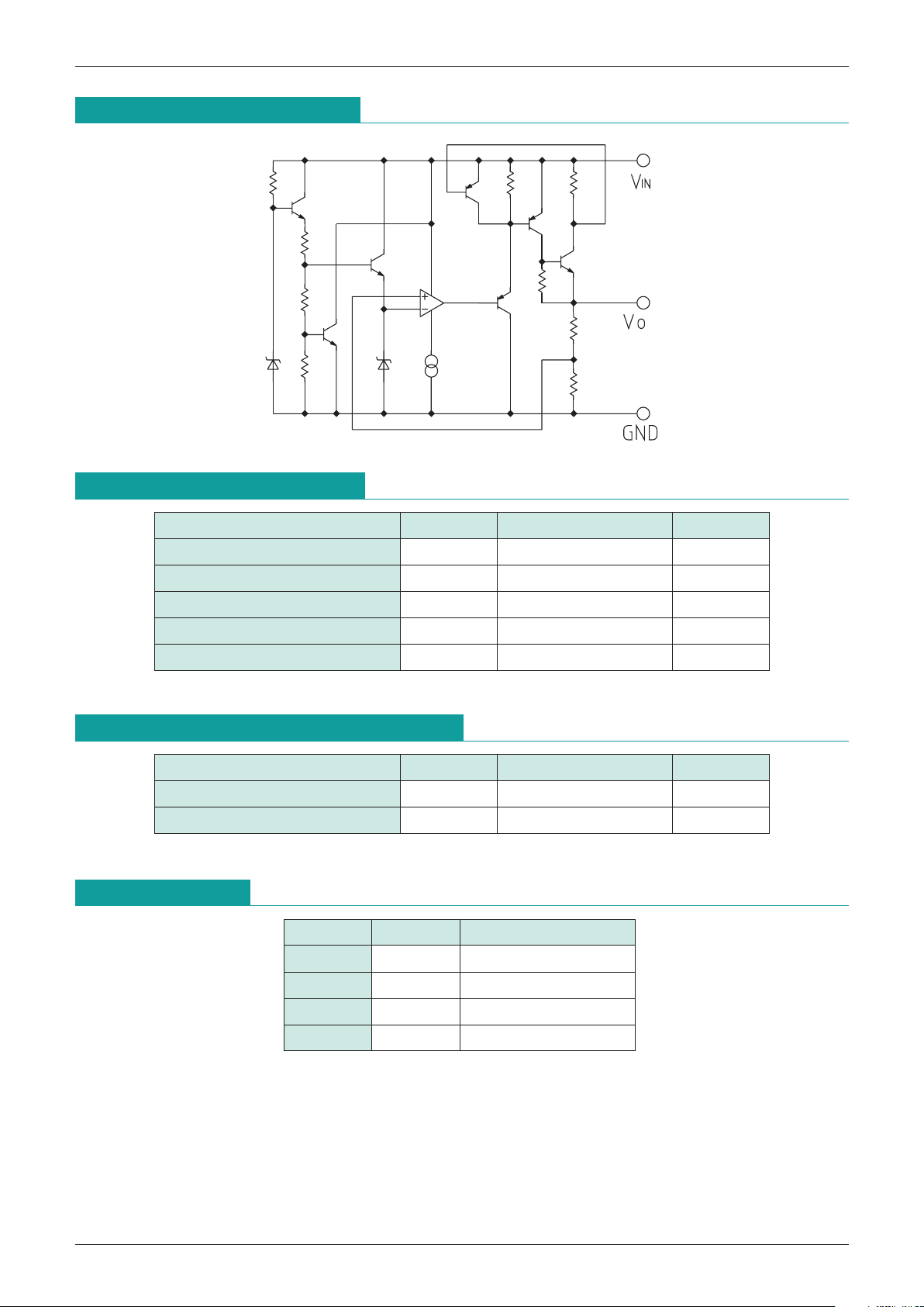
Equivalent Circuit Diagram
Page 3

MITSUMI
High-Precision Three-Pin Regulator MM1257
Measuring Circuit
Electrical Characteristics
(VO=5V)
Item Symbol
Measurement
Measurement
Min. Typ. Max. Units
circuit conditions
A 11.76 12.0 12.24
B 9.80 10.0 10.20
C 8.82 9.0 9.18
Output voltage V
O 1
VIN=Vo+3V, Io=40mA
D 7.84 8.0 8.16 V
E 5.88 6.0 6.12
F 4.90 5.0 5.10
V
IN=7V, Io=40mA G 2.94 3.0 3.06
No-load input current I
CCq1VIN
=Vo+4V, Io=40mA
0.50 1.50 mA
VIN=14.5V~25V, Io=40mA
A 120 250
VIN=12.5V~24V, Io=40mA
B 110 250
VIN=11.5V~22V, Io=40mA
C 100 250
Input fluctuation rate V1 1
VIN=10.5V~22V, Io=40mA
D 90 250 mV
VIN=8.5V~20V, Io=40mA
E 60 200
VIN=7V~20V, Io=40mA
F 50 150
VIN=7V~18V, Io=40mA
G 25 150
VIN=15V, Io=1~100mA
A 80 160
VIN=13V, Io=1~100mA
B 70 140
VIN=12V, Io=1~100mA
C 65 130
Load fluctuation rate V2 1
VIN=11V, Io=1~100mA
D 60 120 mV
VIN=9V, Io=1~100mA
E4080
VIN=8V, Io=1~100mA
F2060
VIN=8V, Io=1~100mA
G2060
Application Circuits
 Loading...