

Page 1
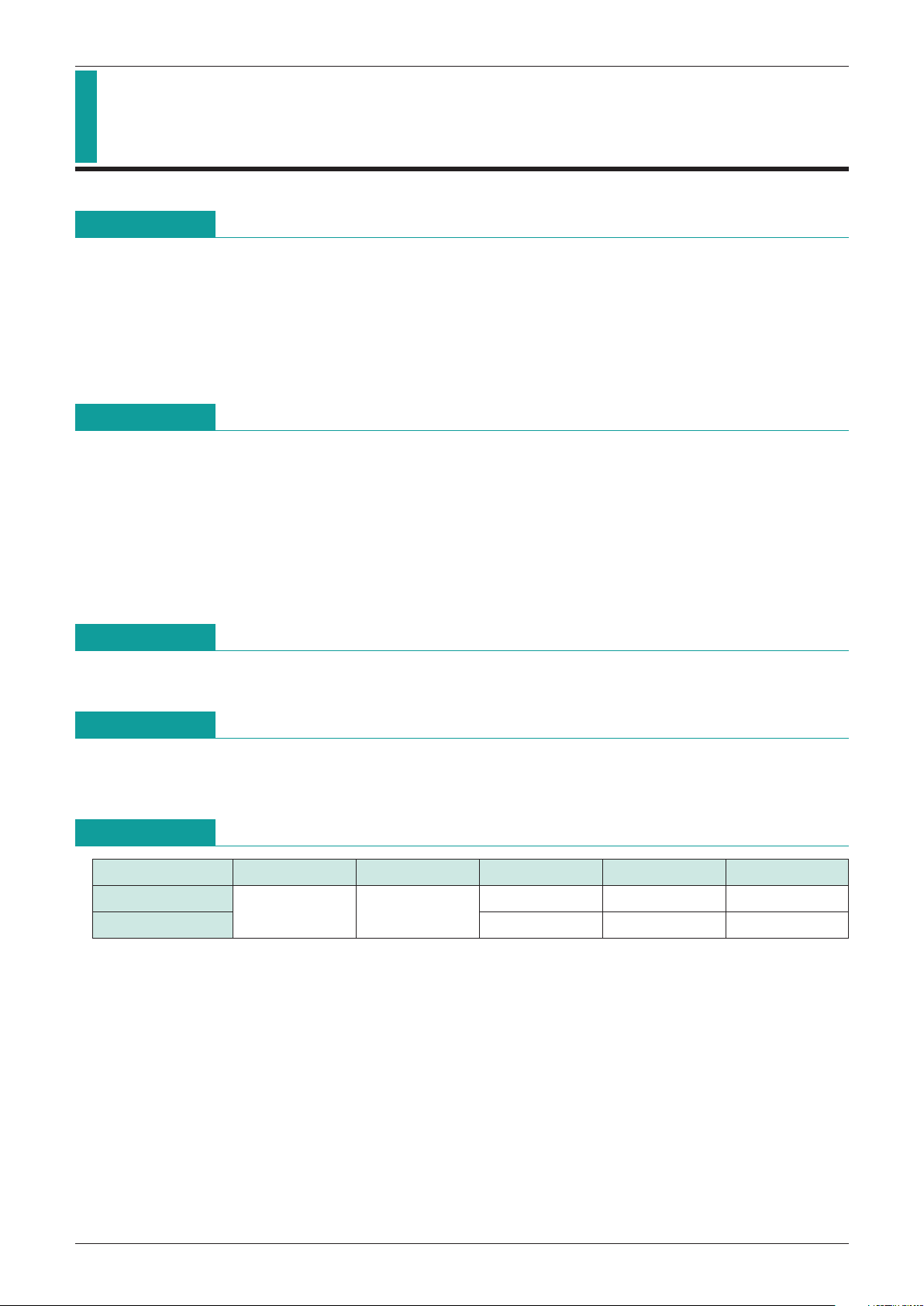
Model VSLB VSLR TPR TWD TWR
MM1135 100mS 10mS 2mS
MM1136
3.4V 3.2V
100mS 100mS 2mS
MITSUMI
System Reset (with built-in watchdog timer) MM1135, MM1136
System Reset (with built-in watchdog timer)
Monolithic IC MM1135, MM1136
Outline
These ICs were developed to drive low voltage batteries, and have a watchdog timer with built-in
microcomputer reset voltage detection circuit and low battery detection circuit.
A single reference voltage is used for low battery voltage detection and microcomputer reset voltage
detection, so detection voltage difference is uniform (.=.0.2V). Further, there is a built-in watchdog timer for
operation diagnosis, which prevents the system from running wild by generating an intermittent reset pulse
during system mis-operation.
Features
1. Accurate voltage drop detection voltage
1. Low battery detection 3.4V±3%
2. Power supply voltage detection 3.2V±3%
3. Detection voltage error 0.2V±20mV 1-2
4. Hysteresis Both 50mV typ.
2. Watchdog function stop pin (can be made to function only as reset IC during V
CC rise)
3. Low current consumption 150µA typ.
Package
SOP-8C (MM1135XF, MM1136XF)
Series Table
Applications
1. 3V cordless telephones
2. Various types of small, handy equipment
*
CT=0.02µF
T
PR : Reset hold time during VCC rise
T
WD : Timer monitoring time
T
WR : Reset time
V
SLB : Battery check detection voltage
V
SLR : Reset detection voltage
Page 2
MITSUMI
System Reset (with built-in watchdog timer) MM1135, MM1136
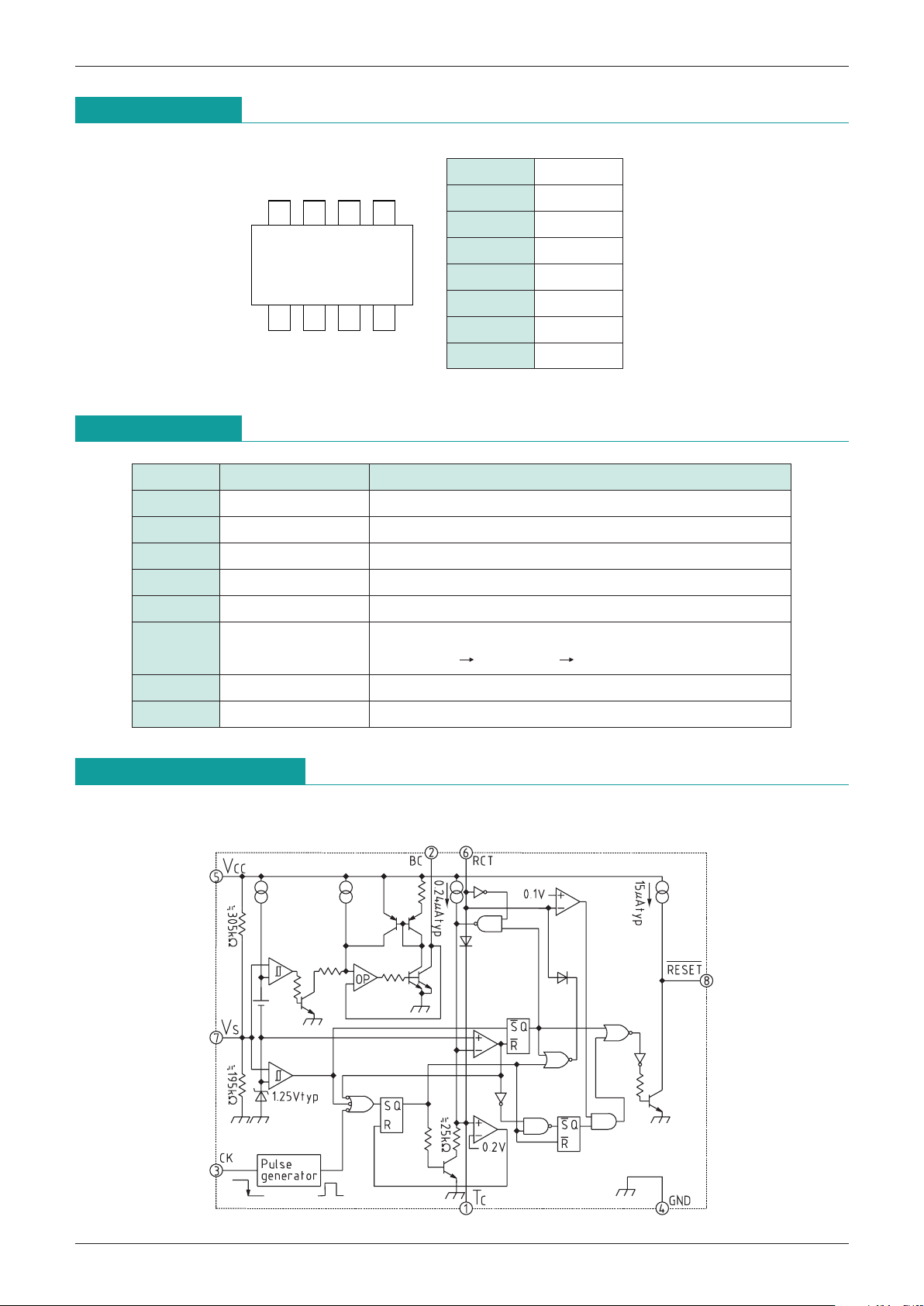
Pin Assignment
1432
8567
SOP-8C
1 TC
2
BC (RESET
----------------------------------------------------------------------------------------
)
3 CK
4 GND
5 V
CC
6 RCT
7 V
S
8
RESET
----------------------------------------------------------------------------------------
Pin Description
Pin No. Pin name Function
1 TC T
WD, TWR, TPR time setting pins.
2 BC (
RESET
----------------------------------------------------------------------------------------
) Battery check output pin (RESET low level output) for 3.4V
3 CK Clock input pin
4 GND GND pin
5 V
CC Power supply voltage input pin
6 RCT
Watchdog timer stop pin
Operation OPEN, Stop connect to GND
7 V
S Detection voltage fine adjustment pin
8
RESET
----------------------------------------------------------------------------------------
Reset output pin (low output)
Block Diagram
Page 3
MITSUMI
System Reset (with built-in watchdog timer) MM1135, MM1136
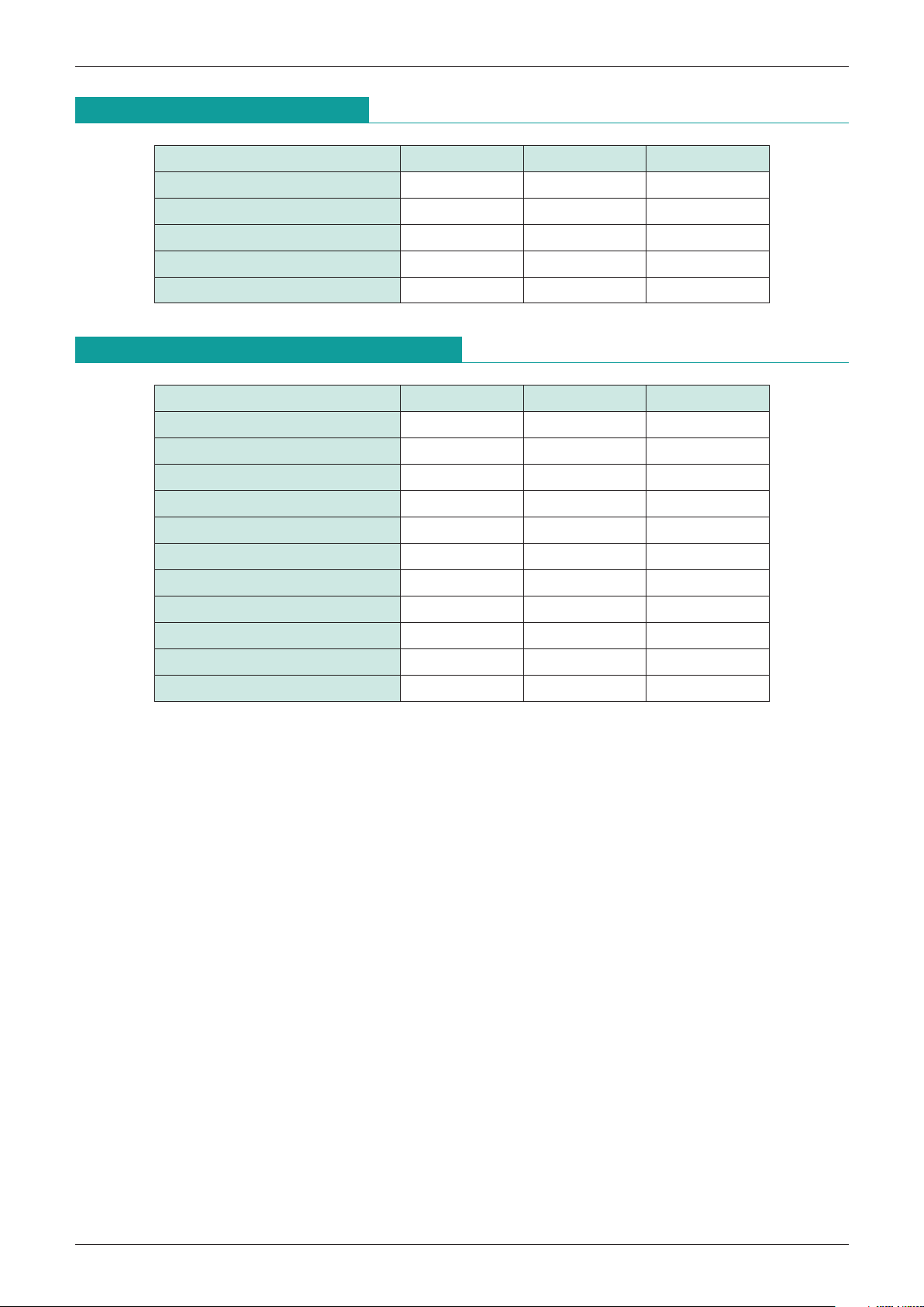
Absolute Maximum Ratings
Item Symbol Rating Units
Power supply voltage V
CC max.
-
0.3~+7 V
Voltage applied to input pin V
IN
-
0.3~VCC+0.3 (
<
=
+7)
V
Voltage applied to output pin V
OUT
-
0.3~VCC+0.3 (
<
=
+7)
V
Allowable loss Pd 450 mW
Storage temperature T
STG
-
40~+125
°
C
Recommended Operating Conditions
Item Symbol Rating Units
Power supply voltage V
CC +2.5~+6.5 V
RESET
--------------------------------------------------
sync current IOLR 0~1.5 mA
BC sync current I
OLC 0~1.5 mA
Clock input high level voltage V
CKH 1.4< V
Clock input low level voltage V
CKL <0.4 V
Clock monitoring time setting T
WD 1~1000 mS
Clock rise and fall times t
RCK, tFCK <100
µS
Power supply voltage rise times tRVCC 100< µS
Power supply voltage fall times t
FVCC 50< µS
TC pin capacitance C
T 0.002~2 µF
Operating temperature T
OP
-
25~+75 °C
Page 4
MITSUMI
System Reset (with built-in watchdog timer) MM1135, MM1136
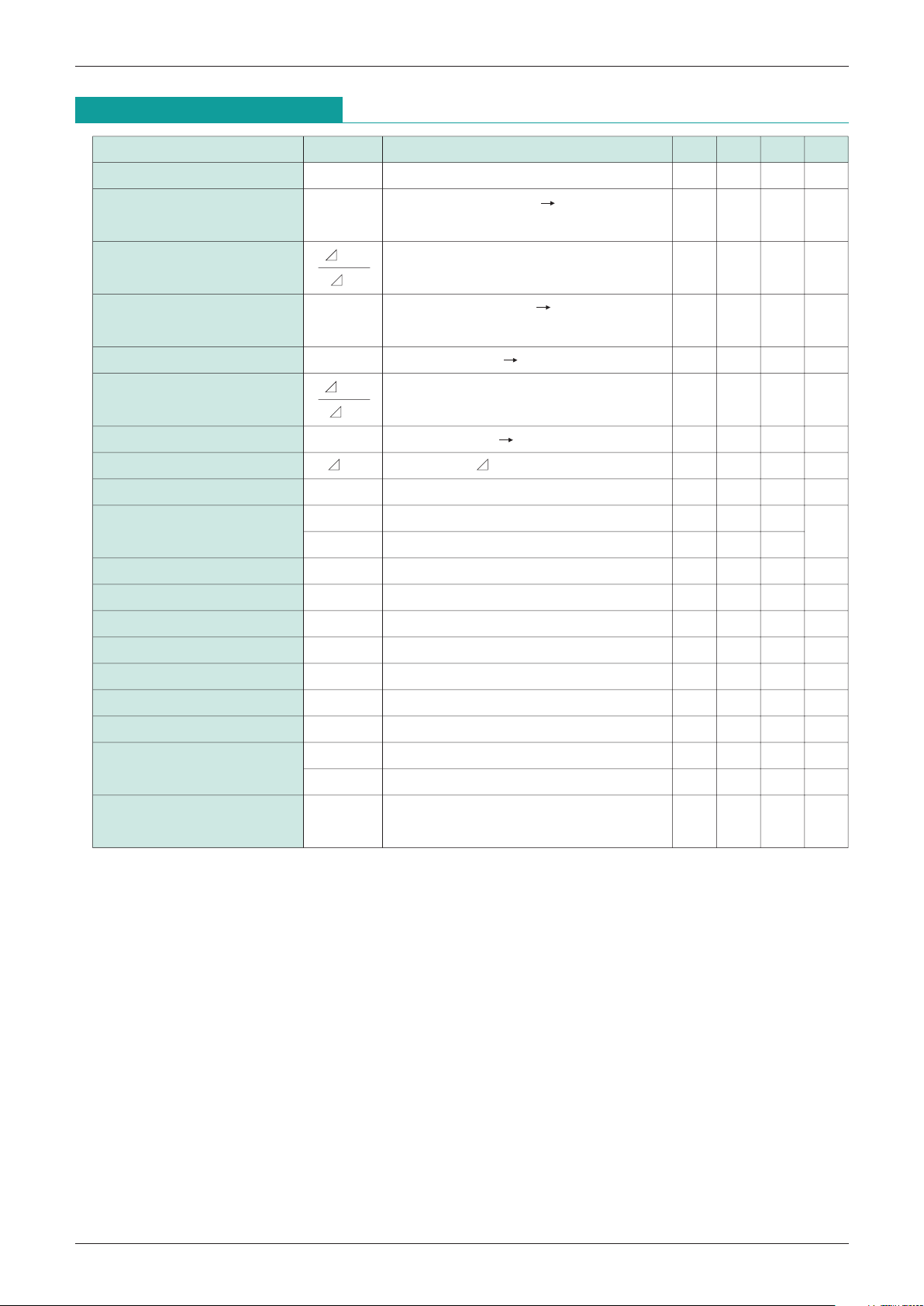
Electrical Characteristics
(Except where noted otherwise, Ta=25°C, Vcc=3.8V)
Item Symbol Measurement conditions Min. Typ. Max. Units
Consumption current I
CC No load 200 280 µA
RESET detection voltage V
SLR
VCC : High Low
RCT : GND, V
TC=OPEN
3.10 3.20 3.30 V
Detection voltage V
SR
±0.01 ±0.05 %/°C
temperature coefficient R T
Hysteresis voltage R V
HYSR
VCC : Low High
25 50 100 mV
RCT : GND, V
TC=OPEN
BC detection voltage V
SLB VCC : High Low, RLB=10kΩ 3.30 3.40 3.50 V
Detection voltage V
SB
±0.01 ±0.05 %/°C
temperature coefficient B T
Hysteresis voltage B V
HYSB VCC : Low High, RLB=10kΩ 25 50 100 mV
Detection voltage difference V
SL VSL=VSLB
-
VSLR 0.18 0.20 0.22 V
CK input threshold V
TH 0.8 1.2 2 V
CK input current
I
IH VCK=3.8V 0 1
µA
I
IL VCK=0.0V
-
15
-
6
-
2
Output voltage RH V
OHR IRESET
---------------------------------------------------
=-5µA 3.0 3.4 V
Output voltage BH V
OHB RLB=10kΩ 3.2 3.6 V
Output voltage RL V
OLR IRESET
---------------------------------------------------
=1mA, VCC=3.0V 0.3 0.5 V
Output voltage BL V
OLB IBC=5mA, VCC=3.0V 0.3 0.5 V
Output sync current R I
OLR VRESET
---------------------------------------------------
=0.5V, VCC=3.0V 1 2 mA
Output sync current B I
OLB VBC=0.5V, VCC=3.0V 5 10 mA
Output source current R I
OHR VRESET
---------------------------------------------------
=3.4V 8 15 µA
C
T charge current
I
CT1VTC=1.0V during watchdog timer operation
-
0.48-0.24-0.16
µA
I
CT2VTC=1.0V during power ON reset operation
-
0.48-0.24-0.16
µA
Minimum operating power supply
VRESET
---------------------------------------------------
=0.4V
voltage to ensure RESET
-----------------------------------------------
VCC
IRESET
---------------------------------------------------
=0.1mA
0.8 1.0 V
Page 5
MITSUMI
System Reset (with built-in watchdog timer) MM1135, MM1136
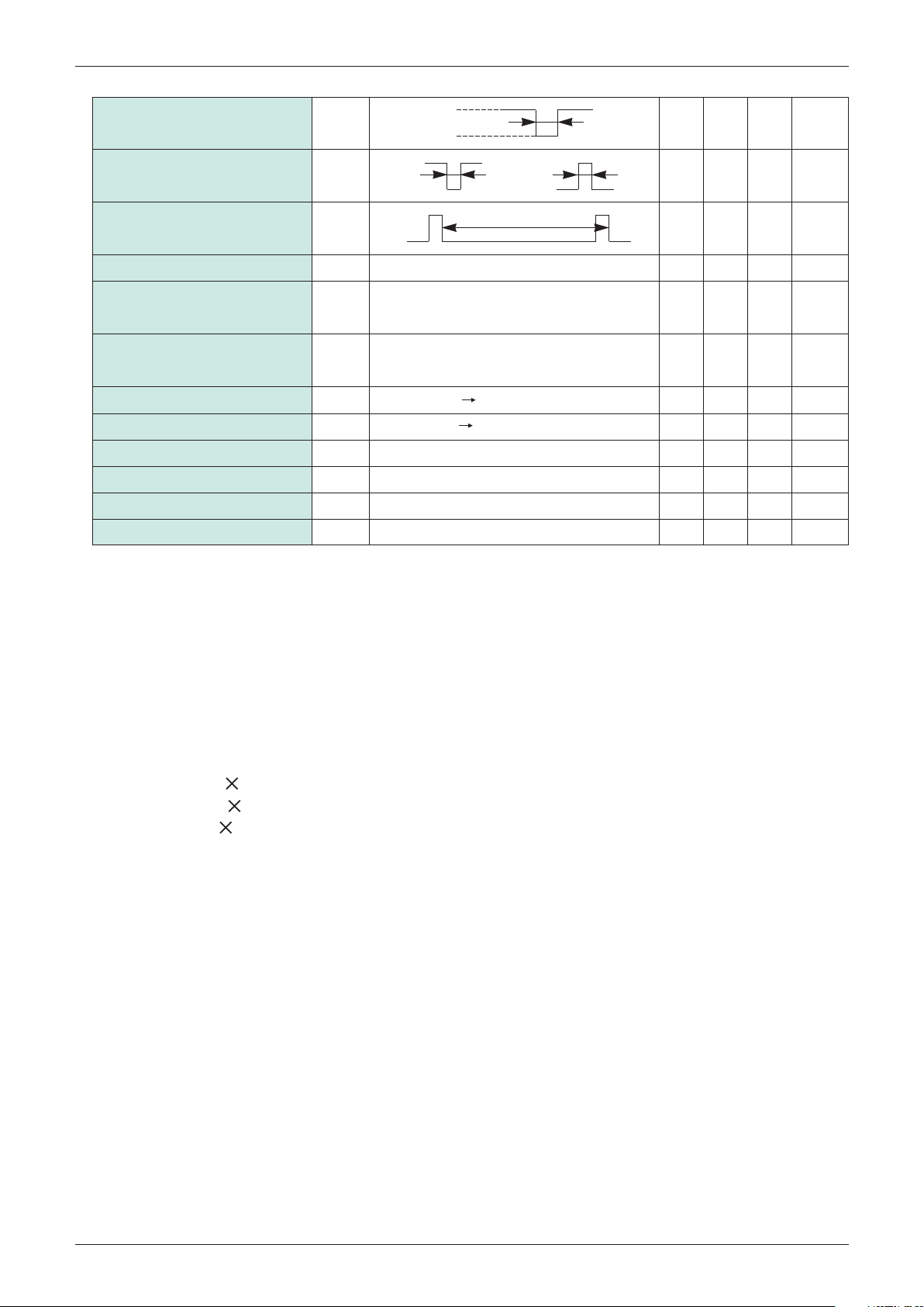
VCC input pulse width 8TPI µS
CK input pulse width T
CKW 3µS
CK input cycle T
CK 20 µS
Watchdog timer monitoring time *1
TWD CT=0.02µF 50 100 150 mS
Watchdog timer
reset time
*
2
T
WR CT=0.02µF 1 2 3 mS
Reset hold time for
power supply rise *3
TPR CT=0.02µF 50 100 150 mS
RESET
------------------------------------------
delay time tPDR
VCC: High Low, R
LR
=10kΩ, C
LR
=15pF
10 µS
BC delay time t
PDB
VCC: High Low, R
LB
=4.7kΩ, C
LB
=15pF
10 µS
RESET
------------------------------------------
rise time tRR RLR=10kΩ, CLR=15pF 10 µS
RESET
------------------------------------------
fall time tFR RLR=10kΩ, CLR=15pF 2 µS
BC rise time t
RB RLB=4.7kΩ, CLB=15pF 10 µS
BC fall time t
FB RLB=4.7kΩ, CLB=15pF 2 µS
VCC
3.8V
2.8V T
PI
CK
T
CKW
or
CK
T
CK
Notes:
*
1 Monitoring time is the time from the last pulse (negative edge) of the timer clear clock pulse until reset
pulse output.
In other words, reset output is output if a clock pulse is not input during this time.
*
2 Reset time means reset pulse width. However, this does not apply to power ON reset.
*
3 Reset hold time is the time from when VCC exceeds detection voltage (VSHR) during power ON reset until
reset release (RESET
-----------------------------------------------------
output high).
*
4 Watchdog timer monitoring time (TWD), watchdog timer reset time (TWR) and reset hold time (TPR) during
power supply rise can be changed by varying C
T capacitance. The times are expressed by the following
formulae.
T
PR (mS)
.
=.5000 CT (µF)
T
WD (mS)
.
=.5000 CT (µF)
T
WR (mS)
.
=.100 CT (µF)
Example : When C
T=0.02µF
T
PR
.
=.100mS
T
WD
.
=.100mS
T
WR
.
=.2mS
*
5TWD can be varied by placing a resistor (1MEGΩ or more) between the RCT pin and VCC.
*
6 The voltage range when measuring output rise and fall time is 10~90%.
*
7VCC rise time should be 100µS or more, and fall time should be 50µS or more.
Page 6

MITSUMI
System Reset (with built-in watchdog timer) MM1135, MM1136
Measuring Circuit
Timing Chart
VCC
CK
C
T
RESET
BC
RCT
TCK
TCKW
TPR
TWR
TWD
VSHB
VSLB
VSMR
VSLR
0.8V
Undefined
Basic Circuit Diagram
 Loading...