

Datasheet MLX32001EE-SO16WTUBE, MLX32001FA-SO16WREEL, MLX32001FA-SO16WTUBE, MLX32001EE-SO16WREEL Datasheet (MELEXIS)
MLX32001
Universal PSTN Line Interface
Page 1 of 11 MLX32001 Universal PSTN Line Interface / Rev1.2 17 May 2000
1. Features and Benefits
§ CLIP / Caller-ID support
§ Line status measuring facilities
§ Line event registration
§ Lightning safe
§ Pre-programming of default settings
§ Powered by PSTN line (less than 10 µA power consumption during offline)
§ SW programmable for worldwide use
2. Applications
§ Analog front-end PSTN interfaces
§ DECT base stations
§ Low / high speed modems
§ Payphones
§ PBX / Fax
§ PC-Voice and mixed voice/data applications
§ Remote configuration / E-pay / POS terminals
§ Settop boxes
§ Utility meter reading
§ VOIP converters on POTS (terminal side)
3. Ordering information
Number Package Description
MLX32001EE-SO16WREEL Plastic small outline package; 16 leads; body width 300 mil
Packed per 1500 pcs REEL
MLX32001EE-SO16WTUBE Plastic small outline package; 16 leads; body width 300 mil
Packed per 22 tubes of 46 pcs / tube = 1012.
MLX32001FA-SO16WREEL Plastic small outline package; 16 leads; body width 300 mil
Packed per 1500 pcs REEL
MLX32001FA-SO16WTUBE Plastic small outline package; 16 leads; body width 300 mil
Packed per 22 tubes of 46 pcs / tube = 1012.
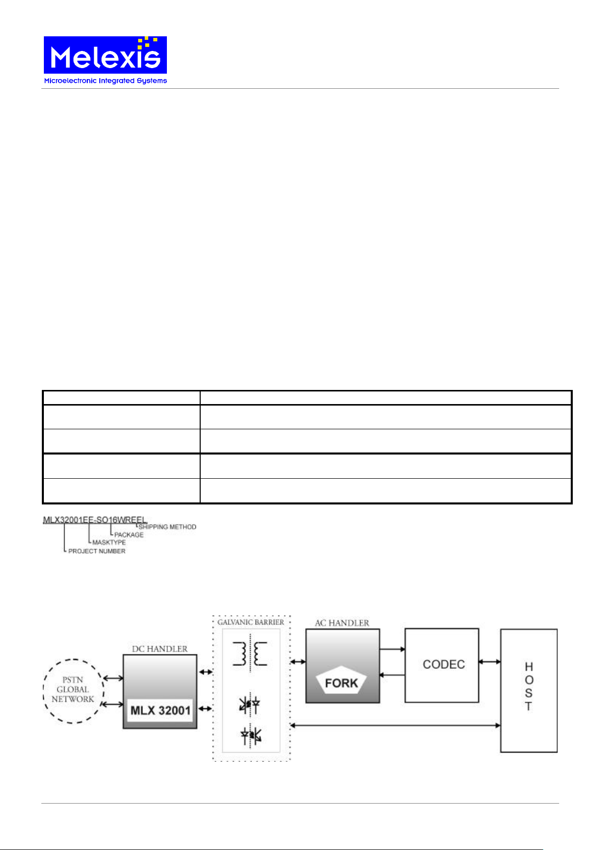
4. Functional Block Diagram
4.1 Modem application
MLX32001
Universal PSTN Line Interface
Page 2 of 11 MLX32001 Universal PSTN Line Interface / Rev1.2 17 May 2000
4.2 PC-Voice application
4.3 PSTN Line powered modem application
5. Description
MLX32001 implements the DC-handler of a universal PSTN
Line Interface. It is fully telephone line powered and digital
control is performed by a special UARTFLEX. There is no
crystal or resonator linked to MLX32001 and thus the core as
well as the UART are capable to adapt themselves to the
HOST UART's preferred communication speeds. The
synchronisation time of the UART is 2400 bps +/- 25%.
To ensure that long term drift and temperature will not affect
communication stability, the communication channel must be
synchronised on a frequent basis. If the line conditions get
low and MLX32001 has to switch down to 1 of its 4 low
power modes, synchronisation locking expires to ensure that
power supply dependent communication times will never
unlock.
There are 64 bytes (512 bits) of user RAM accessible in
MLX32001 to store country and network operator depen-dent
settings. These settings are retrieved from a small parameter
database that supports data originating from the following 3
sources:
1) Type Approval Regulations that more or less specify
the network (e.g. what kind of AC termination is
required; what levels of open line voltages, ring
voltages and online currents can be expected; how are
transient timings for online / offline / CLIP and
polarity dependent phenomena specified, what
common mode unbalance is required)
2) Design and market Experience: Known network errors
and network non-compliance problems can be
implemented in MLX32001 drivers and state machine
to let the line interface properly handle interworking
problems (e.g. how much spikes can be expected
during polarity reversal; how much time does it take
the power supply SLIC to switch between online
detect and online supply mode; what total current
interruptions can be expected; how much time can
pass before an acceptable dialtone is detected)
3) Local Line Adaptation: Local line adaptation is
defined as the ability to measure the telephone line
conditions of the actual network termination point

MLX32001
Universal PSTN Line Interface
Page 3 of 11 MLX32001 Universal PSTN Line Interface / Rev1.2 17 May 2000
where MLX32001 is powered and accordingly adapt
optimally to that telephone network. This means that
MLX32001 is capable of measuring all relevant DC
and transient phenomena on a telephone line that
characterise this line. Consequently settings can be
optimised for (extremely) long line operation, low
current operation, parallel operation with 1 or more
telephones in parallel, line monitoring (detect line
transients, line parallel pickup and replace and total
line disconnect).
In a PC controlled environment, parameters and drivers are
residing in the PC’s memory, while the front end (USB)
controller such as the USB Cypress C7Y67001 is performing
bitwise control and is handling the UART.
MLX32001 is not only a fully line powered device, it also
generates power supply for local hosting microcontrollers. It
has 2 different sources of power supply generation: AUX5,
AUX10 delivering 5 and 10mA nominally if sufficient line
current is available. The AUX5 supply can be programmed in
steps of 20µA. This allows the designer to modify the
HOST's supply current while exactly regulating the supply
voltage with just an internal A/D convertor input on the
HOST.
With those features it is possible to built standalone (modem)
applications with hosting controllers like NEC
UPD78F9177G, Texas Instruments MSP430-series and
Hitachi H8-36XX series. These controllers are then fully line
powered but still perform powerful functions like full V.22
modem implementation, S0 contact scanning for utility
meters, E-data transfer interface for POS and E-cash modules
etc.
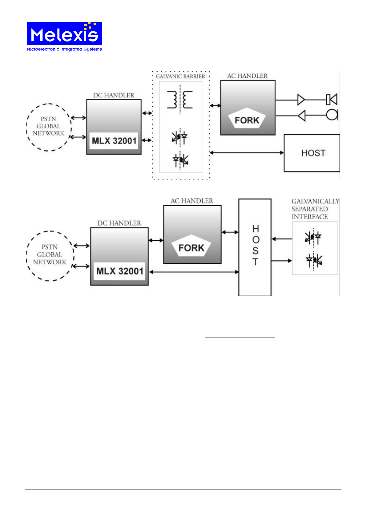
Any line interface requiring galvanic separation has a line
powered PSTN-side and a HOST controller side where
primary controlling power is available. With the MLX32001
there is a consistent and dominant separation between AC
and DC handling:
§ All non-AC handling is regarded as DC handling and is
performed by MLX32001 at the PSTN-powered side,
including (im)pulse dialing, overshoot control, polarity
detection, hookswitch control, ring detection and line
event monitoring. For universal line interface designs,
the DC handling part is always identical
§ All pure AC-handling is performed at the HOST side, as
it differs from application to application and depends on
AC line transformer choice, the number of reference
termination sections and the number of SMTR feedback
filter elements.
For worldwide coverage of Balanced Return Loss 2
impedances are needed. If the design specification is limited
to 600E terminating countries only 1 is required. The
excellent THD and Noise characteristics are the result of the
fully line powered operation. Other DAA's transfer power
supply from the HOST to the PSTN side, giving possible
problems for lightning safety, radio interference at higher
frequencies and frame ground sensitive coupling problems.
The AC-handler part of the design has not been integrated
into MLX32001 for 2 major reasons:
1) In designs that include a galvanic separation, the DC-
handler is on the line powered side, while the AChandler resides on the HOST powered side. Since
MLX32001 supports each possible line transformer,
the DC-handler section is identical for all designs,
while the AC-handler part depends very much on line
transformer selection.
2) For galvanically coupled designs the STMR filters
used require capacitor values up to 2.2µF. Integrating
such high values into silicon will either be expensive
or (with some impedance conversion tricks) will result
in a Total Harmonic Distortion of the transmitting
stage that is higher than the 72dB required by V.90
modems. To allow any design to work with
MLX32001 it was decided to build up any appropriate
AC-handler by conventional components, thus
reaching the best possible THD levels as well as the
most cost effective total design setup.
Interworking reliability is the most important aspect of any
global line interface. MLX32001 design setup has been done
together with a traditional AC-type line transformer for
galvanic barrier implementation. This has the following
advantages:
1) The setup is totally safe for common mode lightning:
there are no high voltage capacitors required between
the PSTN powered side and the HOST powered side.
Since the coupling is inductive, the higher the
frequency, the higher the impedance and the lower the
coupling currents.
2) Proven and reliable electromagnetic coupling
technology
3) 4kV of separation can be reached supporting global
access with 1 transformer
4) 2 standard PC-817 opto-couplers are sufficient to pass
all MLX32001 digital control signals
Finally, MLX32001 supports full line event monitoring. This
means that any line event occurring in online or offline mode
will generate an event within MLX32001 where the host
decides what to do with it. For modems, this means that other
telephones picked up and replaced in parallel can be properly
handled without closing down the connection or terminating
the download procedures. Also MLX32001 can be linked
'virtually' online. In this mode, MLX32001 based designs
never answer incoming calls and never originate calls during
line busy states. Also the actual line use versus daytime
period is 'monitored' and it is consequently decided what is
the best period to make service calls or autodownload
configuration data.
MLX32001
Universal PSTN Line Interface
Page 4 of 11 MLX32001 Universal PSTN Line Interface / Rev1.2 17 May 2000
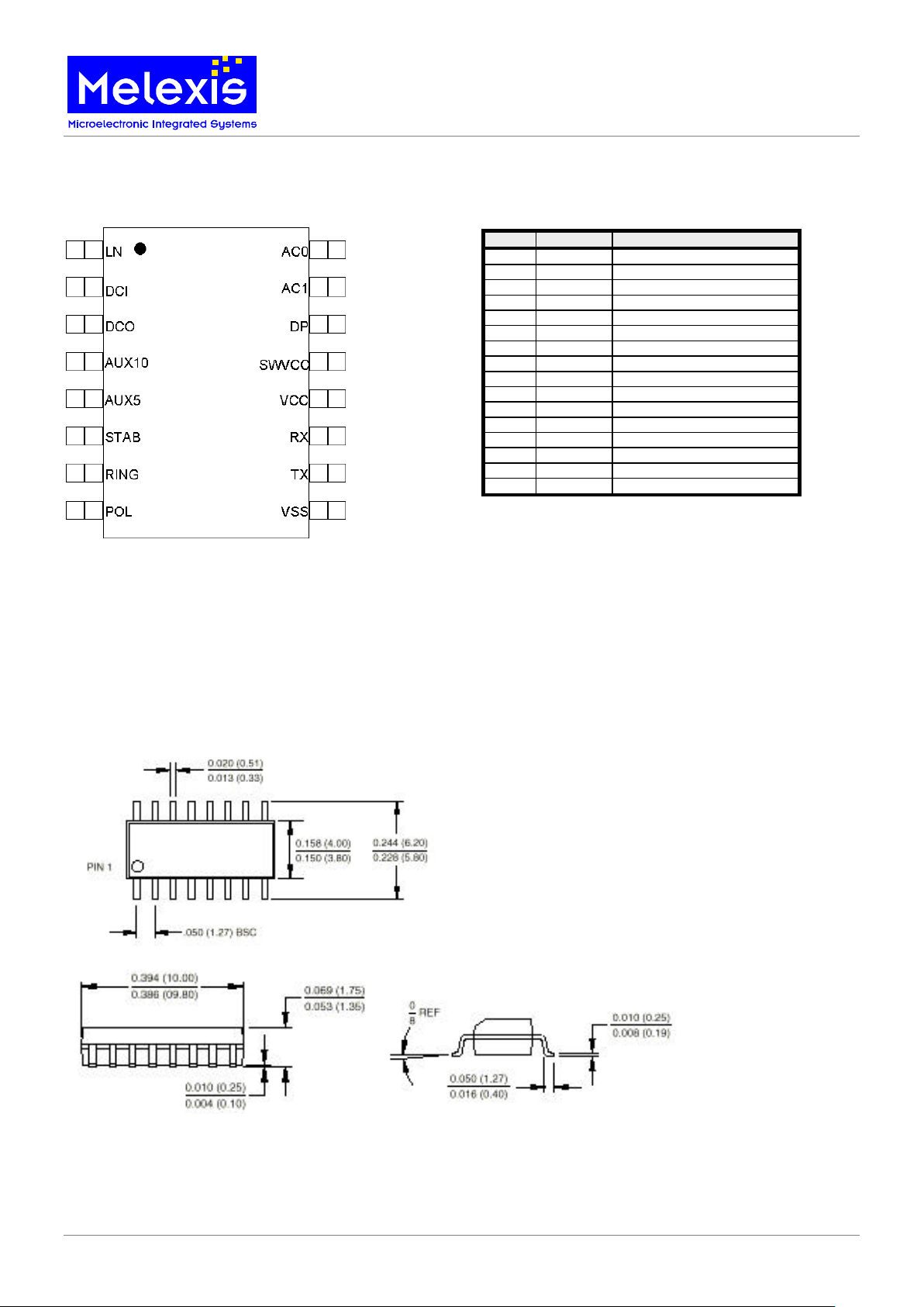
PIN-TYPE DESCRIPTION
PIN NAME PINTYPE
1 LN ANALOG SIGNAL HV
2 DCI ANALOG COIL IN
3 DCO ANALOG COIL OUT
4 AUX10 ANALOG HV
5 AUX5 ANALOG HV
6 STAB ANALOG COIL REFERENCE
7 RING ANALOG INPUT
8 POL ANALOG INPUT
9 VSS GROUND
10 TX DIG OUTPUT
11 RX DIG INPUT
12 VCC POSITIVE POWER SUPPLY
13 SWVCC DIG OUTPUT
14 DP OUTPUT HV
15 AC1 ANALOG SIGNAL HV
16 AC0 ANALOG SIGNAL HV
Note HV = high voltage pin
6. Pin description
PSTN CONNECTED
PINS AT LEFT
HOST CONNECTED
PINS AT RIGHT
Remarks :
• Low voltage signals are on the bottom half. High voltage pins at the upper half.
• RING/POL are grouped together and should be routed together on the pcb.
• LN/DCI are grouped together. The highest possible DC current is flowing through these pins.
• Logic control signals are grouped together (RX, TX).
• AC0/AC1 switches AUX5, AUX10 and DP are as close as possible to LN.
7. Package description, dimensions in inches and (millimeters)

MLX32001
Universal PSTN Line Interface
Page 5 of 11 MLX32001 Universal PSTN Line Interface / Rev1.2 17 May 2000
8. Electrical specifications
Note: All parameters are specified at 20 degrees Celsius and Vcc = 3.3V unless stated otherwise
VCC positive power supply Reference Min Typ Max Unit
Operating supply voltage
V
CC
1.8 3.3 7.2 V
Reduced operating area supply voltage (SOS)
V
CC
1.4 3.2 V
Hysteresis Power-On-Reset circuitry
V
CCHYST
0.6 V
Operating supply currents into LN:
• OFFLINE standby
I
LN
7 15
µµA
• OFFLINE during activity detect
I
LN
70 100
µµA
• OFFLINE during activity detect in SOS
I
LN
140 200
µµA
• ONLINE supply in zener area
I
LN
4.0 4.3 4.6 mA
• ONLINE supply not in zener area
I
LN
3.1 3.3 3.5 mA
LN input
Voltage range
V
LN
-0.6 42 V
ONLINE current
(*) Aux10 and Aux5 active and fully on
I
ONL
0.2 3.3 22.1(*) mA
ONLINE impedance 300-3400Hz DCO off
Z
ONL
40
kΩΩ
Resistor to C
STAB
for DCO control
RLN
STAB
320 400 480
kΩΩ
Resistor to C
STAB
in DCO start mode
RLN
START
15 21 27
kΩΩ
Pin capacitance
C
LN
100 pF
AC signal distortion in 100..10kHz band between either
AC0 and AC1 outputs:
THD -80 dB
LN input (FA Version)
Noise generation in 300…3400 Hz band @ BW = 31Hz
Relative to a 300E termination
P
NOISE
-87 dBm
DCI input
Voltage range
V
DCI
-0.6 VCC+0.6 V
Mute current (V
DCI
=3V)
I
MUTE
-50 mA
Mute offset (VLN - V
DCI
) @ I
MUTE
= 50mA
V
MUTE
1.0 1.5 V
Mute offset (VLN - V
DCI
) @ I
MUTE
= 10mA
V
MUTE
0.3 0.4 V
Input impedance to Ground
R
DCI
70 87 105
kΩΩ
Pin capacitance
C
DCI
50 pF
DCO output
Source current (ß
FEDCO
>= 50, IDC = 100mA)
I
OH
3.5 7.8 mA
Sink current
I
OL
3.0 mA
Q
DCO
DC current gain
Q
DCO HFE
50
Output impedance from DCO
R
DCO
100
ΩΩ
Voltage range
-0.6 3.6 V
Pin capacitance when DCO disabled
C
DCO
50 pF
Output impedance
Z
DCO
100
ΩΩ
AUX10 output
Auxiliary voltage range
V
AUX10
-0.6 42 V
DC Leakage current
I
AUX10LEAK
1
µµA
Supply current
I
AUX10
9.5 10 10.5 mA
Input impedance to Ground when disabled
R
AUX10
10
MΩΩ
Input impedance to LN when enabled
Z
AUX10
1
MΩΩ
Pin capacitance
C
AUX10
20 pF

MLX32001
Universal PSTN Line Interface
Page 6 of 11 MLX32001 Universal PSTN Line Interface / Rev1.2 17 May 2000
AUX5 output
Auxiliary voltage range
V
AUX5
-0.6 42 V
Battery backup current (VLN >= 4V)
I
AUX5BACKUP
-4 -25
µµA
Supply current
I
AUX5
4.5 5 5.5 mA
Input impedance to Ground when disabled
R
AUX5
8
MΩΩ
Input impedance to LN when enabled
Z
AUX5
400
kΩΩ
Pin capacitance
C
AUX5
20 pF
SPYMODE operation:
1 LSB DC current step
IAUX5
STEP
18 20 22
µµA
Spymode Full Range current
I
AUX5
mA
STAB input
Voltage range
V
STAB
-0.6 VCC+0.6 V
Discharge peak current
I
STABDIS
5 mA
DC Leakage @ 1 LSB V
LN
programming error
I
STABLEAK
300 nA
Pin capacitance
C
STAB
3 pF
RING input
Voltage range
V
RING
-0.6 VCC+0.6 V
AC Input impedance relative to C
STAB
ZIN
RING
0.75 1 1.25
MΩΩ
DC Leakage current
I
RINGLEAK
100 nA
Pin capacitance
C
RING
3 pF
POL input
Voltage range
V
POL
-0.6 VCC+0.6 V
AC Input impedance relative to C
STAB
ZIN
POL
0.75 1 1.25
MΩΩ
DC Leakage current
I
POLLEAK
100 nA
Pin capacitance
C
POL
3 pF
TX output
Output voltage LOW (IOL=0.5mA)
VOL
TX
0.3 V
DC Leakage current
I
TXLEAK
100 nA
Output sink current at Vcc > 2.1V
I
TXSINK
1.7 3.5 mA
Max. data transfer cap. in OFFLINE (I
TXSINK
= 500uA)
N
TXMAXBYTES
30 Bytes/s
Pin capacitance
C
TX
3 PF
RX input (FA) version
Quiescent current from RX (VRX = 0V)
RPU
RX
-5
µµA
Input voltage low
VIL
RX
0.1 V
Input voltage high
VIH
RX
0.3 V
Hysteresis
1
V
RXHYST
0 V
Maximum data transfer capacity in OFFLINE
N
RXMAXBYTES
60 Bytes/s
Pin capacitance
C
RX
3 PF
UARTFLEX locking area for 0x55 SYNC_WDR
T
LOCKSPAN
1800 2400 3000 Bits/s
RX input (EE) version
Pull-up resistor to V
CC
RPU
RX
66
kΩΩ
Input voltage low
VIL
RX
0.33Vcc V
Input voltage high
VIH
RX
0.66Vcc V
Hysteresis
V
RXHYST
0.6 V
1
The RX pin in FA version is a current sourced driving pin that eliminates the typical miller capacity problem of an
optocoupler. There is no voltage change on the pin during transfer.

MLX32001
Universal PSTN Line Interface
Page 7 of 11 MLX32001 Universal PSTN Line Interface / Rev1.2 17 May 2000
Maximum data transfer capacity in OFFLINE
N
RXMAXBYTES
30 Bytes/s
Pin capacitance
C
RX
3 pF
UARTFLEX locking area for 0x55 SYNC_WDR
T
LOCKSPAN
1800 2400 3000 Bits/s
SWVCC output
SWVCC Voltage range
V
AUX5
-0.6 VCC+0.6 V
Leakage current (low level)
I
SWVCCLEAK
-1
µµA
Drive current (high level)
I
SWVCC
0.25 0.5 1.0 mA
Pin capacitance
C
SWVCC
6 pF
DP output
DP Voltage range
V
DP
-0.6 42 V
DP Maximum current sink
IOL
DP
200
µµA
DP Leakage current
ILK
DP
100 nA
Capacitance to Ground
C
DPMIN
3.3 nF
Resistance to LN in ONLINE (V
LN
>= 4V)
R
DPLN
10
kΩΩ
AC0 & AC1 output
Voltage range
V
AC
-0.6 42 V
Resistance to LN (closed, V
LN
>= 4V)
RON
AC
16 25 36
ΩΩ
Resistance to GND (1 opened, V
LN
>= 4V)
ROFF
AC
600
kΩΩ
Resistance to GND (both closed, V
LN
>= 4V)
ROFF
AC
350
kΩΩ
Internal clock frequency low speed mode
F
OSCLOW
196 200 204 kHz
Internal clock frequency highspeed mode
F
OSCHIGH
3.136 3.2 3.264 MHz
Operating temperature
T
OPERNORM
0 20 70 °C

MLX32001
Universal PSTN Line Interface
Page 8 of 11 MLX32001 Universal PSTN Line Interface / Rev1.2 17 May 2000
9. Typical application diagrams
9.1 V.90 modem
Block diagram
Line interface, DC-handler and line transformer
DC Handler
A
B
B_HANDSET
A_HANDSET
EURLI STAB
EURLI AC0
EURLI AC1
EURLI GND
EURLI RX
EURLI TX
EURLI VCC
EURLICONTROLBUS
EURLI HV
EURLI LN
EU
RLI
AU
X1
0
EU
RLI
AU
X5
EU
RLI
DP
OFFLINEDATA
Host Application
HOST VCCBUS
HOST GND
EURLI MISO
EURLI MOSI
EURLI RESET
ACTX
ACRX
ACCONTROLBUS
PROG MISO
PROG MOSI
PWRCONTROLBUS
PROGCONTROLBUS
XDSL A
XDSL B
EURLI AUX5
EURLI AUX10
Digital Control
EURLI VCC
EURLI TX
EURLI RX
EURLI GND
HOST VCCBUS
EURLI MOSI
EURLI MISO
HOST GND
EURLI RESET
AC Handler
HOST AC0
HOST GND
HOST VCCBUS
HOST AC1
EURLICONTROLBUS
EURLI HV
EURLI LN
HOST STAB
ACTX
ACRX
ACCONTROLBUS
EURLI VCC
OFFLINEDATA
HOST GND
PSTN Connection
A
B
A_HANDSET
B_HANDSET
XD
SL
A
XD
SL
B
AC Coupling
OFFLINEDATA OFFLINEDATA
EURLI HV
EURLI LN EURLI LN
EURLI HV
EURLI AC0
EURLI AC1
HOST AC0
HOST AC1
EURLI GND HOST GND
EURLI STAB HOST STAB
EURLI VCC EURLI VCC
HOST APPLICATION
HOST AC0
HOST AC1
HOST VCC
HOST GND
EURLI MISO
EURLI MOSI
EURLI RING
EURLI LN
EURLI TX
EURLI DCO EURLI DP
EURLI DCI
EURLI AUX5
EURLI GND
EURLI STAB
EURLI AC0
EURLI AC1
EURLI POL
EURLI SWVCC
HOST VCC
EURLI GND
EURLI VCC
EURLI RX
HOST GND
HOST AC0
HOST AC1
EURLI AC1
EURLI AC0
EURLI HV
OFFLINEDATA
OFFLINEDATA
EURLI AUX10
R2
TNR12G241K
12
F1
FUSE/MJS/1A
1 2
R1
4.7E/Metal Oxide
1 2
L1
TC-250UX2-843
231
4
CON1
PCBHEADER/100E/2P
1
2
1
2
C151
10N/400V
12
T152
BC547B/TO92/600mW
2
1
3
R153
15E
12
T154
BC547B/TO92/600mW
2
1
3
T153
BC547B/TO92/600mW
2
1
3
R152
15E
12
R155
20E/1%/0.5W
12
R154
15E
12
C106
100P/25V
12
C107
100P/25V
12
IC201
PC817A
12
4
3
R201
1K8
12
T201
BC558B
2
3
1
R202
220K
12
R203
10K
12
IC202
PC817A
12
4
3
C303
100N/25V
12
R303
270E
12
C304
100N/25V
12
IC101
EURLI/32001/SOIC16
1
2
3
4
5
6
7
8 9
10
11
12
13
14
15
16
LN(1)
DCI
DCO
AUX10
AUX5
STAB
RING
POL VSS
TX
RX
VCC
SWVCC
DP
AC1
AC0
T151
DN3545N8
1
2 3
R301
220E
12
C301
22U/50V
1 2
TR303
ATS-312
1 3
2 4
D151
1N4004
12
D152
1N4004
12
D153
1N4004
1 2
D154
1N4004
1 2
C103
100U/10V
12
D101
1N4007
1 2
D102
1N4007
1 2
C102
4N7/50V
12
D104
1N4007
12
R102
10M/1%
12
R101
10M/1%
1 2
R105
51K/1%
12
D103
1N4007
12
R104
51K/1%
12
C105
1U/6.3V/MKT/LL
12
C101
4N7/50V
1 2
C104
22N/25V
12
RRINGHIGH
RPOLLOWRRINGLOW
RPOLHIGH
CSTAB
CDP
PSTN
CONNECTION
240V
RSLPE
NOTE: EACH DCO TRANSISTOR MAY
DISSIPATE IN WORST CASE 600mW
TDCO TDCO TDCO
GALVANIC BARRIER
GALVANIC BARRIER

MLX32001
Universal PSTN Line Interface
Page 9 of 11 MLX32001 Universal PSTN Line Interface / Rev1.2 17 May 2000
9.2 PC-Voice
PC-Voice block diagram
PC-Voice line interface and DC-handler
DC Handler
EURLI AC0
EURLI AC1
EURLI GND
EURLI RX
EURLI TX
EURLI VCC
Host Application
HOST VCCBUS
HOST GND
EURLI MISO
EURLI MOSI
ACTX
ACRX
ACCONTROLBUS
Digital Control
EURLI VCC
EURLI TX
EURLI RX
EURLI GND
HOST VCCBUS
EURLI MOSI
EURLI MISO
HOST GND
AC Handler
EURLI AC0
HOST GND
HOST VCCBUS
EURLI AC1
ACTX
ACRX
ACCONTROLBUS
EURLI GND
EURLI RING
EURLI LN
EURLI TX
EURLI DCO EURLI DP
EURLI HV
EURLI DCI
EURLI AUX5
EURLI AUX10
EURLI GND
EURLI STAB
EURLI AC0
EURLI AC1
EURLI RX
EURLI POL
EURLI VCC
EURLI GND
EURLI SWVCC
R1
4.7E/Metal Oxide
1 2
F1
FUSE/MJS/1A
1 2
R2
TNR12G241K
12
CON1
PCBHEADER/100E/2P
1
2
1
2
L1
TC-250UX2-843
2
3
1
4
C151
10N/400V
12
T152
BC547B/TO92/600mW
2
1
3
R152
15E
12
T153
BC547B/TO92/600mW
2
1
3
T154
BC547B/TO92/600mW
2
1
3
R153
15E
12
R154
15E
12
R155
20E/1%/0.5W
12
C107
100P/25V
12
C106
100P/25V
12
IC101
EURLI/32001/SOIC16
1
2
3
4
5
6
7
8 9
10
11
12
13
14
15
16
LN(1)
DCI
DCO
AUX10
AUX5
STAB
RING
POL VSS
TX
RX
VCC
SWVCC
DP
AC1
AC0
T151
DN3545N8
1
2 3
C103
100U/10V
12
D104
1N4007
12
C102
4N7/50V
12
D102
1N4007
1 2
D101
1N4007
1 2
D103
1N4007
12
R105
51K/1%
12
R101
10M/1%
1 2
R102
10M/1%
12
C101
4N7/50V
1 2
C105
1U/6.3V/MKT/LL
12
R104
51K/1%
12
C104
22N/25V
12
EURLI TX
EURLI GND
EURLI VCC
EURLI AC1
EURLI RX
EURLI AC0
RRINGHIGH
RPOLLOW
RRINGLOW
RPOLHIGH
CSTAB
CDP
PSTN
CONNECTION
240V
RSLPE
NOTE: EACH DCO TRANSISTOR MAY
DISSIPATE IN WORST CASE 600mW
TDCO TDCO TDCO

MLX32001
Universal PSTN Line Interface
Page 10 of 11 MLX32001 Universal PSTN Line Interface / Rev1.2 17 May 2000
9.3 Line powered modem / meter reading / POS application
Block diagram
AC- and DC-handler
EURLI RING
EURLI LN
EURLI DCO EURLI DP
EURLI HV
EURLI AUX5
EURLI GND
EURLI STAB
EURLI AC0
EURLI AC1
EURLI POL
EURLI SWVCCEURLI AUX10
EURLI DCI
DVcc
EURLI GND
EURLI RX
EURLI VCC
EURLI TX
EURLI LN
EURLI AUX10
EURLI AUX5
EURLI HV DVcc
R401
4M7
1 2
D401
BAT85
1 2
C401
GOLDCAP 0.047F/5.5V
12
R2
TNR12G241K
12
F1
FUSE/MJS/1A
1 2
R1
4.7E/Metal Oxide
1 2
T152
BC547B/TO92/600mW
2
1
3
C151
10N/400V
12
L1
TC-250UX2-843
231
4
CON1
PCBHEADER/100E/2P
1
2
1
2
R153
15E
12
T154
BC547B/TO92/600mW
2
1
3
T153
BC547B/TO92/600mW
2
1
3
R152
15E
12
R681
270E
12
C107
100P/25V
12
R155
20E/1%/0.5W
12
R154
15E
12
R683
750E12C681
150N/25V
12
R684
330E
12
R682
390E
12
C103
100U/10V
12
T151
DN3545N8
1
2 3
IC101
EURLI/32001/SOIC16
1
2
3
4
5
6
7
8 9
10
11
12
13
14
15
16
LN(1)
DCI
DCO
AUX10
AUX5
STAB
RING
POL VSS
TX
RX
VCC
SWVCC
DP
AC1
AC0
C106
100P/25V
12
C682
56N/25V
12
C683
22U/50V
12
D101
1N4007
1 2
D102
1N4007
1 2
C102
4N7/50V
12
D104
1N4007
12
R102
10M/1%
12
R101
10M/1%
1 2
R105
51K/1%
12
D103
1N4007
12
C104
22N/25V
12
R104
51K/1%
12
C105
1U/6.3V/MKT/LL
12
C101
4N7/50V
1 2
C607
5N6/25V
12
R201
220K
12
R651
10K
12
T201
BC547B
2
1
3
R202
150K
1 2
C651
220N/50V
12
R601
10K
1 2
R605
4K7
12
T602
BC556B
2
3
1
C601
180N/25V
12
R602
220E
12
T601
BC547B
2
1
3
C603
1N/25V
12
C602
470P/25V
12
R604
300E
12
R603
120E
12
R607
75K
1 2
R606
75K
12
EURLI MISO
HOST GND
EURLI MOSI
DVcc
ACTX
STMR FB
ACRX
RRINGHIGH
RPOLLOW
RRINGLOW
RPOLHIGH
CSTAB
CDP
PSTN
CONNECTION
240V
RSLPE
NOTE: EACH DCO TRANSISTOR MAY
DISSIPATE IN WORST CASE 600mW
TDCO TDCO TDCO
DC Handler
A
B
B_HANDSET
A_HANDSET
EURLI STAB
EURLI AC0
EURLI AC1
EURLI GND
EURLI RX
EURLI TX
EURLI VCC
EURLICONTROLBUS
EURLI HV
EURLI LN
EURLI AUX10
EURLI AUX5
EURLI DP
OFFLINEDATA
Host Application
HOST VCCBUS
HOST GND
EURLI MISO
EURLI MOSI
EURLI RESET
ACTX
ACRX
ACCONTROLBUS
PROG MISO
PROG MOSI
PWRCONTROLBUS
PROGCONTROLBUS
XDSL A
XDSL B
EURLI AUX5
EURLI AUX10
Digital Control
EURLI VCC
EURLI TX
EURLI RX
EURLI GND
HOST VCCBUS
EURLI MOSI
EURLI MISO
HOST GND
EURLI RESET
Power Supply
EURLI VCC
EURLI HV
EURLI LN
EURLI AC0
EURLI AC1
A
B
EURLI GND
EURLI DP
EURLI AUX5
EURLI AUX10
HOST GND
PWRCONTROLBUS
HOST VCCBUS
AC Handler
HOST AC0
HOST GND
HOST VCCBUS
HOST AC1
EURLICONTROLBUS
EURLI HV
EURLI LN
HOST STAB
ACTX
ACRX
ACCONTROLBUS
EURLI VCC
OFFLINEDATA
HOST GND
PSTN Connection
A
B
A_HANDSET
B_HANDSET
XDSL A
XDSL B
AC Coupling
OFFLINEDATA OFFLINEDATA
EURLI HV
EURLI LN EURLI LN
EURLI HV
EURLI AC0
EURLI AC1
HOST AC0
HOST AC1
EURLI GND HOST GND
EURLI STAB HOST STAB
EURLI VCC EURLI VCC

MLX32001
Universal PSTN Line Interface
Page 11 of 11 MLX32001 Universal PSTN Line Interface / Rev1.2 17 May 2000
Host application and RX-amplifier
10. Information
For ordering please contact:
Melexis Swiss Branch
38, Chemin de Buchaux
CH-2022 Bevaix
Switzerland
Phone +41 (4132)8470660
Fax +41 (4132)8470699
E-mail: iva@melexis.com
Web: www.melexis.com
For design information please contact:
Joritel International B.V.
Mr Rien van der Linden
Fregatstraat 99
3534 RC Utrecht
Netherlands
Phone: +31 (30)2421519
Fax: +31 (30)2442176
E-mail: rien@joritel.nl
Web: www.joritel.nl
IICC
IICD
PGM_FVpp
TXD
HOST GND
HOST GND
RXD
PGM_/RES
EURLI MOSI
DAC3
TXD
DAC5
EEGND
EEGND
DAC0
LEDR
PGM_FVpp
PGM_/RES
EURLI MISO
IICD
DAC4
RXGAIN1
DAC2
AVCC/2
IICC
/SWAVCC
DAC1
RXD
STMR FB
FSK_in
/SWAVCC
AVref
AVref
LEDR
DVcc
DVccDVcc
EURLI MISO
EURLI MOSI
STMR FB
AVCC
DVcc
DVcc
DVcc
HOST GND
HOST GND
HOST GND
HOST GND
AVCC/2
HOST GND
AVCC
HOST GND
RXGAIN0
DVcc
T802
BC556B
2
3
1
LED801
LED3MM/RED/2mA
2 1
R842
1K
12
C807
100N/25V
12
R810
10K
12
LED802
LED3MM/GRN/2mA
2 1
R841
1K
12
C815
22N/25V
1 2
R848
100K
12
R847
100K
12
C804
22P/25V
12
R809
1K
1 2
C806
15P/25V
12
X801
5MHz
1 2
C803
22P/25V
12
C805
15P/25V
12
X802
32KHz
1 2
T811
BC547B
2
1
3
R827
220K
12
T813
BC558B
2
3
1
R832
1K
12
R831
47K
1 2
R829
220K
12
R828
3K3
12
R830
1K5
12
T812
BC547B
2
1
3
R835
1K8
12
C812
47P/25V
1 2
C813
470P/25V
1 2
C811
22N/25V
12
R837
820E
1 2
R839
1K
12
C814
22N/25V
1 2
NEC
QFP44
IC801
NEC/PD78F9177_QFP44
1
2
3
4
5
6
7
8
9
10
11
12
13
14
15
16
17
18
19
20
21
22
44
43
42
41
40
39
38
37
36
35
34
33
23
24
25
26
27
28
29
30
31
32
P60/ANI0
P61/ANI1
P62/ANI2
P63/ANI3
P64/ANI4
P65/ANI5
P66/ANI6
P67/ANI7
AVss
P10
P11
P30/INTP0TI81/CPT90
P31/INTP1/TO81
P32/INTP2/TO90
P33/INTP3/TO82/BZO90
P20/SCK20/ASCK20
VDD1
P21/SO20/TxD20
P22/SI20/RxD20
P23
P24
Vpp
AVref
AVdd
P53
P52
P51
P50
P05
VSS1
P04
P03
P02
P01
XT2
XT1
RESET
X2
X1
VSS0
VDD0
P25/TI80/SS20
P26/TO80
P00
R840
1K
1 2
R808
10K
12
R818
10K/1%
12
R811
20K/1%
12
R821
10K/1%
12
R822
10K/1%
12
R819
10K/1%
12
R820
10K/1%
12
R814
20K/1%
12
R812
20K/1%
12
R813
20K/1%
12
R815
20K/1%
12
R816
20K/1%
12
C809
22N/25V
12
IC802
24C02A/P
1
2
3
4
8
7
6
5
A0
A1
A2
GND
VCC
WP
SCL
SDA
C801
22N/25V
1 2
CON803
PINROW/10PD
1 2
3 4
5 6
7 8
9 10
1 2
3 4
5 6
7 8
9 10
R854
22K
12
R824
20K/1%
12
R852
22K
12
R853
22K
12
C810
100N/25V
12
ACTX
DVcc
STMR FB
EURLI MISO
EURLI MOSI
ACRX
PROGRAMMER
OPTION
RXGAIN1 is low => +8dB gain
otherwise RXGAIN1 = HIGH-Z
RXGAIN0 is low => +16dB gain
otherwise RXGAIN0 = HIGH-Z
 Loading...