

Page 1
MLX10410
8 Fold High Side Driver
Features and Benefits
Small package (SOIC20)
Short-circuit protection
Diagnostic features
Current limitation
Low-power consumption
Over-temperature protection
Direct micro controller compatible
Integrated free wheel diodes
Applications
Automotive climate Control
Dashboard
Industrial Actuator control
Ordering Information
Part No. Temperature Suffix Package Temperature Range
MLX10410CA N/A SOIC-20 -40C to 85C Automotive
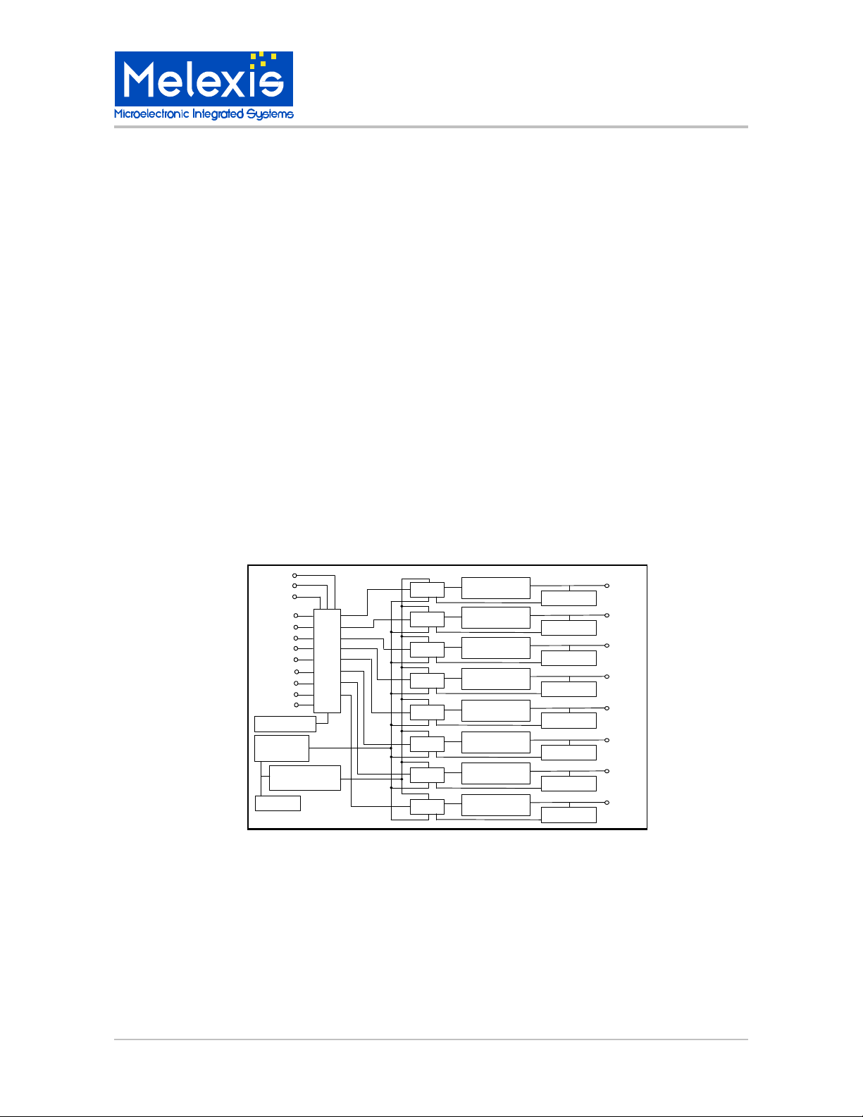
Functional Diagram
VDD
VCC1
VCC2
ADR2
ADR1
ADR0
CEN
STROBE
DATAI
DATAO
OTB
GND
OSCILLATOR
OVER-TEMP
PROTECT
BG OVER-VOLT
PROTECT
STAND-BY
LOGIC
LOGIC
LOGIC
LOGIC
LOGIC
LOGIC
LOGIC
LOGIC
OUTPUT
CURRENT LIMIT
OUTPUT
CURRENT LIMIT
OUTPUT
CURRENT LIMIT
OUTPUT
CURRENT LIMIT
OUTPUT
CURRENT LIMIT
OUTPUT
CURRENT LIMIT
OUTPUT
CURRENT LIMIT
OUTPUT
CURRENT LIMIT
Figure 1
DETECT C.C.
OUT7
OUT6
DETECT C.C.
OUT5
DETECT C.C.
OUT4
DETECT C.C.
OUT3
DETECT C.C.
OUT2
DETECT C.C.
OUT1
DETECT C.C.
OUT0
DETECT C.C.
Description
The 10410 is a high-side driver for automotive applications. It can drive small lamps, relays, coils etc. The output current
can be up to 250mA per driver (current limit at minimum 250mA).
The IC will only react to commands on the bus if the CEN (chip enable) signal is high. The CEN signal has nothing to do
with the power down mode, the IC will react to the micro controller commands if CEN is high.
MLX902xx Name of Sensor Rev Y.X 22/Aug/98 Page 1
MLX10410 8 Fold High Side Driver Page 1 Rev 1.1 16/Apr/01
Page 2
MLX10410
8 Fold High Side Driver
In order to switch a particular output, it is necessary to apply its address on the 3 bit bus and the data on the input
DATAI. A high level on STROBE will latch the data and switch the output. When the IC is in active mode and CEN is
high, the logic level of the addressed output will be available on the pin DATAO.
When all 8 outputs are inactive (latched value is low) the circuit automatically switches to power down mode.
Diagnostic mode: when the DATAI is low and the STROBE is high, a 50K pull up to VCC is switched on, on the
corresponding output channel (addressed by ADR2, ADR1, ADR0) to see whether there is a load connected. The logic
level of the output can be observed on the pin DATAO. In this way, it is possible to scan all the outputs for an open
circuit.
When the IC is in active mode, then there is an over-temperature sensor that monitors the temperature of the IC. If the
die temperature goes above 165°C, all outputs are switched off and the output OTB will go low. As soon as the
temperature decreases below 125°C all outputs are switched back to their previous state.
The outputs are short-circuit proof against GND and VCC. When an output is shorted to GND, the current is limited and,
after a delay of typically 20ms, the output is switched off and the output OTB goes low. A delay is used to guarantee that
the output does not detect a short circuit when a normal lamp is driven. The latched value of the ouput is set to 0. A
rising edge on CEN will set OTB back to 1. When an output is shorted to a supply larger than VCC+100mV, the output
driver bulk is immediately disconnect from VCC, and after a delay of typically 20ms, the output is switched off and the
output OTB goes low. The latched value of the ouput is set to 0. A rising edge on CEN will set OTB back to 1
There is an over-voltage shut off that switches all the outputs off when the VCC voltage is above 18V for at least 1ms.
When an over-voltage occurs, CEN being low, DATAO pin will go low. The outputs will come on again as soon as the
voltage decreases below 18V. The status of all 8 outputs stays latched.
Every output stage is protected with a free wheel diode both to ground and to VCC.
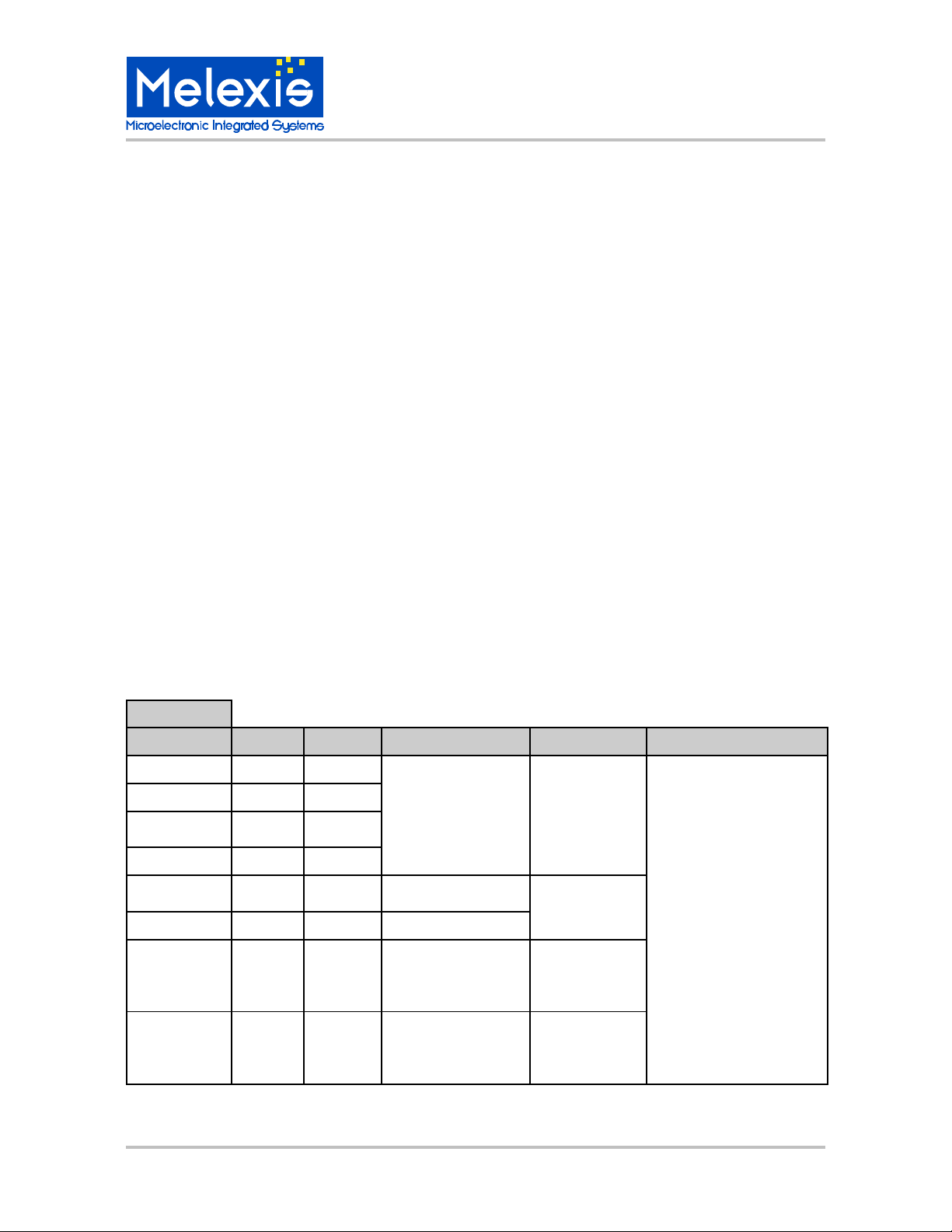
Table 1
Active mode
CEN STROBE DATA I Description
0 0 0
0 0 1
0 1 0
0 1 1
1 0 0 No Command Addressed
1 0 1 No Command
1 1 0 Addressed output 0 Load
turned OFF
1 1 1 Addressed output
DATA O
Chip 0 Over-voltage
Disabled 1 No Over-
voltage
OR
output
logic level
1 No Load
(Diagnostic mode)
Addressed
turned ON
output logic
level (always
1)
0 Over-temperature
Short-circuit to
1 No Over-
OTB
GND
temperature
MLX10410 8 Fold High Side Driver Page 2 Rev 1.1 16/Apr/01
Page 3

ABSOLUTE MAXIMUM RATINGS
VCC -0.3 to 40V
VDD -0.3 to 5.5V
Maximum Output Voltage -0.3V to VCC+0.3V
MLX10410
8 Fold High Side Driver
Maximum Output Current
Maximum Free-Wheel Diodes Current
Die Temperature +170°C
Thermal Resistance Package
Storage Temperature -55 °C to 125°C
ESD Protection all pins
(human body model)
DYNAMIC CHARACTERISTICS
Characteristics
t
sw
t
sds
t
hds
t
scs
STROBE pulse width 1.0 us
DATAI to STROBE setup time 0.1 us
DATAI to STROBE hold time 0.1 us
CEN to STROBE setup time 0.1 us
Description
±550mA
±250mA
85°K/W
2KV
Limits
Min Typ Max Units
t
shs
t
dso
t
dov
t
dso
t
rov
MLX902xx Name of Sensor Rev Y.X 22/Aug/98 Page 3
MLX10410 8 Fold High Side Driver Page 3 Rev 1.1 16/Apr/01
STROBE to OUTPUT delay (Ron reached 20%
Delay between Over voltage detection and out-
Delay between short circuit detection and out-
Recovery time from an over voltage detection 10 us
CEN to STROBE hold time 0.1 us
10 us
of nominal value)
0.5 1.0 2.0 ms
puts switched off
12 20 40 ms
put switched off
Page 4

MLX10410
8 Fold High Side Driver
Electrical Characteristics
Following characteristics are valid over the temperature range from –40°C to +85°C
unless otherwise specified.
Characteristics
Supply voltage VDD
Supply voltage VCC
Supply current Iccs
Supply current Icca
Supply current Icci
Supply current Iccm
Supply current Idds
Supply current Idda
Supply current Iddi
Test Conditions
all outputs switched off
all outputs on and no load
VCC=12V, one output on
and no load
VCC=12V, one output on,
no load, per supplemen-
tary output on
all outputs switched off
all outputs on and no load
one output on and no load
Limits
Min Typ Max
4.5 5.0 5.5 V
4.5
1000
25
Units
25 V
200 µA
µA
200 µA
µA
100 µA
500 µA
150 µA
Input threshold
ADR2, ADR1, ADR0, DATAI,
STROBE, CEN
Input hysteresis
ADR2, ADR1, ADR0, DATAI,
STROBE, CEN
Input current
ADR2, ADR1, ADR0, DATAI,
STROBE, CEN
Vol
DATAO, OTB
Voh
DATAO
Iohl
OTB
Input threshold
OUT7-0
Pull up resistor
Output resistance
Ron(OUT7-0)
Output current limitation
Ilim(OUT7-0)
Output short circuit threshold
(OUT7-0)
Over voltage Shut-Off threshold
Over voltage Shut-Off Hysteresis
VDD=5V and
0<Vin<VDD
Iout=1mA
Iout=1mA VDD-0.5
Vout=5V -1.0
diagnostic mode 0.2*VDD
diagnostic mode 25 50 100
active mode
Iout=200mA, VCC=12V
VCC=12V and Vout=0V 250
VCC 18.0 21.0 24 V
VCC
0.25*VDD
-1.0 0.0 1.0 µA
2/3VCC -0.5 2/3VCC 2/3VCC +0.5 V
0.1*VDD
2.5 4.0
1.0
0.75*VDD V
0.5 V
1.0 µA
0.3*VDD V
500 mA
V
V
KΩ
Ω
V
Over temperature Shut-Off
MLX10410 8 Fold High Side Driver Page 4 Rev 1.1 16/Apr/01
Tj 150 165 180
°C
Page 5

MLX10410
8 Fold High Side Driver
Name
Function
VCC1, VCC2 power inputs, both inputs need to be connected.
GND circuit ground
VDD 5V logic supply
OUT7, OUT0 power outputs
DATAI data input
STROBE data is latched on the high level of strobe
ADR2, ADR1, ADR0 address for output selection
DATAO data output
OTB open drain output that indicates that the IC is in over tempera-
ture protection
CEN chip enable signal (in a system with only one IC, it is possible
to connect this signal directly to VDD).
Pin Assignment
Pin 1: VDD Pin 20: CEN
Pin 2: OTB Pin 19: DATAO
Pin 3: GND Pin 18: OUT7
Pin 4: OUT0 Pin 17: OUT6
Pin 5: OUT1 Pin 16: VCC
Pin 6: VCC Pin 15: OUT5
Pin 7: OUT2 Pin 14: OUT4
Pin 8: OUT3 Pin 13:STROBE
Pin 9:ADR2 Pin 12:DATAI
Pin 10:ADR1 Pin 11: ADR0
For the latest version of this document,
Go to our website at:
www.melexis.com
Or for additional information
contact Melexis Direct:
USA
Melexis Inc.
41 Locke Road, Concord, NH 03301
Phone: +1 603 223 2362 Fax: +1 603 223 9614
E-mail: sales_usa@melexis.com
United Kingdom
Silicon Concepts
PCB Lynchborough Road, Hampshire GU30 7SB, United Kingdom
Phone: +44 1428 751 617 Fax: +44 1428 751 603
E-mail: sales_uk@melexis.com
Germany
Am Seestern 8, 40547 Düsseldorf, Germany
Phone: +49 211 5360212 Fax: +49 211 5360250
E-mail: sales_de@melexis.com
France
Melexis France
Tour Arago, 5 rue Bellini, 92806 Puteaux-La-Défense, France.
Phone: +33 1 47 78 11 34 Fax: +33 1 47 78 06 35
E-mail: sales_france@melexis.com
Italy
Dimacred IRL
Via Papa Giovanni XXIII no. 25, 20046 Biassono, Italy
Phone: +39 039 249 4856 Fax: +39 039 491773
E-mail: sales_italy@melexis.com
Japan
Satori Electric Co., LTD
1-14-10 Shiba, Minato-Ku, Tokyo, Japan
Phone: +81 3 3452 7171 Fax: +81 3 3769 2197
E-mail: sales_japan@melexis.com
Taiwan
Beechwood Int’l Taiwan Co.
Room 8, 17F, No. 189, Taipei, Taiwan
Phone: +886 2 2739 3322 Fax: +886 2 2739 3090
E-mail: sales_taiwan@melexis.com
MLX902xx Name of Sensor Rev Y.X 22/Aug/98 Page 5
MLX10410 8 Fold High Side Driver Page 5 Rev 1.1 16/Apr/01
 Loading...