

Page 1
MLO 75
MMO 75
AC Controller Modules
V
RSMVRRM
V
DSMVDRM
Type
MLO
G1 K1
VV
1200 1200 MLO 75-12io1 MMO 75-12io1
1600 1600 MLO 75-16io1 MMO 75-16io1
K2
Symbol Test Conditions Maximum Ratings
I
RMS
I
TRMS
I
TAVM
I
TSM
TK = 85°C, 50 - 400 Hz (for single controller) 86 A
TVJ = T
VJM
TK = 85°C; (180° sine) 39 A
TVJ = 45°C; t = 10 ms (50 Hz), sine 1150 A
VR = 0 t = 8.3 ms (60 Hz), sine 1230 A
TVJ = T
VJM
VR = 0 t = 8.3 ms (60 Hz), sine 1100 A
t = 10 ms (50 Hz), sine 1000 A
I2t TVJ = 45°C t = 10 ms (50 Hz), sine 6600 A2s
VR = 0 t = 8.3 ms (60 Hz), sine 6280 A2s
(di/dt)
(dv/dt)
P
GM
P
GAVM
V
RGM
T
VJ
T
VJM
T
stg
V
ISOL
M
d
TVJ = T
VJM
VR = 0 t = 8.3 ms (60 Hz), sine 5020 A2s
cr
TVJ = T
VJM
f =50 Hz, tP =200 ms
VD = 2/3 V
IG = 0.45 A non repetitive, IT = I
DRM
diG/dt = 0.45 A/ms
TVJ = T
cr
RGK = ¥; method 1 (linear voltage rise)
TVJ = T
= I
I
T
;V
VJM
VJM
TAVM
50/60 Hz, RMS t = 1 min 3000 V~
£ 1 mA t = 1 s 3600 V~
I
ISOL
Mounting torque (M3) 0.7 ± 0.1 Nm
t = 10 ms (50 Hz), sine 5000 A2s
repetitive, IT = 150 A 100 A/ms
TAVM
= 2/3 V
DR
DRM
1000 V/ms
tp = 30 ms10W
tp = 300 ms5W
-40...+125 °C
-40...+125 °C
(UNF 4-32) 6 ± 0.9 lb.in.
Weight typ. 15 g
MMO
G1 K1
K2 G2
62 A
500 A/ms
0.5 W
10 V
125 °C
I
RMS
V
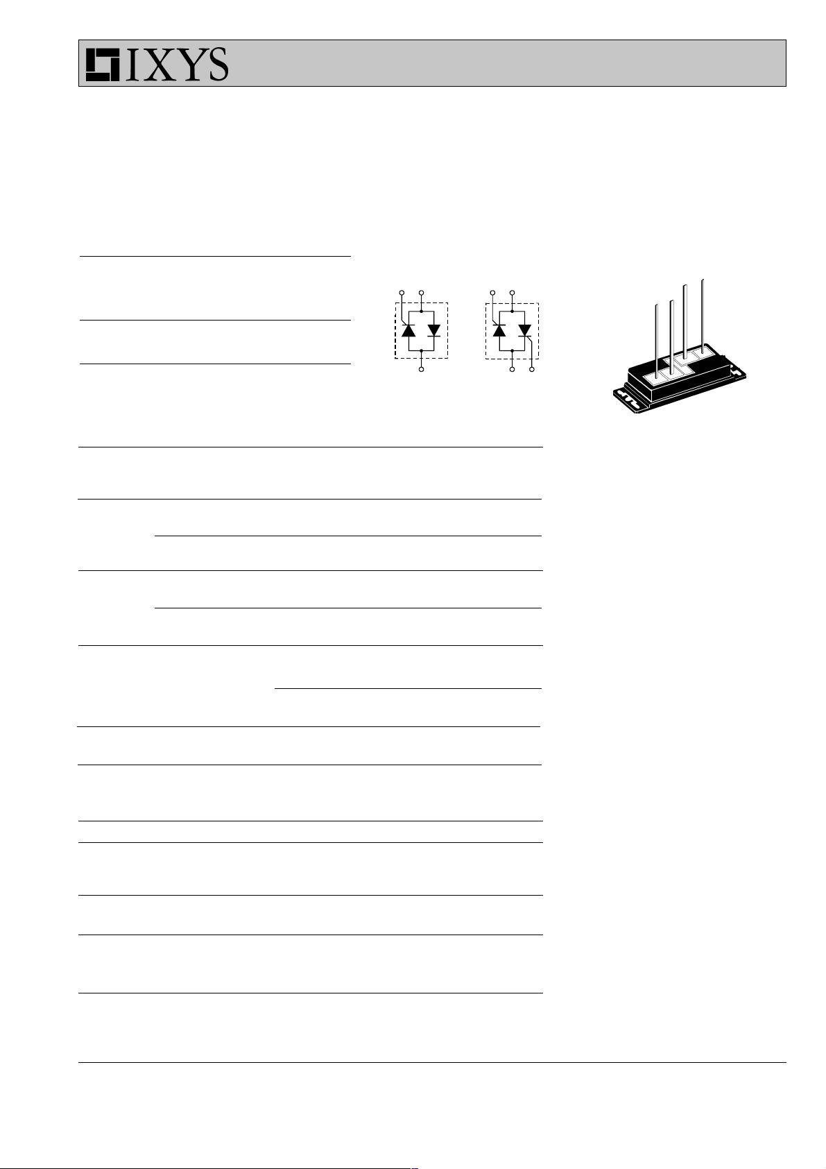
MMO 75
= 86 A
= 1200-1600 V
RRM
K1
G2
K2
G1
K1 = Cathode 1, G1 = Gate 1
K2 = Cathode 2, G2 = Gate 2
(MLO 36 has no G2 lead)
Features
●
Thyristor controller for AC (circuit
W1C acc. to IEC) for mains frequency
●
Direct copper bonded Al2O3 -ceramic
base plate
●
Isolation voltage 3600 V~
●
Planar passivated chips
●
UL registered, E 72873
●
Long wire leads suitable for PC board
soldering
Applications
●
Switching and control of single and
three phase AC
●
Softstart AC motor controller
●
Solid state switches
●
Light and temperature control
Advantages
●
Easy to mount with two screws
●
Space and weight savings
●
Improved temperature and power
cycling
●
High power density
Data according to IEC 60747 and to a single thyristor/diode unless otherwise stated.
IXYS reserves the right to change limits, test conditions and dimensions.
© 2000 IXYS All rights reserved
1 - 3
Page 2
MLO 75
MMO 75
Symbol Test Conditions Characteristic Values
, I
I
R
D
V
T
V
T0
r
T
V
GT
I
GT
I
GM
V
GD
I
GD
I
L
I
H
t
gd
t
q
R
thJC
R
thJK
d
S
d
A
a Max. allowable acceleration 50 m/s
TVJ= T
; VR = V
VJM
RRM
; VD = V
DRM
£ 5mA
IT= 100 A; TVJ = 25°C £ 1.4 V
For power-loss calculations only 0.85 V
5.0 mW
VD = 6 V; TVJ = 25°C £ 1.5 V
TVJ = -40°C £ 1.6 V
VD = 6 V; TVJ = 25°C £ 150 mA
TVJ = -40°C £ 200 mA
tp = 50 ms, f = 60 Hz, IT = I
TVJ = T
;V
VJM
D
= 2/3 V
TAVM
DRM
£ 0.25 V
£ 5mA
6A
TVJ = 25°C; tP = 10 ms, VD = 6 V £ 300 mA
IG = 0.45 A; diG/dt = 0.45 A/ms
TVJ = 25°C; VD = 6 V; RGK = ¥ £ 100 mA
TVJ = 25°C; VD = 1/2 V
IG = 0.45 A; diG/dt = 0.45 A/ms
TVJ = T
VR = 100 V; dv/dt = 15 V/ms; VD = 2/3 V
; IT = 50 A, tP = 200 ms; -di/dt = 10 A/ms typ. 150 ms
VJM
DRM
DRM
£ 2 ms
per thyristor/diode; DC current 0.55 K/W
per module 0.275 K/W
per thyristor/diode; DC current 0.75 K/W
per module 0.375 K/W
Creeping distance on surface 4.5 mm
Creepage distance in air 4.5 mm
10
1: I
, T
= 125°C
GT
VJ
, T
= 25°C
2: I
GT
3: I
VJ
, T
= -40°C
GT
VJ
V
V
G
1
1
I
, T
= 125°C
GD
0.1
VJ
1 10 100 1000
Fig. 1 Gate trigger characteristics
1000
µs
t
gd
100
2
10
typ.
2
Limit
3
4
4: P
5: P
6: P
GAV
GM
GM
5
= 0.5 W
= 5 W
= 10 W
6
mA
I
G
T
= 25°C
VJ
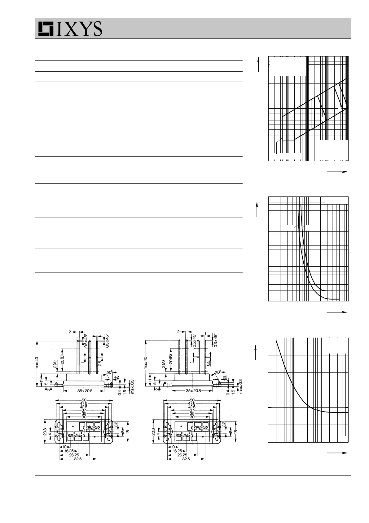
Dimensions in mm (1 mm = 0.0394")
MLO 75 MMO 75
1
10 100 1000
mA
I
G
Fig. 2 Gate trigger delay time
300
A
250
I
RMS
200
150
100
50
0
0.01 0.1 1 10
T
VJ
T
K
t
= 125°C
= 85°C
s
MMO 75
MLO 75
Fig. 3 Rated RMS current versus time
(360° conduction)
© 2000 IXYS All rights reserved
2 - 3
Page 3

MLO 75
MMO 75
110
W
100
90
P
tot
80
70
60
50
K/W
R
thKA
0.3
0.9
1.2
1.5
3
6
40
30
20
10
0
0 20406080
Circuit W1
1 x MMO 75
1 x MLO 75
I
RMS
0 25 50 75 100 125 150
A
T
A
°C
Fig. 4 Load current capability for single phase AC controller
330
W
300
270
P
tot
240
210
180
150
R
0.1
0.3
0.4
0.5
1
2
thKA
K/W
120
90
60
30
0
0 20406080
Circuit W3
3 x MMO 75
3 x MLO 75
I
RMS
0 25 50 75 100 125 150
A
TA
°C
Fig. 6 Load current capability for three phase AC controller: 3xMMO 75/MLO 75
1000
A
50 Hz
80 % V
RRM
800
I
TSM
600
= 45°C
T
VJ
400
T
= 125°C
VJ
200
0
1 10 100 1000
ms
t
Fig. 5 Surge overload current
I
, I
: Crest value, t: duration
TSM
FSM
10000
I
VR = 0V
2
A
s
T
= 45°C
VJ
2
t
T
= 125°C
VJ
300
200
1000
110
ms
t
Fig. 7 I2t versus time (1-10 ms)
1.0
Constants for
K/W
Z
calculation:
thJK
/ (K/W) ti / (s)
R
0.8
Z
thJK
thi
0.019 0.004
0.034 0.02
0.498 0.16
0.6
0.2 0.68
0.4
0.2
0.0
0.001 0.01 0.1 1 10 100
R
for various
thJK
conduction
angles d:
R
/ (K/W) d :
thJK
0.751 DC
0.792 180°
0.813 120°
0.841 60°
0.86 30°
t
Fig. 8 Transient thermal impedance junction to heatsink
(per thyristor or diode)
© 2000 IXYS All rights reserved
30°
60°
120°
180°
DC
s
70
A
60
I
TAVM
50
40
30
20
10
0
0 25 50 75 100 125
Fig. 9 Maximum on-state current
T
K
versus heatsink temperature
DC
180° sin
120°
60°
30°
°C
3 - 3
 Loading...