

Page 1
1
Motorola TMOS Power MOSFET Transistor Device Data
SMARTDISCRETES
Internally Clamped, Current Limited
N–Channel Logic Level Power MOSFET
The MLD2N06CL is designed for applications that require a rugged power switching
device with short circuit protection that can be directly interfaced to a microcontrol unit
(MCU). Ideal applications include automotive fuel injector driver, incandescent lamp
driver or other applications where a high in–rush current or a shorted load condition could
occur.
This logic level power MOSFET features current limiting for short circuit protection,
integrated Gate–Source clamping for ESD protection and integral Gate–Drain clamping
for over–voltage protection and Sensefet technology for low on–resistance. No additional
gate series resistance is required when interfacing to the output of a MCU, but a 40 kΩ
gate pulldown resistor is recommended to avoid a floating gate condition.
The internal Gate–Source and Gate–Drain clamps allow the device to be applied
without use of external transient suppression components. The Gate–Source clamp
protects the MOSFET input from e lectrostatic v oltage s tress up t o 2.0 kV. The
Gate–Drain clamp protects the MOSFET drain from the avalanche stress that occurs
with inductive loads. Their unique design provides voltage clamping that is essentially
independent of operating temperature.
The MLD2N06CL is fabricated using Motorola’s SMARTDISCRETES technology which
combines the advantages of a power MOSFET output device with the on–chip protective
circuitry that can be obtained from a standard MOSFET process. This approach offers an
economical means of providing protection to power MOSFETs from harsh automotive and
industrial environments. SMARTDISCRETES devices are specified over a wide temperature range from –50°C to 150°C.
MAXIMUM RATINGS
(TJ = 25°C unless otherwise noted)
Rating
Symbol Value Unit
Drain–to–Source Voltage V
DSS
Clamped Vdc
Drain–to–Gate Voltage (RGS = 1.0 MΩ) V
DGR
Clamped Vdc
Gate–to–Source Voltage — Continuous V
GS
±10 Vdc
Drain Current — Continuous @ TC = 25°C I
D
Self–limited Adc
Total Power Dissipation @ TC = 25°C P
D
40 Watts
Electrostatic Voltage ESD 2.0 kV
Operating and Storage Temperature Range TJ, T
stg
–50 to 150 °C
THERMAL CHARACTERISTICS
Maximum Junction Temperature T
J(max)
150 °C
Thermal Resistance – Junction to Case R
θJC
3.12 °C/W
Maximum Lead Temperature for Soldering Purposes,
1/8″ from case for 5 sec.
T
L
260 °C
DRAIN–TO–SOURCE AVALANCHE CHARACTERISTICS
Single Pulse Drain–to–Source Avalanche Energy
(Starting TJ = 25°C, ID = 2.0 A, L = 40 mH)
E
AS
80 mJ
SMARTDISCRETES is a trademark of Motorola, Inc.
Designer’s Data for “Worst Case” Conditions — The Designer’s Data Sheet permits the design of most circuits entirely from the information presented. SOA Limit
curves — representing boundaries on device characteristics— are given to facilitate “worst case” design.
Preferred devices are Motorola recommended choices for future use and best overall value.
Order this document
by MLD2N06CL/D
MOTOROLA
SEMICONDUCTOR TECHNICAL DATA
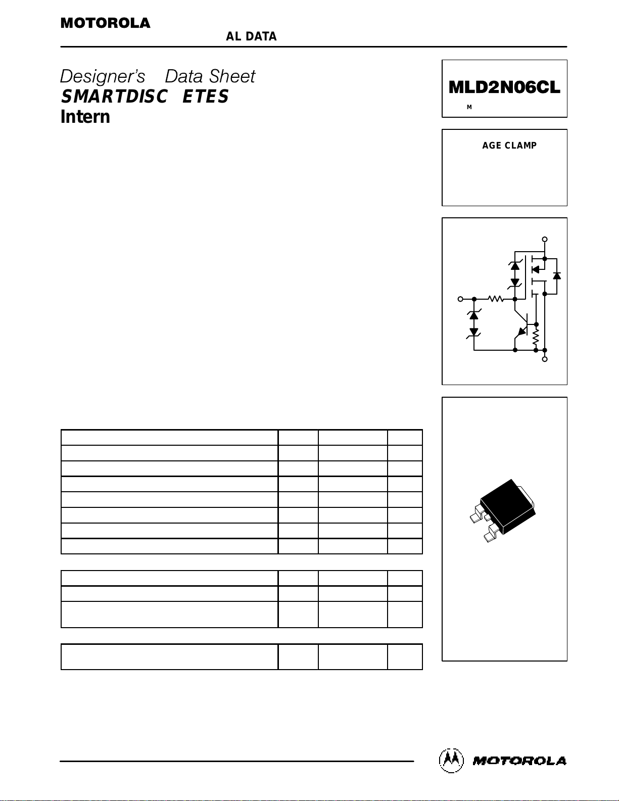
MLD2N06CL
Motorola Preferred Device
VOLTAGE CLAMPED
CURRENT LIMITING
MOSFET
62 VOLTS (CLAMPED)
R
DS(on)
= 0.4 OHMS
CASE 369A–13, Style 2
DPAK Surface Mount
D
G
S
R1
R2
Motorola, Inc. 1996
Page 2
MLD2N06CL
2
Motorola TMOS Power MOSFET Transistor Device Data
ELECTRICAL CHARACTERISTICS
(TC = 25°C unless otherwise noted)
Characteristic
Symbol Min Typ Max Unit
OFF CHARACTERISTICS
Drain–to–Source Breakdown Voltage
(ID = 20 mAdc, VGS = 0 Vdc)
(ID = 20 mAdc, VGS = 0 Vdc, TJ = 150°C)
V
(BR)DSS
58
58
62
62
66
66
Vdc
Zero Gate Voltage Drain Current
(VDS = 40 Vdc, VGS = 0 Vdc)
(VDS = 40 Vdc, VGS = 0 Vdc, TJ = 150°C)
I
DSS
—
—
0.6
6.0
5.0
20
µAdc
Gate–Source Leakage Current
(VG = 5.0 Vdc, VDS = 0 Vdc)
(VG = 5.0 Vdc, VDS = 0 Vdc, TJ = 150°C)
I
GSS
—
—
0.5
1.0
5.0
20
µAdc
ON CHARACTERISTICS(1)
Gate Threshold Voltage
(ID = 250 µAdc, VDS = VGS)
(ID = 250 µAdc, VDS = VGS, TJ = 150°C)
V
GS(th)
1.0
0.6
1.5
1
2.0
1.6
Vdc
Static Drain Current Limit
(VGS = 5.0 Vdc, VDS = 10 Vdc)
(VGS = 5.0 Vdc, VDS = 10 Vdc, TJ = 150°C)
I
D(lim)
3.8
1.6
4.4
2.4
5.2
2.9
Adc
Static Drain–to–Source On–Resistance
(ID = 1.0 Adc, VGS = 5.0 Vdc)
(ID = 1.0 Adc, VGS = 5.0 Vdc, TJ = 150°C)
R
DS(on)
—
—
0.3
0.53
0.4
0.7
Ohms
Forward Transconductance (ID = 1.0 Adc, VDS = 10 Vdc) g
FS
1.0 1.4 — mhos
Static Source–to–Drain Diode Voltage
(IS = 1.0 Adc, VGS = 0 Vdc)
V
SD
— 1.1 1.5
Vdc
SWITCHING CHARACTERISTICS(2)
Turn–On Delay Time
t
d(on)
— 1.0 1.5
µs
Rise Time
DD
= 30 Vdc, ID = 1.0 Adc,
t
r
— 3.0 5.0
Turn–Off Delay Time
(VDD = 30 Vdc, ID = 1.0 Adc,
V
GS(on)
= 5.0 Vdc, RGS = 25 Ohms)
t
d(off)
— 5.0 8.0
Fall Time t
f
— 3.0 5.0
(1) Pulse Test: Pulse Width ≤ 300 µs, Duty Cycle ≤ 2%.
(2) Switching characteristics are independent of operating junction temperature.
VDS, DRAIN–TO–SOURCE VOLTAGE (VOLTS)
I
D
, DRAIN CURRENT (AMPS)
I
D
, DRAIN CURRENT (AMPS)
VGS, GATE–TO–SOURCE VOLTAGE (VOLTS)
TJ = 25
°C
VDS ≥ 7.5 V
TJ = 150
°C
25
°C
–55
°C
0 1 2 3 8
2.5
2.0
1.5
1.0
0.5
0
3.0
3.5
4.0
4 5 6 7
0 2 4 6 8
5
4
3
2
1
0
6.0 V
5.5 V
5.0 V
4.5 V
4.0 V
3.5 V
3.0 V
2.5 V
2.0 V
(V
Figure 1. Output Characteristics Figure 2. Transfer Function
Page 3

MLD2N06CL
3
Motorola TMOS Power MOSFET Transistor Device Data
THE SMARTDISCRETES CONCEPT
From a standard power MOSFET process, several active
and passive elements can be obtained that provide on–chip
protection to the basic power device. Such elements require
only a small increase in silicon area and/or the addition of one
masking layer to the process. The resulting device exhibits
significant improvements in ruggedness and reliability as well
as system cost reduction. The SMARTDISCRETES device
functions can now provide an economical alternative to smart
power ICs for power applications requiring low on–resistance,
high voltage and high current.
These devices are designed for applications that require a
rugged power switching device with short circuit protection
that can be directly interfaced to a microcontroller unit (MCU).
Ideal applications include automotive fuel injector driver,
incandescent lamp driver or other applications where a high
in–rush current or a shorted load condition could occur.
OPERATION IN THE CURRENT LIMIT MODE
The amount of time that an unprotected device can withstand the current stress resulting from a shorted load before
its maximum junction temperature is exceeded is dependent
upon a number of factors that include the amount
of heatsinking that is provided, the size or rating of the device,
its initial junction temperature, and the supply voltage. Without
some form of current limiting, a shorted load can raise a device’s junction temperature beyond the maximum rated operating temperature in only a few milliseconds.
Even with no heatsink, the MLD2N06CL can withstand a
shorted load powered by an automotive battery (10 to 14
Volts) for almost a second if its initial operating temperature is
under 100°C. For longer periods of operation in the current–
limited mode, device heatsinking can extend operation from
several seconds to indefinitely depending on the amount of
heatsinking provided.
SHORT CIRCUIT PROTECTION AND THE EFFECT OF
TEMPERATURE
The on–chip circuitry of the MLD2N06CL offers an integrated
means of protecting the MOSFET component from high in–rush
current or a shorted load. As shown in the schematic diagram,
the current limiting feature is provided by an NPN transistor and
integral resistors R1 and R2. R2 senses the current through the
MOSFET and forward biases the NPN transistor’s base as the
current increases. As the NPN turns on, it begins to pull gate
drive current through R1, dropping the gate drive voltage across
it, and thus lowering the voltage across the gate–to–source of
the power MOSFET and limiting the current. The current limit is
temperature dependent as shown in Figure 3, and decreases
from about 2.3 Amps at 25°C to about 1.3 Amps at 150°C.
Since the MLD2N06CL continues to conduct current and dissipate power during a shorted load condition, it is important to
provide sufficient heatsinking to limit the device junction temperature to a m aximum of 150°C.
The metal current sense resistor R2 adds about 0.4 ohms to
the power MOSFET’s on–resistance, but the effect of temperature on the combination is less than on a standard MOSFET due
to the lower temperature coefficient of R2. The on–resistance
variation with temperature for gate voltages of 4 and 5 Volts is
shown in Figure 5.
Back–to–back polysilicon diodes between gate and source
provide ESD protection to greater than 2 kV, HBM. This on–chip
protection feature eliminates the need for an external Zener
diode for systems with potentially heavy line transients.
I
D(lim)
, DRAIN CURRENT (AMPS)
TJ, JUNCTION TEMPERATURE (°C)
VGS = 5 V
VDS = 10 V
–50 0 50 100 150
5
4
3
2
1
0
6
R
DS(on)
, ON–RESISTANCE (OHMS)
VGS, GATE–TO–SOURCE VOLTAGE (VOLTS)
ID = 1 A
0 1 2 3 9 10
1.0
0.8
0.6
0.4
0.2
0
4 5 6
7 8
TJ = –50
°C
100°C
25°C
R
DS(on)
, ON–RESISTANCE (OHMS)
TJ, JUNCTION TEMPERATURE (°C)
ID = 1 A
–50 500 100 150
0.6
0.4
0.3
0.2
0.1
0
0.5
VGS = 4 V
VGS = 5 V
Figure 3. I
With Temperature
Figure 4. R
DS(on)
Gate–To–Source Voltage
Figure 5. On–Resistance Variation With
Temperature
Variation
D(lim)
Variation With
Page 4

MLD2N06CL
4
Motorola TMOS Power MOSFET Transistor Device Data
TJ, STARTING JUNCTION TEMPERATURE (°C)
E
AS
, SINGLE PULSE DRAIN–TO–SOURCE
ID = 2 A
25 50 75 100 125 150
100
80
60
40
20
0
AVALANCHE ENERGY (mJ)
B
V(DSS)
, DRAIN–TO–SOURCE SUSTAINING
TJ = JUNCTION TEMPERATURE
–50 0 150
62.5
62.0
61.5
61.0
60.5
60.0
63.0
63.5
64.0
50 100
VOLTAGE (VOLTS)
ID = 20 mA
FORWARD BIASED SAFE OPERATING AREA
The FBSOA curves define the maximum drain–to–source
voltage and drain current that a device can safely handle
when it is forward biased, or when it is on, or being turned on.
Because these curves include the limitations of simultaneous
high voltage and high current, up to the rating of the device,
they are especially useful to designers of linear systems. The
curves are based on a case temperature of 25°C and a maximum junction temperature of 150°C. Limitations for repetitive
pulses at various case temperatures can be determined by
using the thermal response curves. Motorola A pplication
Note, AN569, “Transient Thermal Resistance — General
Data and Its Use” provides detailed instructions.
MAXIMUM DC VOLTAGE CONSIDERATIONS
The maximum drain–to–source voltage that can be continuously applied across the MLD2N06CL when it is in current
limit is a function of the power that must be dissipated. This
power is determined by the maximum current limit at maximum rated operating temperature (1.8 A at 150°C) and not
the R
DS(on)
. The maximum voltage can be calculated by the
following equation:
where the value of R
θCA
is determined by the heatsink that is
being used in the application.
DUTY CYCLE OPERATION
When operating in the duty cycle mode, the maximum
drain voltage can be increased. The maximum operating
temperature is related to the duty cycle (DC) by the following
equation:
TC = (VDS x ID x DC x R
θCA
) + T
A
The maximum value of VDS applied when operating in a
duty cycle mode can be approximated by:
VDS =
150 – T
C
I
D(lim)
x DC x R
θJC
Figure 8. Maximum Rated Forward Bias
Safe Operating Area (MLD2N06CL)
VDS, DRAIN–TO–SOURCE VOLTAGE (VOLTS)
, DRAIN CURRENT (AMPS)
VGS = 10 V
SINGLE PULSE
TC = 25°C
dc
10 ms
100101.00.1
0.1
1.0
10
1 ms
R
DS(on)
LIMIT
THERMAL LIMIT
PACKAGE LIMIT
I
D
Figure 6. Maximum Avalanche Energy
versus Starting Junction Temperature
V
supply
=
(150 – TA)
I
(R
D(lim)
+ R
θJC
θCA
)
Figure 7. Drain–Source Sustaining
Voltage Variation With Temperature
Page 5

MLD2N06CL
5
Motorola TMOS Power MOSFET Transistor Device Data
Figure 9. Thermal Response (MLD2N06CL)
t, TIME (s)
r(t), NORMALIZED EFFECTIVE
TRANSIENT THERMAL RESISTANCE
R
θ
JC
(t) = r(t) R
θ
JC
D CURVES APPLY FOR POWER
PULSE TRAIN SHOWN
READ TIME AT t
1
T
J(pk)
– TC = P
(pk)
R
θ
JC
(t)
P
(pk)
t
1
t
2
DUTY CYCLE, D = t1/t
2
0.01
0.1
1.0
1.0E–05 1.0E–04 1.0E– 03 1.0E–02 1.0E–01 1.0E+00 1.0E+01
D = 0.5
0.02
0.2
0.05
0.1
SINGLE PULSE
0.01
PULSE GENERATOR
V
DD
V
out
V
in
R
gen
50
Ω
z = 50
Ω
50
Ω
DUT
R
L
Figure 10. Switching Test Circuit
t
off
OUTPUT, V
out
INVERTED
t
on
t
r
t
d(off)
t
f
t
d(on)
90%90%
10%
INPUT, V
in
10%
50%
90%
50%
PULSE WIDTH
Figure 11. Switching Waveforms
ACTIVE CLAMPING
SMARTDISCRETES technology can provide on–chip realization of the popular gate–to–source and gate–to–drain
Zener diode clamp elements. Until recently, such features
have been i mplemented only with d iscrete components
which consume board space and add system cost. The
SMARTDISCRETES technology approach economically
melds these features and the power chip with only a slight
increase in chip area.
In practice, back–to–back diode elements are formed in a
polysilicon region monolithicly integrated with, but electrically
isolated from, the main device structure. Each back–to–back
diode element provides a temperature compensated voltage
element of about 7 .2 volts. A s the polysilicon r egion is
formed on top of silicon dioxide, the diode elements are free
from direct interaction with the conduction regions of the
power d evice, thus eliminating parasitic e lectrical effects
while maintaining excellent thermal coupling.
To achieve high gate–to–drain clamp voltages, several
voltage elements are strung together; the MLD2N06CL uses
8 such elements. Customarily, two voltage elements are
used to provide a 14.4 volt gate–to–source voltage clamp.
For the MLD2N06CL, the integrated gate–to–source voltage
elements provide greater than 2.0 kV electrostatic voltage
protection.
The avalanche voltage of the gate–to–drain voltage clamp
is set less than that of the power MOSFET device. As soon
as the drain–to–source voltage exceeds this avalanche voltage, the resulting gate–to–drain Zener current builds a gate
voltage across the gate–to–source impedance, turning on
the power device which then conducts the current. Since virtually all of the current is carried by the power device, the
gate–to–drain voltage clamp element may be small in size.
This technique of establishing a temperature compensated
drain–to–source sustaining voltage (Figure 7) effectively removes the possibility of drain–to–source avalanche in the
power device.
The gate–to–drain voltage clamp technique is particularly
useful for snubbing loads where the inductive energy would
otherwise avalanche the power device. An improvement in
ruggedness of at least four times has been observed when
inductive energy is dissipated in the gate–to–drain clamped
conduction mode rather than in the more stressful gate–to–
source avalanche mode.
Page 6

MLD2N06CL
6
Motorola TMOS Power MOSFET Transistor Device Data
TYPICAL APPLICATIONS: INJECTOR DRIVER, SOLENOIDS, LAMPS, RELAY COILS
The MLD2N06CL has been designed to allow direct interface to the output of a microcontrol unit to control an isolated
load. No additional series gate resistance is required, but a
40 kΩ gate pulldown resistor is recommended to avoid a
floating gate condition in the event of an MCU failure. The internal clamps allow the device to be used without any external transistent suppressing components.
V
DD
V
BAT
MLD2N06CL
G
D
S
MCU
PACKAGE DIMENSIONS
CASE 369A–13
ISSUE W
D
A
K
B
R
V
S
F
L
G
2 PL
M
0.13 (0.005) T
E
C
U
J
H
–T–
SEATING
PLANE
Z
DIM MIN MAX MIN MAX
MILLIMETERSINCHES
A 0.235 0.250 5.97 6.35
B 0.250 0.265 6.35 6.73
C 0.086 0.094 2.19 2.38
D 0.027 0.035 0.69 0.88
E 0.033 0.040 0.84 1.01
F 0.037 0.047 0.94 1.19
G 0.180 BSC 4.58 BSC
H 0.034 0.040 0.87 1.01
J 0.018 0.023 0.46 0.58
K 0.102 0.114 2.60 2.89
L 0.090 BSC 2.29 BSC
R 0.175 0.215 4.45 5.46
S 0.020 0.050 0.51 1.27
U 0.020 ––– 0.51 –––
V 0.030 0.050 0.77 1.27
Z 0.138 ––– 3.51 –––
NOTES:
1. DIMENSIONING AND TOLERANCING PER ANSI
Y14.5M, 1982.
2. CONTROLLING DIMENSION: INCH.
1 2 3
4
STYLE 2:
PIN 1. GATE
2. DRAIN
3. SOURCE
4. DRAIN
How to reach us:
USA /EUROPE: Motorola Literature Distribution; JAPAN: Nippon Motorola Ltd.; Tatsumi–SPD–JLDC, Toshikatsu Otsuki,
P.O. Box 20912; Phoenix, Arizona 85036. 1–800–441–2447 6F Seibu–Butsuryu–Center, 3–14–2 Tatsumi Koto–Ku, Tokyo 135, Japan. 03–3521–8315
MFAX: RMFAX0@email.sps.mot.com – TOUCHTONE (602) 244–6609 HONG KONG: Motorola Semiconductors H.K. Ltd.; 8B Tai Ping Industrial Park,
INTERNET: http://Design–NET.com 51 Ting Kok Road, Tai Po, N.T., Hong Kong. 852–26629298
Motorola reserves the right to make changes without further notice to any products herein. Motorola makes no warranty , representation or guarantee regarding
the suitability of its products for any particular purpose, nor does Motorola assume any liability arising out of the application or use of any product or circuit,
and specifically disclaims any and all liability, including without limitation consequential or incidental damages. “T ypical” parameters can and do vary in different
applications. All operating parameters, including “T ypicals” must be validated for each customer application by customer’s technical experts. Motorola does
not convey any license under its patent rights nor the rights of others. Motorola products are not designed, intended, or authorized for use as components in
systems intended for surgical implant into the body, or other applications intended to support or sustain life, or for any other application in which the failure of
the Motorola product could create a situation where personal injury or death may occur. Should Buyer purchase or use Motorola products for any such
unintended or unauthorized application, Buyer shall indemnify and hold Motorola and its officers, employees, subsidiaries, affiliates, and distributors harmless
against all claims, costs, damages, and expenses, and reasonable attorney fees arising out of, directly or indirectly, any claim of personal injury or death
associated with such unintended or unauthorized use, even if such claim alleges that Motorola was negligent regarding the design or manufacture of the part.
Motorola and are registered trademarks of Motorola, Inc. Motorola, Inc. is an Equal Opportunity/Affirmative Action Employer.
MLD2N06CL/D
*MLD2N06CL/D*
◊
 Loading...