

Page 1

Preliminary
PEDL9090-02
This version: Jan. 2000
¡ Semiconductor
Previous version: Nov. 1998
ML9090-01,-02
LCD Driver with Key Scanner and RAM
GENERAL DESCRIPTION
The ML9090-01 and ML9090-02 are LCD drivers that contain internal RAM and a key scan
function. They are best suited for car audio displays.
Since 1-bit data of the display RAM corresponds to the light-on or light-off of 1-dot of the LCD
panel (a bit map system), a flexible display is possible.
A single chip can implement a graphic display system of a maximum of 80 ¥ 16 dots (80 ¥ 8 dots
for the ML9090-01, 80 ¥ 16 dots for the ML9090-02) and an arbitrator display system of 80 ¥ 2 dots.
Since containing voltage multipliers, the ML9090-01 and ML9090-02 require no power supply
circuit to drive the LCD.
Since the internal 5 ¥ 5 scan circuit has eliminated the needs of key scanning by the CPU, the ports
of the CPU can be efficiently used.
FEATURES
• Logic voltage: VDD 2.7 to 5.5 V
• LCD drive voltage: VBI 6 to 16 V (positive voltage)
• 80 segment outputs,10 common outputs for ML9090-01 and 18 common outputs for ML909002
• Built-in bit-mapped RAM (ML9090-01: 80 ¥ 10 = 800 bits, ML9090-02: 80 ¥ 18 = 1440 bits)
• 4-pin serial interface with CPU: CS, CP, DI/O, KREQ
• Built-in LCD drive bias resistors
• Built-in voltage doubler and tripler circuits
• Built-in 5 ¥ 5 key scanner
• Port A output : 1 pin, output current: -15mA: (may be used for LED driving)
• Port B output : 8 pins
Output current (available for the ML9090-01 only)
–2mA : 5 pins
–15mA : 3 pins
• Temperature range: –40 to +85˚C
• Package: 128-pin plastic QFP (QFP128-P-1420-0.50-K) (Product name: ML9090-01GA)
(Product name: ML9090-02GA)
Model ML9090-01 ML9090-02
Display duty 1/8 1/9 1/10 1/16 1/17 1/18
No. of display lines 8 9 10 16 17 18
No. of port B outputs 8 8 8 — — —
APPLICATION
• Car audio
1/38
Page 2
PEDL9090-02
¡ Semiconductor ML9090-01,-02
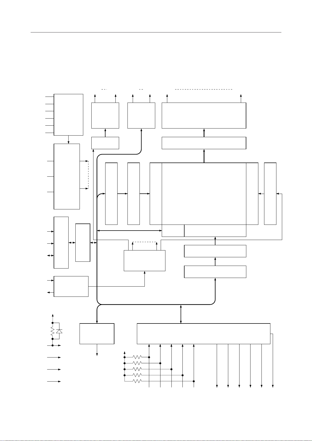
BLOCK DIAGRAM
ML9090-01
COM1
V
IN
V
C1
V
C2
V
S1
V
S2
VOLTAGE
DOUBLER/
TRIPLER
10-OUT
COMMON
DRIVER
PB0 SEG1COM10 PB7 SEG80
8-PORT
80-OUT SEGMENT DRIVER
DRIVER
DT
SHIFT
REGISTER
DATA LATCH
LCD BIAS
V
2
VOLTAGE
V
3B
DIVIDING
V
3A
CS
CIRCUIT
Y ADDRESS REGISER
Y ADDRESS COUNTER
Y ADDRESS DECODER
BUFFER
DISPLAY DATA RAM
80 ¥ 10 BITS
I/O
X ADDRESS DECODER
LINE ADDRESS DECODER
DISPLAY LINE COUNTER
CP
DI/O
OSC1
OSC2
RESET
TEST
V
DD
V
SS
CONTROL
INTERFACE
INPUT OUTPUT
OSCILLATION
CIRCUIT
REGISTER
1 PORT
DRIVER
PA0
X ADDRESS COUNTER
TIMING
GENERATOR
X ADDRESS REGISTER
5 ¥ 5
KEY SCANNER
CO C1 C2 C3 C4 R0 R1 R2 R3
R4 KREQ
2/38
Page 3
PEDL9090-02
¡ Semiconductor ML9090-01,-02
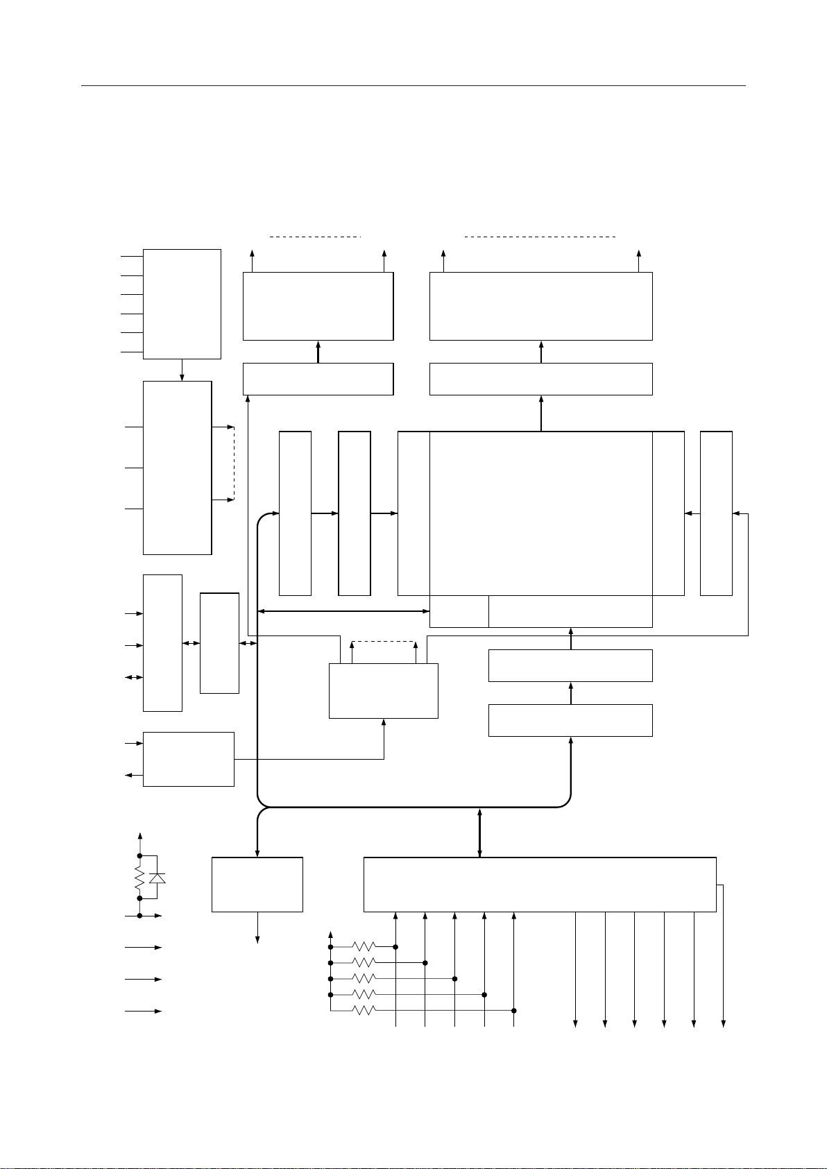
BLOCK DIAGRAM
ML9090-02
COM1 SEG1COM18 SEG80
V
IN
V
V
V
V
C1
C2
S1
S2
DT
VOLTAGE
DOUBLER/
TRIPLER
18-OUT
COMMON DRIVER
80-OUT SEGMENT DRIVER
DATA LATCHSHIFT REGISTER
V
V
3B
V
3A
CS
CP
DI/O
OSC1
OSC2
2
LCD BIAS
VOLTAGE
DIVIDING
CIRCUIT
CONTROL
INTERFACE
INPUT OUTPUT
OSCILLATION
CIRCUIT
REGISTER
Y ADDRESS REGISER
Y ADDRESS COUNTER
TIMING
GENERATOR
DISPLAY DATA RAM
80 ¥ 18 BITS
Y ADDRESS DECODER
I/O
BUFFER
X ADDRESS DECODER
X ADDRESS COUNTER
X ADDRESS REGISTER
LINE ADDRESS DECODER
DISPLAY LINE COUNTER
RESET
TEST
V
DD
V
SS
1 PORT
DRIVER
PA0
5 ¥ 5
KEY SCANNER
CO C1 C2 C3 C4 R0 R1 R2 R3
R4 KREQ
3/38
Page 4
PEDL9090-02
¡ Semiconductor ML9090-01,-02
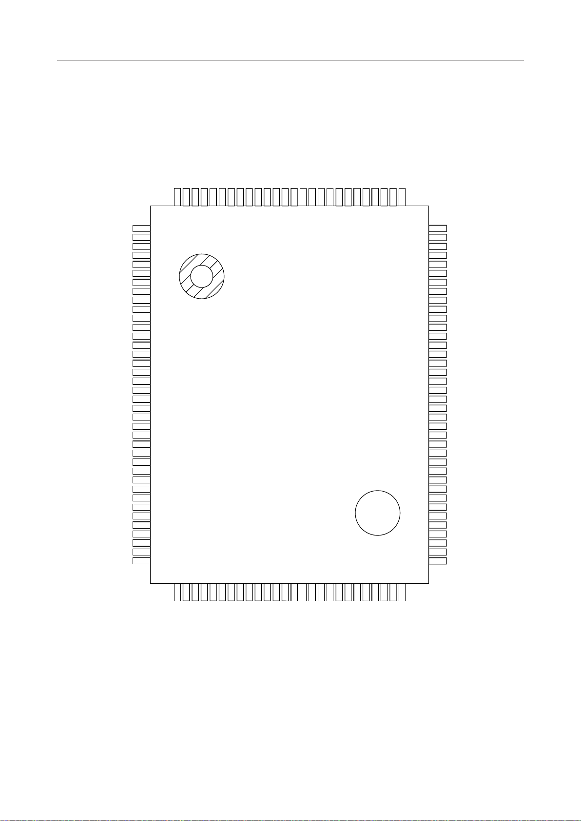
PIN CONFIGURATION (TOP VIEW)
ML9090-01
SEG74
SEG75
SEG76
SEG77
SEG78
SEG79
SEG80
COM1
COM2
COM3
COM4
COM5
COM6
COM7
COM8
COM9
COM10
PB0
PB1
PB2
PB3
PB4
PB7
PA0
PB5
PB6
128
127
126
125
124
123
122
121
120
119
118
117
116
115
114
113
112
111
110
109
108
107
106
105
104
103
SEG73
SEG72
SEG71
SEG70
SEG69
SEG68
SEG67
SEG66
SEG65
SEG64
SEG63
SEG62
SEG61
SEG60
SEG59
SEG58
SEG57
SEG56
SEG55
SEG54
SEG53
SEG52
SEG51
SEG50
SEG49
SEG48
SEG47
SEG46
SEG45
SEG44
SEG43
SEG42
SEG41
SEG40
SEG39
SEG38
SEG37
SEG36
1
2
3
4
5
6
7
8
9
10
11
12
13
14
15
16
17
18
19
20
21
22
23
24
25
26
27
28
29
30
31
32
33
34
35
36
37
38
102
101
100
99
98
97
96
95
94
93
92
91
90
89
88
87
86
85
84
83
82
81
80
79
78
77
76
75
74
73
72
71
70
69
68
67
66
65
V
DD
OSC2
OSC1
DT
V
2
V
3B
V
3A
V
IN
V
C1
V
C2
V
S1
V
S2
V
SS
TEST
RESET
KREQ
DI/O
CS
CP
C0
C1
C2
C3
C4
R0
R1
R2
R3
R4
SEG1
SEG2
SEG3
SEG4
SEG5
SEG6
SEG7
SEG8
SEG9
394041
SEG35
SEG34
SEG33
42434445464748
SEG31
SEG30
SEG29
SEG28
SEG32
SEG27
128-Pin Plastic QFP
49
50515253545556
SEG26
SEG25
SEG24
SEG23
SEG22
SEG21
SEG20
SEG19
57
58596061626364
SEG18
SEG17
SEG16
SEG15
SEG14
SEG13
SEG12
SEG11
SEG10
4/38
Page 5
PEDL9090-02
¡ Semiconductor ML9090-01,-02
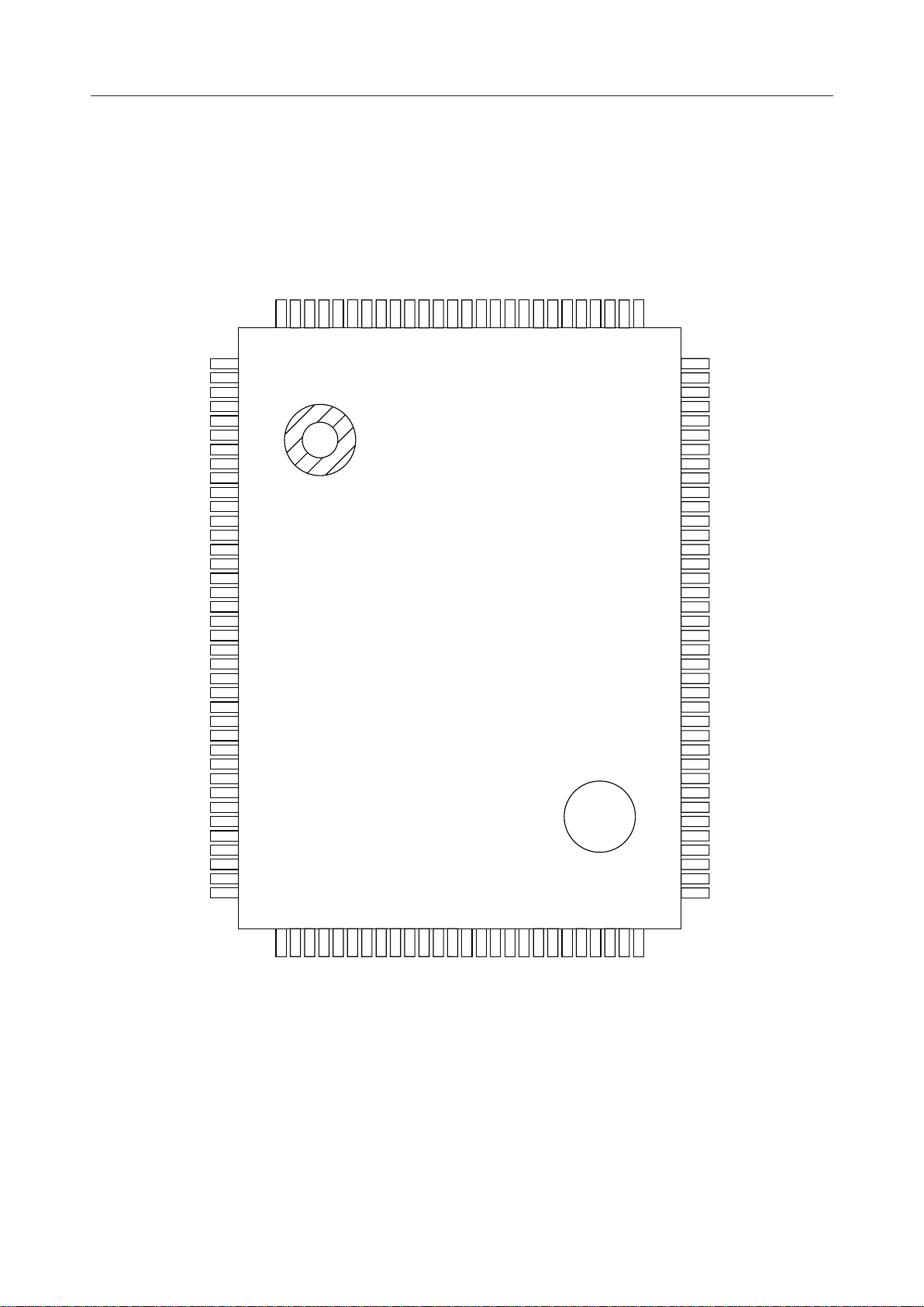
PIN CONFIGURATION (TOP VIEW)
ML9090-02
SEG74
SEG75
SEG76
SEG77
SEG78
SEG79
SEG80
COM1
COM2
COM3
COM4
COM5
COM6
COM7
COM8
COM9
COM10
COM11
COM12
COM13
COM14
COM15
COM18
PA0
COM16
COM17
128
127
126
125
124
123
122
121
120
119
118
117
116
115
114
113
112
111
110
109
108
107
106
105
104
103
SEG73
SEG72
SEG71
SEG70
SEG69
SEG68
SEG67
SEG66
SEG65
SEG64
SEG63
SEG62
SEG61
SEG60
SEG59
SEG58
SEG57
SEG56
SEG55
SEG54
SEG53
SEG52
SEG51
SEG50
SEG49
SEG48
SEG47
SEG46
SEG45
SEG44
SEG43
SEG42
SEG41
SEG40
SEG39
SEG38
SEG37
SEG36
1
2
3
4
5
6
7
8
9
10
11
12
13
14
15
16
17
18
19
20
21
22
23
24
25
26
27
28
29
30
31
32
33
34
35
36
37
38
102
101
100
99
98
97
96
95
94
93
92
91
90
89
88
87
86
85
84
83
82
81
80
79
78
77
76
75
74
73
72
71
70
69
68
67
66
65
V
DD
OSC2
OSC1
DT
V
2
V
3B
V
3A
V
IN
V
C1
V
C2
V
S1
V
S2
V
SS
TEST
RESET
KREQ
DI/O
CS
CP
C0
C1
C2
C3
C4
R0
R1
R2
R3
R4
SEG1
SEG2
SEG3
SEG4
SEG5
SEG6
SEG7
SEG8
SEG9
394041
SEG35
SEG34
SEG33
42434445464748
SEG31
SEG30
SEG29
SEG28
SEG32
SEG27
128-Pin Plastic QFP
49
50515253545556
SEG26
SEG25
SEG24
SEG23
SEG22
SEG21
SEG20
SEG19
57
58596061626364
SEG18
SEG17
SEG16
SEG15
SEG14
SEG13
SEG12
SEG11
SEG10
5/38
Page 6
PEDL9090-02
¡ Semiconductor ML9090-01,-02
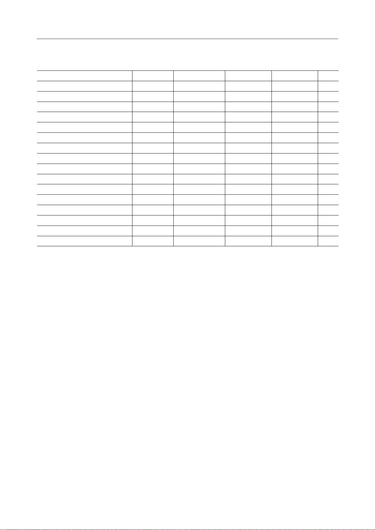
ABSOLUTE MAXIMUM RATINGS
Parameter
Power Supply Voltage
Bias Voltage V
Voltage Multiplier Reference
Voltage
Symbol
V
DD
BI
V
IN
Condition
Ta = 25°C
Rating
–0.3 to +7.0
Ta = 25°C –0.3 to +18.0 V
Ta = 25°C –0.3 to +9.84
Ta = 25°C*1*2 –0.3 to +7.36
UnitVApplicable Pins
V
DD
, VC2, VS1,
V
C1
, V2, V3A, V
V
S2
VV
3B
IN
CS, CP, DI/O,
Input Voltage V
I
Ta = 25°C –0.3 to VDD+0.3 V
OSC1, RESET, DT,
TEST, C0 to C4
Ta = 25°C –20 mA PA0, PB5 to PB7
Output Current I
Power Dissipation P
Storage Temperature T
O
stg
Ta = 25°C –3 mA PB0 to PB4
D
Ta = 85°C 190 mW —
— –55 to +150 ˚C —
*1: When Ta = 25˚C and the voltage doubler is used, use voltage multiplier reference
voltage VIN values within a range that does not exceed the maximum bias voltage.
*2: When Ta = 25˚C and the voltage tripler is used, use voltage multiplier reference voltage
VIN values within a range that does not exceed the maximum bias voltage.
RECOMMENDED OPERATING CONDITIONS
Parameter
Power Supply Voltage
Bias Voltage V
Voltage Multiplier Reference
Voltage
Operating Frequency F
Operating Temperature T
*1: For the bias voltage, VS2 is the maximum voltage potential and VSS is the minimum
voltage potential. VS2 > V
*2: When the voltage doubler is used, use voltage multiplier reference voltage VIN values
within a range that does not exceed the maximum bias voltage.
*3: When the voltage tripler is used, use voltage multiplier reference voltage VIN values
within a range that does not exceed the maximum bias voltage.
Symbol
V
DD
BI
V
IN
op
op
≥ V
2
Condition
—
Range
2.7 to 5.5
UnitVApplicable Pins
*1 6.0 to 16.0 V V
*2 3.0 to 8.8
VV
*3 2.0 to 6.6
R = 56kW ±2% 480 to 1200 kHz OSC1
— –40 to +85 ˚C —
, V3B > VSS.
3A
V
DD
S2
IN
6/38
Page 7
PEDL9090-02
¡ Semiconductor ML9090-01,-02
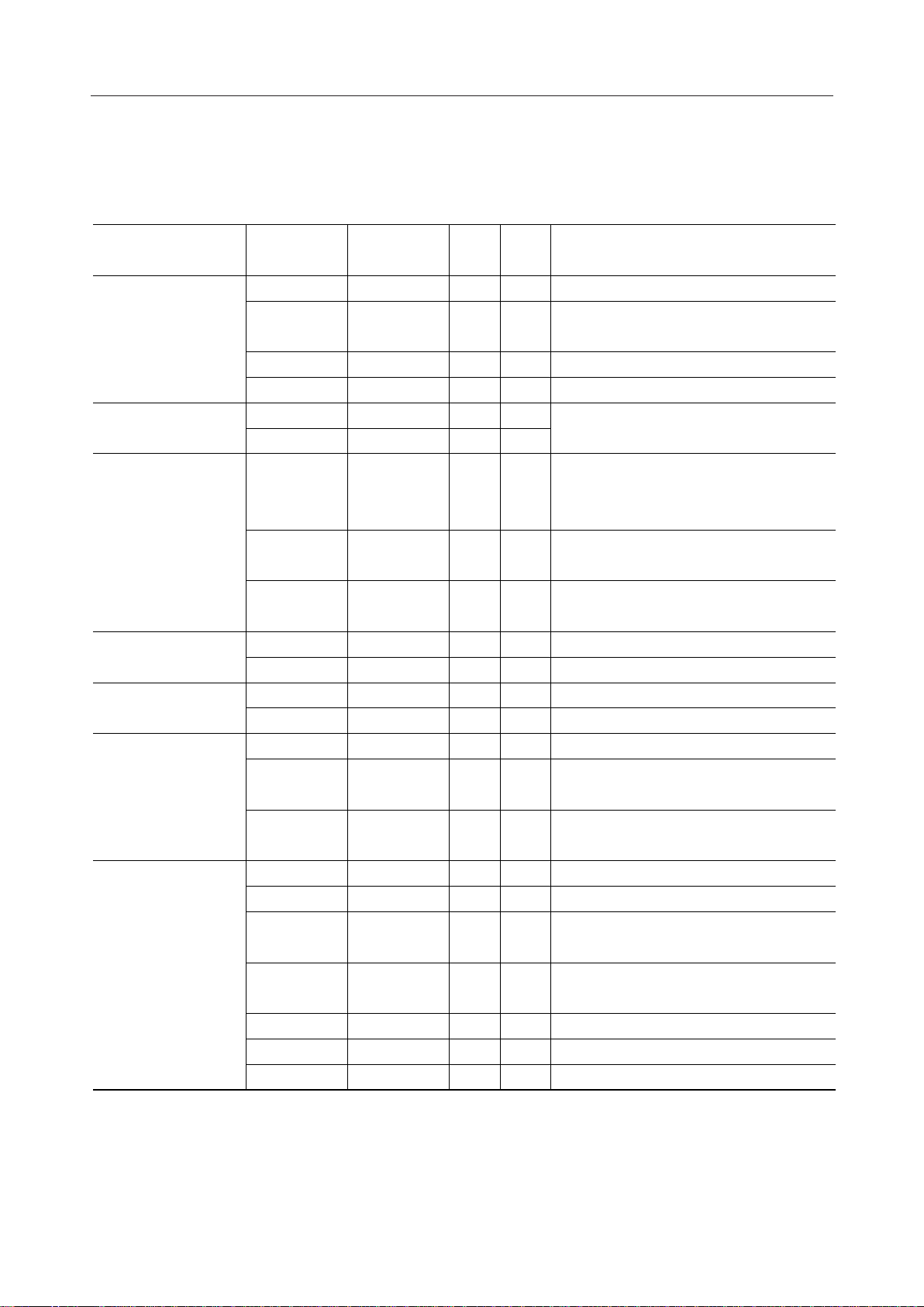
ELECTRICAL CHARACTERISTICS
DC Characteristics
(V
= 2.7 to 5.5 V, VBI = 6 to 16 V, Ta = –40 to +85˚C)
DD
Parameter
"H" Input Voltage 1
"H" Input Voltage 2 V
"H" Input Voltage 3 V
"H" Input Voltage 4 V
"L" Input Voltage 1 V
"L" Input Voltage 2 V
"L" Input Voltage 3 V
"L" Input Voltage 4 V
Hysteresis Voltage 1 V
Hysteresis Voltage 2 V
Hysteresis Voltage 3 V
"H" Input Current 1 I
"H" Input Current 2 I
"H" Input Current 3 I
"H" Input Current 4 I
"L" Input Current 1 I
"L" Input Current 2 I
"L" Input Current 3 I
"L" Input Current 4 I
"H" Output Voltage 1 V
"H" Output Voltage 2 V
"H" Output Voltage 3 V
"H" Output Voltage 4 V
"H" Output Voltage 5 V
"L" Output Voltage 1 V
"L" Output Voltage 2 V
"L" Output Voltage 3 V
"L" Output Voltage 4 V
LCD Driving Bias Resistance L
Segment Output Voltage 1
(1/4 bias)
Symbol
V
IH1
IH2
IH3
IH4
IL1
IL2
IL3
IL4
HIS1
HIS2
HIS3
IH1
IH2
IH3
IH4
IL1
IL2
IL3
IL4
OH1
OH2
OH3
OH4
OH5
OL1
OL2
OL3
OL4
BR
V
OS0
V
OS1
V
OS2
V
OS3
Condition—Min.
0.85V
— 0.85V
— 0.85V
Typ.—Max.
DD
—VDDV RESET
DD
—VDDV CP
DD
V
UnitVApplicable Pins
DD
OSC1
CS, DI/O,
— 0.8V
DD
— 0 — 0.15V
— 0 — 0.15V
— 0 — 0.15V
—VDDV
DD
DD
DD
C0 to C4
V OSC1
V RESET
V CP
CS, DI/O,
— 0 — 0.2V
DD
V
C0 to C4
VDD = 5 V — 0.3 — V OSC1
VDD = 5 V — 0.4 — V CP
VDD = 5 V — 0.4 — V RESET
VI = V
VI = V
VI = V
DD
DD
DD
——10mA RESET
——10mAC0 to C4
——10mA DI/O
OSC1, CS, CP,
VI = V
DD
VDD = 5 V, VI = 0 V
VDD = 5 V, VI = 0 V
VI = 0 V
—— 1mA
DT, TEST
–0.02 –0.05 –0.1 mA RESET
–0.18 –0.45 –0.9 mA C0 to C4
—
— –10 mA DI/O
OSC1, CS, CP,
VI = 0 V
—–1mA
—
DT, TEST
V
IO = –0.4mA
IO = –40mA
IO = –15mA
IO = –2mA — — V PB0 to PB4
IO = –50mA——VR0 to R4
DD
0.9V
V
DD
V
DD
V
DD
–0.4
DD
–1.7
–1.2
–2.0
— — V DI/O, KREQ
— — V OSC2
— — V PA0, PB5 to PB7
IO = 0.4mA — — 0.4 V DI/O, KREQ
IO = 40mA — — 0.1V
V OSC2
DD
IO = 1mA — — 0.4 V PA0, PB0 to PB7
IO = 1.8mA — — 0.7 V R0 to R4
— 6.3 9 13 kW V2 to V
IO = –10mAVS2–0.6 — — V
IO = ±10mA
2/4VS2–0.6
—
2/4VS2+0.6
V
SEG1 to SEG80
IO = ±10mA
2/4VS2–0.6
—
2/4VS2+0.6
V
IO = +10mA— —VSS+0.6 V
3A
7/38
Page 8
PEDL9090-02
¡ Semiconductor ML9090-01,-02
(VDD = 2.7 to 5.5 V, VBI = 6 to 16 V, Ta = –40 to +85˚C)
Parameter Symbol Condition Min. Typ. Max. Unit
Common Output Voltage 1
(1/4 bias)
Segment Output Voltage 2
(1/5 bias)
Common Output Voltage 2
(1/5 bias)
Voltage Multiplier Voltage 1 V
Voltage Multiplier Voltage 2 V
Supply Current 1 I
Supply Current 2 I
V
OC0
V
OC1
V
OC2
V
OC3
V
OS0
V
OS1
V
OS2
V
OS3
V
OC0
V
OC1
V
OC2
V
OC3
IO = –10mAVS2–0.3 — — V
IO = ±10mA
IO = ±10mA
IO = +10mA— —VSS+0.3 V
IO = –10mAVS2–0.6 — — V
IO = ±10mA
IO = ±10mA
IO = +10mA— —VSS+0.6 V
IO = –10mAVS2–0.3 — — V
IO = ±10mA
IO = ±10mA
IO = +10mA— —VSS+0.3 V
External clock
DB
= 740KHz *1
External clock
TR
= 740KHz *1
R = 56KW
DD1
*1
External clock
DD2
= 740KHz *1
±2%
3/4VS2–0.3
1/4VS2–0.3
3/5VS2–0.6
2/5VS2–0.6
4/5VS2–0.3
1/5VS2–0.3
—V
3/4VS2+0.3
—V
—V
—V
—V
—V
1/4V
3/5V
2/5V
4/5V
1/5V
S2
S2
S2
S2
S2
+0.3
+0.6
+0.6
+0.3
+0.3
VIN¥1.83
——V V
–0.5
VIN¥2.46
——V V
–1.0
— — 0.95 mA V
— — 0.7 mA V
Applicable Pins
C0M1 to C0M18
SEG1 to SEG80
C0M1 to C0M18
S1
S2
DD
DD
*1: Refer to Measuring Circuits
8/38
Page 9
PEDL9090-02
¡ Semiconductor ML9090-01,-02
Measuring Circuits
VDB
2.5-8V
V
2.7-5.5V
4.7mF
4.7mF
+
100mA
–
+
OPEN
Voltage multiplier voltage 1
When voltage doubler is used.
OPEN
SEG1 - SEG80 COM1 - COM10
V
DD
V
IN
V
C1
V
C2
V
S1
V
S2
PAO
OSC2
DT
OSC1
V
2
V
3B
V
3A
CS
CP
DI/O
*1
COM11 - COM18/
PB0 - PB7
C0 - C4 R0 - R4
TEST
RESET V
OPEN
V
SS
OPEN
OPEN
f = 740kHz
DD
2.5-7V
VDR
V
2.7-5.5V
4.7mF
100mA
–
+
4.7mF
+
4.7mF
+
OPEN
Voltage multiplier voltage 2
When voltage tripler is used.
OPEN
V
SEG1 - SEG80 COM1 - COM10
DD
V
IN
V
C1
V
C2
V
S1
V
S2
DTVDD
V
2
V
3B
V
3A
CS
CP
DI/O
*1
COM11 - COM18/
PB0 - PB7
RESET V
C0 - C4 R0 - R4
OPEN
V
SS
PAO
OSC2
OSC1
TEST
OPEN
OPEN
f = 740kHz
DD
5.5V
6.0V
IDDI
A
4.7mF
–
+
4.7mF
+
4.7mF
+
OPEN
Supply current 1
OPEN
SEG1 - SEG80 COM1 - COM10
V
DD
V
IN
V
C1
V
C2
V
S1
V
S2
DTVDD
V
2
V
3B
V
3A
CS
CP
DI/O
*1
COM11 - COM18/
PB0 - PB7
C0 - C4 R0 - R4
OPEN
V
SS
OPEN
PAO
OSC2
OSC1
TEST
RESET V
5.5V
6.0V
R = 56kW
±2%
DD
IDD2
A
4.7mF
–
+
4.7mF
+
4.7mF
+
OPEN
Supply current 2
OPEN
SEG1 - SEG80 COM1 - COM10
V
DD
V
IN
V
C1
V
C2
V
S1
V
S2
DTVDD
V
2
V
3B
V
3A
CS
CP
DI/O
*1
COM11 - COM18/
PB0 - PB7
C0 - C4 R0 - R4
OPEN
V
SS
OPEN
PAO
OSC2
OPEN
OSC1
f = 740kHz
TEST
RESET V
DD
*1: PB0 - PB7 for ML9090-01, and COM11 - COM18 for ML9090-02
9/38
Page 10
PEDL9090-02
¡ Semiconductor ML9090-01,-02
Switching Characteristics
= 2.7 to 5.5 V, VBI = 6 to 16 V, Ta = –40 to +85˚C)
(V
DD
Parameter
CP Clock Cycle Time
CP "H" Pulse Width t
CP "L" Pulse Width t
CS "H" Pulse Width t
CP Clock Rise/fall Time tr, t
CS Setup Time t
CS Hold Time t
DI/O Setup Time t
DI/O Hold Time t
DI/O Output Delay Time t
DI/O Output OFF Delay Time t
RESET Pulse Width t
External Clock Cycle Time t
External Clock "H" Pulse Width t
External Clock "L" Pulse Width t
External Clock Rise/fall Time trE, t
Symbol
t
SYS
WH
WL
WCH
f
CSU
CHD
DSU
DHD
DOD
DOFF
WRE
SES
WEH
WEL
fE
Condition
—
—ns400
—ns400
—ns200
—ns—
—ns60
—ns290
—ns100
—ns15
CL = 50pF ns—
CL = 50pF ns—
Min
1000
Max
—
—
—
—
100
—
—
—
—
200
200
Unit
ns
— ms2
—ns833
—ns316
—ns316
—ns—
—
—
—
100
10/38
Page 11

PEDL9090-02
¡ Semiconductor ML9090-01,-02
Clock synchronous serial interface timing diagrams
Clock synchronous serial interface input timing
CS
CP
DI-O
V
IL4
t
CSU
r
V
IH3
V
IL3
t
DSU
V
IH4
V
IL4
t
SYS
IH3
V
IL3
DHD
V
t
t
WL
r
V
IH3
V
IL3
IH4
V
IL4
tWHt
V
V
IH3
t
Clock synchronous serial interface input/output timing
CS
V
IL4
t
CSU
t
SYS
t
WCH
V
IH4
CHD
V
t
WCH
V
IH4
IL4
V
IH4
V
IH4
V
t
CHD
V
IH3
IL4
t
CP
DI-O
Reset timing
RESET
External clock
V
t
DHD
t
t
WL
r
8 Clock
IH3
V
IL3
V
IL4
V
IL2
t
t
WEH
rE
V
IH3
V
IL3
t
t
WEL
rE
V
IL3
t
DOD
V
OH1
V
Hiz
OL1
V
IH3
t
DOFF
V
OH1
V
OL1
tWHt
r
1 Clock
V
IL3
t
V
IH3
V
IH4VIH4
V
IL4
WRE
V
IH3
t
DSU
V
IL2
OSC1
V
V
IL1
IH1VIH1
t
V
SES
IL1
V
IL1
11/38
Page 12
PEDL9090-02
¡ Semiconductor ML9090-01,-02
FUNCTIONAL DESCRIPTIONS
Pin Functional Descriptions
Function Symbol Pin name Type
CS Chip Select I 1 Chip select signal input pin
CP Clock Pulse I 1
CPU interface
DI/O Data I/O I/O 1 Serial data signal I/O pin
KREQ Key Request O 1 Key request signal output pin
OSC1 OSC1 I 1
Oscillation
OSC2 OSC2 O 1
RESET RESET I 1
Control signals
Doubler Tripler
DT
Select
TEST TEST I 1
C0 to C4 Column Input I 5
Key scan signals
R0 to R4 Row Output O 5 Key switch scan signal pins
PA0 Port Output O 1 Port A output
Port outputs
PB0 to PB7 Port Output O 8 Port B outputs (for ML9090-01)
SEG1 to SEG80
Seg Output O 80 Outputs for LCD segment drivers
COM1 to
Com Output O 10
LCD driver outputs
COM10
COM1 to
Com Output O 18
COM18
V
DD
V
SS
V
IN
V
DD
V
SS
V
IN
Power supply
V
, V
C1
V
S1
V
S2
V2, V3A, V
C2
3B
VC1, V
V
S1
V
S2
V2, V3A, V
C2
No.of
pins
Shift clock signal input pin. This pin is
connected to an internal Schmitt circuit
Connect external resistors.
Initial settings can be established by pulling
the reset input to a "L" level. This pin is
connected to an internal Schmitt circuit.
Input pin for selecting the voltage doubler
I1
or voltage tripler.
Test input pin. This pin is connected to the
pin.
V
SS
Input pins that detect status of key switches
Outputs for LCD common drivers
(for ML9090-01)
Outputs for LCD common drivers
(for ML9090-02)
— 1 Logic power supply pin
— 1 GND pin
Voltage multiplier reference voltage power
—1
supply pin
Capacitor connection pins for voltage
—2
multiplier
— 1 Voltage doubler output pin
— 1 Voltage tripler output pin
— 3 LCD bias pins
3B
Description
12/38
Page 13

PEDL9090-02
¡ Semiconductor ML9090-01,-02
Register List
RS R/W
010000 KR Key scan register ST2 ST1 ST0 S4 S3 S2 S1 S0
11/00001 DRAM Display data register D7 D6 D5 D4 D3 D2 D1 D0
000010 XAD X address register ————X3X2X1X0
000011 YAD Y address register — — — Y4 Y3 Y2 Y1 Y0
000100 PTA Port register A ———————PA0
000101 PTB Port register B PB7 PB6 PB5 PB4 PB3 PB2 PB1 PB0
001000 FCR1 Control register 1 INC WLS KT SHL — — DTY1DTY0
001001 FCR2 Control register 2 — — T4 T3 T2 T1 — DISP
Register number Register
3210 76543210
symbol
Register name
Data bits
RS Register select bit 1: RAM 0: Register
R/W Read/write select bit 1: Read 0: Write
ST0 to ST2 : Scan status
S0 to S4 : Key scan data
D0 to D7 : Display data and RAM read data
X0 to X3 : X address
Y0 to Y4 : Y address
PA0 : Port A data
PB0 to PB7 : Port B data (ML9090-01 only)
INC : Address increment 1: X direction, 0: Y direction
WLS : Word length select 1: 6 bits, 0: 8 bits
KT : Key scan cycle select 1: 10 ms, 0: 5 ms
DTY0, DTY1: Display duty select (1/8, 1/9, 1/10) (ML9090-01)
(1/16, 1/17, 1/18) (ML9090-02)
SHL : Common driver shift direction select bit
1: COM10ÆCOM1, 0 : COM1ÆCOM10 (ML9090-01)
1: COM18ÆCOM1, 0 : COM1ÆCOM18 (ML9090-02)
DISP : Display ON/OFF select 1: Display ON, 0: Display OFF
T1 to T4 : Write "0"
— : Don't care
13/38
Page 14

PEDL9090-02
¡ Semiconductor ML9090-01,-02
Pin Functional Descriptions
• CS
Chip select input pin. An “L” level selects the chip, and an “H” level does not select the chip.
During the ”L” level, internal registers can be accessed.
• CP
Clock input pin for serial interface data I/O. An internal Schmitt circuit is connected to this pin.
Data input to the DI/O pin is synchronized to the rising edge of the clock. Output from the DI/
O pin is synchronized to the falling edge of the clock.
• DI/O
Serial interface data I/O pin. This pin is in the output state only during the interval beginning
when key scan data read or RAM read commands (to be described later) are written (after the
rising edge of the 8th CP clock during start byte setup, the CPU changes from output to input and
the DI/O output interval begins at the CP falling edge) until the CS signal rises. At all other times
this pin is in the input state. (When reset, the input state is set.) The relation between data level
of this pin and operation is listed below.
Data level LCD display Port Key status
"H" Light ON "H" ON
"L" Light OFF "L" OFF
• KREQ
Key scan read READY signal output pin. Two scan cycles after a key switch is switched ON, this
pin goes to an “H” level. When all key switches are OFF, this pin returns to an “L” level. Begin
the key scan read operation after this pin goes to an “H” level.
• OSC1
Input pin for RC oscillation. An oscillation circuit is formed by connecting a resistor (R) of 56kW
±2% to this pin and the OSC2 pin. If an external master oscillation clock is to be input, input the
master oscillation clock to this pin.
OSC1
RR = 56kW ±2%
OSC2
• OSC2
Input pin for RC oscillation. An oscillation circuit is formed by connecting a resistor (R) of 56kW
±2% to this pin and the OSC1 pin. If an external master oscillation clock is to be input, leave this
pin unconnected (open).
14/38
Page 15

PEDL9090-02
¡ Semiconductor ML9090-01,-02
• RESET
Reset signal input pin. The initial state can be set by pulling this pin to an “L” level. Refer to the
“Pin and Register States in Response to Reset Input” page for the initial states of each register and
display.
An internal pull-up resistor is connected to this pin. An external capacitor is connected for poweron-reset operation.
• TEST
Test signal input pin. This pin is used for testing by Oki. Connect this pin to VSS. When a different
connection is made, proper operation cannot be guaranteed.
• R0 to R4
Key switch scan signal output pins. During the scan operation, “L” level signals are output in the
order of R0, R1, ...R4. (Refer to the page entitled “Key scan” for further details.)
• C0 to C4
Input pins that detect the key switch status. Internal pull-up resistors are connected to these pins.
Assemble a key matrix between these pins and the R0 to R4 pins.
• PA0
General-purpose port A output pin. Because this pin can output a current of 15mA, it is best
suited as an LED driver. If this pin is used as an LED driver, insert an external current limiting
resistor in series with the LED.
• PB0 to PB7
General-purpose port B output pins. Each of the PB5 to PB7 pins has the same driving capability
as the PA0 pin. These pins are only applicable to the ML9090-01.
• SEG1 to SEG80
Segment signal output pins for LCD driving. Leave unused pins unconnected (open).
• COM1 to COM10
Common signal output pins for LCD driving. Leave unused pins unconnected (open).
• COM1 to COM18
Common signal output pins for LCD driving. Leave unused pins unconnected (open). These pins
are applicable to the ML9090-02.
• V
DD
Logic power supply connection pin.
• V
SS
Power supply GND connection pin.
15/38
Page 16

PEDL9090-02
¡ Semiconductor ML9090-01,-02
• DT
This pin selects the voltage multiplier circuit. If this pin is connected to the VSS pin, the voltage
doubler circuit is selected. If this pin is connected to the VDD pin, the voltage tripler circuit is
selected. Do not change the value of the setting after power is turned on.
• VC1, V
Capacitor connection pins for the voltage multiplier. Connect a 4.7mF capacitor between the V
C2
C1
and VC2 pins. If an electrolytic capacitor is used, connect the (+) side to pin VC2.
• V
S1
Voltage doubler voltage output pin. This pin outputs the doubled voltage that has been input to
VIN. To increase stability of the power supply, connect a 4.7mF capacitor between this pin and VSS.
When using the doubled voltage, connect this pin and VS2.
• V
S2
Voltage multiplier voltage output pin. Voltage multiplied by the factor specified by the DT pin
setting is output from this pin. When the voltage tripler is used, to increase stability of the power
supply, connect a 4.7mF capacitor between this pin and VSS. When using the voltage doubler,
connect this pin and VS1.
• V
IN
Voltage multiplier voltage input pin. The doubled or tripled voltage input to this pin is output
from VS2.
• V2, V3A, V
3B
LCD bias pins for segment drivers. These pins are connected to internal bias dividing resistors.
When using the ML9090-01 (at 1/4 bias), connect V2 and V3A pins, and leave V3B unconnected
(open). When using the ML9090-02 (at 1/5 bias), connect V3A and V3B pins, and leave V
unconnected (open).
2
16/38
Page 17

PEDL9090-02
¡ Semiconductor ML9090-01,-02
Clock Synchronous Serial Transfer Example (WRITE)
Transfer start Transfer complete
CS
12345678910111213141516
CP
DI/O
"1" "1"
RS
R/W
D3 D2 D1 D0 D7 D6 D5 D4 D3 D2 D1 D0
Register bits
1st byte
InstructionStart byte
Clock Synchronous Serial Continuous Data Transfer Example (WRITE)
Transfer start Transfer complete
CS
127891015161718232441424748
CP
DI/O
Start byte Instruction 1 Instruction 2 Instruction 5
Clock Synchronous Serial Continuous Data Transfer Example (READ)
Transfer start Transfer complete
CS
1289 1110 15 16 17 18 23 24 41 42 47 48
CP
DI/O
Start byte READ DATA1 READ DATA2 READ DATA5
Output state
17/38
Page 18

PEDL9090-02
¡ Semiconductor ML9090-01,-02
Register Descriptions
This IC is constructed from a start byte register and data registers.
1. Start byte register
D7 D6 D5 D4 D3 D2 D1 D0
"1" "1" RS R/W Register number
The start byte register selects 8 types of data registers.
(1) D7, D6 (fixed at “1”)
When selecting the start byte register, always write a “1” to bits D7 and D6.
If the RESET pin is pulled to a “L” level, these bits are reset to “0”.
(2) D5 RS (Register Select bit)
1: RAM is selected
0: Register is selected
This bit specifies whether the selected data register is DRAM (display data register) or registers
different from the display data register. To select DRAM, write a “1” to this bit. To select registers
other than DRAM, write a “0” to this bit. If the RESET pin is pulled to a “L” level, this bit is reset
to “0”.
(3) D4 R/W (Read mode, Write mode select bit)
1: Read mode is selected
0: Write mode is selected
This bit specifies either read mode or write mode for the selected data register. To select read
mode, write a “1” to this bit. To select write mode, write a “0” to this bit. If the RESET pin is pulled
to a “L” level, this bit is reset to “0”.
(4) D3 to D0 (Register number)
These bits select the data register. The correspondence between each bit and each register is listed
in the table below. If the RESET pin is pulled to a “L” level, these bits are reset to “0”.
Code D3 D2 D1 D0 Register name
00000Key scan register
10001Display data register
20010X address register
30011Y address register
40100Port A register
50101Port B register
81000Control register 1
91001Control register 2
18/38
Page 19

PEDL9090-02
¡ Semiconductor ML9090-01,-02
2. Instructions (Data Registers)
• Key scan register (KR)
D7 D6 D5 D4 D3 D2 D1 D0
ST2 ST1 ST0 S4 S3 S2 S1 S0
(1) D7 to D5 ST2 to ST0 (Scan read counter)
When reading 25-bit key scan data, these bits indicate the number of times scan data has been
read. Every time key scan data is read, these bits (ST2 to ST0) are automatically incremented over
the range of “000” to “100”. After counting to “100”, this key scan data read counter is reset to
“000”.
If the RESET pin is pulled to a “L” level, these bits are reset to “0”.
(2) D4 to D0 S4 to S0 (Key scan read data bits)
These bits are read as 25-bit serial data that expresses the key switch status (1 = ON, 0 = OFF). Data
is divided into 5 groups and read. (For the read order, refer to the description below.) The read
count is indicated by bits ST2 to ST0. S4 to S0 key scan data corresponds to each SWN0 of the key
matrix shown in figure 1. The relation between the key scan data, key matrix signal and each
SWN0 of the key matrix is shown below.
If the RESET pin is pulled to a “L” level, these bits are reset to “0”.
ST2
0
0 0 1 SW14 SW13 SW12 SW11 SW10 R1
0 1 0 SW24 SW23 SW22 SW21 SW20 R2
0 1 1 SW34 SW33 SW32 SW31 SW30 R3
1 0 0 SW44 SW43 SW42 SW41 SW40 R4
ST1
0
ST0
0
S4
SW04
S3
SW03
S2
SW02
S1
SW01
S0
SW00 R0
19/38
Page 20

PEDL9090-02
¡ Semiconductor ML9090-01,-02
ML9090-01, -02
C0
SW00
SW10 SW11 SW12 SW13
SW20 SW21 SW22 SW23
SW30 SW31 SW32 SW33
SW40 SW41 SW42 SW43
C1
SW01
C2
SW02
Figure 1
C3
SW03
C4
R0
SW04
R1
SW14
R2
SW24
R3
SW34
R4
SW44
20/38
Page 21

PEDL9090-02
¡ Semiconductor ML9090-01,-02
• Display data register (DRAM)
D7 D6 D5 D4 D3 D2 D1 D0
8-bit DATA
—
6-bit DATA
The display data register writes and reads display data to and from the liquid crystal display
RAM. The contents of this register are written to or read from the address set by the X address
register and Y address register. The bit length of display data can be selected by the WLS bit of
control register 1. If 6-bit data has been selected, writing to D7 and D6 is invalid, and if read, their
values will always be “0”. D7 is the MSB (D5 in the case of 6-bit data) and D0 is the LSB.
The X address and Y address should be set immediately before writing or reading display data.
However, only one-time settings of X address and Y address are required immediately before
successive writings or readings. Either X address or Y address may be set first.
Even if the RESET pin is pulled to a “L” level, the contents of this register will not change.
• X address register (XAD)
D7 D6 D5 D4 D3 D2 D1 D0
— XAD
The X address register sets the X address for the display RAM. The address setting range is 0 to
9 (00H to 09H) when 8-bit data has been selected by the WLS bit (D6 bit) of control register 1, and
0 to 13 (00H to 0DH) when 6-bit data has been selected. Proper operation is not guaranteed if
values outside this range are set. Writing to bits D7 through D4 is invalid, and if read, their values
will always be “0”.
If the RESET pin is pulled to a “L” level, these bits are reset to “0”.
• Y address register (YAD)
D7 D6 D5 D4 D3 D2 D1 D0
— YAD (ML9090-01)
— YAD (ML9090-02)
The Y address register sets the Y address for the display RAM. The address setting range for the
ML9090-01 is 0 to 7 (00H to 07H) when 1/8 duty has been selected by the DTY0 and DTY1 bits
of control register 1, 0 to 8 (00H to 08H) when 1/9 duty has been selected, and 0 to 9 (00H to 09H)
when 1/10 duty has been selected. The address setting range for the ML9090-02 is 0 to 15 (00H
to 0FH) when 1/16 duty has been selected by the DTY0 and DTY1 bits of control register 1, 0 to
16 (00H to 10H) when 1/17 duty has been selected, and 0 to 17 (00H to 11H) when 1/18 duty has
been selected. Proper operation is not guaranteed if values outside these ranges are set. Writing
to the D4 bit of the ML9090-01 is valid. Therefore, memory (8 ¥ 80 bits) corresponding to Y
addresses 10 through 17 can be used as a general-purpose memory. Writing to bits D7 through
D5 is invalid, and if read, their values will always be “0”. When using the ML9090-02, writing to
bits D7 through D5 is invalid, and if read, their values will always be “0”. If the RESET pin is
pulled to a “L” level, these bits are reset to “0”.
21/38
Page 22

PEDL9090-02
¡ Semiconductor ML9090-01,-02
• Port register A (PTA)
D7 D6 D5 D4 D3 D2 D1 D0
— PTA
The port register A sets (to “1”) and resets (to “0”) general-purpose port A data. The setting of
the PTA bit (D0 bit) corresponds to the PA0 output pin. If the RESET pin is pulled to a “L” level,
this register is reset to “0” and the PA0 pin goes to high impedance. After the RESET pin is pulled
to a “H” level, if port data is set in this register, the PA0 pin is released from its high impedance
state and outputs the corresponding port data.
• Port register B (PTB)
D7 D6 D5 D4 D3 D2 D1 D0
PTB7 PTB6 PTB5 PTB4 PTB3 PTB2 PTB1 PTB0
The port register sets (to “1”) and resets (to “0”) general-purpose port B data. The settings of the
PTB0 to PTB7 bits (D0 to D7 bits) correspond to the PTB0 to PTB7 output pins. If the RESET pin
is pulled to a “L” level, this register is reset to “0” and pins PTB0 through PTB7 go to high
impedance. After the RESET pin is pulled to a “H” level, if port data is set in this register, pins
PTB0 through PTB7 are released from their high impedance states and output the corresponding
port data.
• Control register 1 (FCR1)
D7 D6 D5 D4 D3 D2 D1 D0
INC WLS KT SHL — — DTY1 DTY0
(1) D7 INC Address increment direction
1: X direction address increment
0: Y direction address increment
This bit sets the address increment direction of the display RAM. The display RAM address is
automatically incremented by 1 every time data is written to the display data register. Writing
a “1” to this bit sets “X address increment”, and writing a “0” sets “Y address increment”. For
further details regarding address incrementing, refer to the page entitled “X, Y Address Counter
Auto Increment”, Even if the RESET pin is pulled to a “L” level, the value of this bit will not
change.
(2) D6 WLS (Word Length Select)
1: 6-bit word length select
0: 8-bit word length select
This bit selects the word length of data to be written to and read from the display RAM. If “1”
is written to this bit, data will be read from and written to the display RAM in 6-bit units. If “0”
is written to this bit, data will be read from and written to the display RAM in 8-bit units. Even
if the RESET pin is pulled to a “L” level, the value of this bit will not change.
22/38
Page 23

PEDL9090-02
¡ Semiconductor ML9090-01,-02
(3) D5 KT (Key scan time) Key scan time select bit
1: 10ms
0: 5ms
This bit selects the key scan cycle time. In the case of a 740kHz oscillating frequency, writing a
“1” to this bit sets the key scan cycle time at 10ms, writing a “0” sets the key scan cycle time at
5ms. Even if the RESET pin is pulled to a “L” level, the value of this bit will not change.
(4) D4 SHL (Common driver shift direction select bit)
This bit selects the shift direction of common drivers.
The relationship between this bit and shift directions are shown below.
Even if the RESET Pin is set to "L", this bit remains unchanged.
Model SHL Duty Shift direction
ML9090-01
ML9090-02
1/8 COM8 COM1
1 1/9 COM9 COM1
1/10 COM10 COM1
1/8 COM1 COM8
0
1
0
1/9 COM1 COM9
1/10 COM1 COM10
1/16 COM16 COM1
1/17 COM17 COM1
1/18 COM18 COM1
1/16 COM1 COM16
1/17 COM1 COM17
1/18 COM1 COM18
Æ
Æ
Æ
Æ
Æ
Æ
Æ
Æ
Æ
Æ
Æ
Æ
(5) D1 to D0 DTY (Display duty select bit)
This bit selects the display duty. The correspondence between each bit and display duty is shown
in the chart below. Even if the RESET pin is pulled to a “L” Level, the values of these bits will not
change.
Model Code DTY1 DTY0
0001/8
1011/9
ML9090-01
2 1 0 1/10
3 1 1 1/10
0 0 0 1/16
1 0 1 1/17
ML9090-02
2 1 0 1/18
3 1 1 1/18
Display duty
23/38
Page 24

PEDL9090-02
¡ Semiconductor ML9090-01,-02
• Control register 2 (FCR2)
D7 D6 D5 D4 D3 D2 D1 D0
— T4 T3 T2 T1 — DISP
(1) D0 DISP (Display ON/OFF mode bit)
1: Display ON mode
0: Display OFF mode
This bit selects whether the display is ON or OFF. Writing a “1” to this bit selects the display ON
mode. Writing a “0” to this bit selects the display OFF mode. At this time, the COM and SEG pins
will be at the VSS level. Even if this bit is set to “0”, the display RAM contents will not change.
If the RESET pin is pulled to a “L” level, this register is reset to “0”.
(2) D2 to D5 T1 to T4 (Test mode select bit)
These bits are used to test the IC. “0” must be written to these bits.
24/38
Page 25

PEDL9090-02
¡ Semiconductor ML9090-01,-02
Display screen and memory address
The ML9090 contains an internal bit-mapped display RAM (80 ¥ 18 bits). As shown in figure 2,
display data is written to display memory such that the MSB of the display data is written to the
(Xn, Yn) memory address and the LSB is written to the (Xn+7, Yn) address. Writing a “1” to the
display memory turns on the display of the LCD panel and writing a “0” turns off the display.
As shown in figure 3, address allocation is different depending upon whether an 8-bit or 6-bit
word length is selected. For an 8-bit word length, addresses are allocated from 0 to 9, and for a
6-bit word length, addresses are allocated from 0 to 13.
When 6-bits/word are selected and the X address is 13, the display memory is only 2 bits; 2 bits
from the MSB of the display data (D5 and D4) are written to memory and the remaining 4 bits
(D3 to D0) are invalid.
SEG1
SEG2
SEG3
SEG4
SEG5
SEG6
SEG7
SEG8
COM1
COM2
SEG80
COM18
X0
X1
X2
Y0
10101010
Y1
(MSB) (LSB)
Y17
Figure 2 Correspondence Between Display Screen and Memory
Address Allocation for 8 bits/Word Address Allocation for 6 bits/Word
012 9
0
X3
80 ¥ 18 dot LCD panel
X direction
X4
X5
X6
X7
80 ¥ 18 dit display RAM
0
X79
012 13
1
(8 bits)
17
1
(6 bits) (2 bits)
17
Figure 3 Display Memory Addresses
25/38
Page 26

PEDL9090-02
¡ Semiconductor ML9090-01,-02
X, Y address Counter Auto Increment
The display RAM of the ML9090-01 and ML9090-02 has an X address counter and a Y address
counter. Both counters have an auto increment function. Writing or reading display data will
cause either the X or Y address counter to be incremented. The INC bit (D7 bit) setting of control
register 1 selects either the X address or Y address to be incremented.
(When X address is selected) (INC = “1”)
The address count cycle of the X address counter differs depending upon whether the word
length is 8 bits or 6 bits.
If the word length is 8 bits, X addresses in the range of 0 to 9 are counted.
If the word length is 6 bits, X addresses in the range of 0 to 13 are counted.
When the X address count value returns from its maximum value (9 in the case of 8-bit word
length, 13 in the case of 6-bit word length) to 0, the Y address is also automatically incremented.
(When Y address is selected) (INC = “0”)
The address count cycle of the Y address counter differs depending upon whether the display
duty is 1/8, 1/9, 1/10, 1/16, 1/17, or 1/18.
If the display duty is 1/8, Y addresses in the range of 0 to 7 are counted.
If the display duty is 1/9, Y addresses in the range of 0 to 8 are counted.
If the display duty is 1/10, Y addresses in the range of 0 to 9 are counted.
If the display duty is 1/16, Y addresses in the range of 0 to 15 are counted.
If the display duty is 1/17, Y addresses in the range of 0 to 16 are counted.
If the display duty is 1/18, Y addresses in the range of 0 to 17 are counted.
When the Y address count value returns from its maximum value (7 in the case of 1/8 display
duty, 8 in the case of 1/9 display duty, 9 in the case of 1/10 display duty, 15 in the case of 1/16
display duty, 16 in the case of 1/17 display duty, and 17 in the case of 1/18 display duty) to 0,
the X address is also automatically incremented.
Note: If an address outside the count cycle range of the X, Y address counter is set, proper
operation of the X, Y address counter is not guaranteed.
1. X address increment example 2. Y address increment example
(8-bit word length, 1/18 duty) (8-bit word length, 1/18 duty)
X address
012 9
0
1
Y address
17
0
0
0
1
2
Y address
17
X address
190
26/38
Page 27

PEDL9090-02
¡ Semiconductor ML9090-01,-02
Output pin, I/O Pin and Register States When Reset is Input
Pin and register states while the RESET input is pulled to a “L” level are listed below.
Output pin, I/O pin State
DI/O Input state
KREQ "L" (VSS)
OSC2 Oscillating state
R0 to R4 "L" (VSS)
PBA High impedance
PB0 to PB7 (for ML9090-01) High impedance
SEG1 to SEG80 "L" (VSS)
COM1 to COM10 (for ML9090-01) "L" (VSS)
COM1 to COM18 (for ML9090-02) "L" (VSS)
Register State
Key scan register Reset to "0"
Display data register Display data is retained
X address register Reset to "0"
Y address register Reset to "0"
Port A register Reset to "0"
Port B register Reset to "0"
Control register 1
Control register 2 Display OFF
No change from value prior to reset input
27/38
Page 28

PEDL9090-02
¡ Semiconductor ML9090-01,-02
Power-On Flow Chart
Power turned on
Reset is input
CS = "L"
Start byte register setting
Data register settings
CS = "H"
CS = "L"
Start byte register settings
Data register settings
CS = "H"
5ms external reset or power-on reset
Chip enable
Control register 1 setting
INC, WLS, KT, DTY1, DTY2 settings
according to specifications
Port register A, port register B, display data
register settings according to specifications
PA0, PB0 to PB7, D0 to D7 settings
NO
Is input of initial
screen data complete?
YES
CS = "L"
Start byte register setting
Data register setting
CS = "H"
Normal operation
Control register 1 setting
Setting the DISP bit to "1" starts the initial
screen display.
28/38
Page 29

PEDL9090-02
¡ Semiconductor ML9090-01,-02
Key Scan
Key scan operation begins after a key switch turns ON. Key scan operation is halted after all key
switches are detected as OFF. Two cycles after key scan operation starts, the KREQ signal
changes from an “L” to “H” level. This signal can be used as a flag. The KREQ signal is reset when
all key switches have been detected as OFF and an “L” level is input to the RESET pin.
R0
R1
R2
R3
R4
Key switch ON
Start scan
KREQ
Start reading
key data
Key switch OFF
Halt scan
Note 1: Pressing three or more key switches simultaneously may result in incorrect recognition
(a switch that was not pressed may be recognized as a switch that was pressed).
Therefore, if it is necessary to recognize three or more pressed switches, connect a diode
in series with each switch. If three or more pressed switches are not to be recognized,
data should be ignored if there are three or more “1s” in the key data that is read by
software.
Note 2 : Because changes in the key status are detected as changes in the column inputs (C0 to
C4), changes will not be detected if multiple switches connected to the same column
are pressed.
29/38
Page 30

PEDL9090-02
¡ Semiconductor ML9090-01,-02
Liquid Crystal Driving Waveform Example
1/8 duty (1/4 bias) (ML9090-01)
8 1 2 3 4 5 6 7 8 1 2 3 4 5 6 7 8 1 2 3
V
S2
V
1
C0M1
C0M2
V2, V3A, V
V
4
V
SS
V
S2
V
1
V2, V3A, V
V
4
V
SS
3B
3B
C0M8
A non-selectable waveform is output from COM9 and COM10 outputs.
8 1 2 3 4 5 6 7 8 1 2 3 4 5 6 7 8 1 2 3
SEGn V
V
S2
V
1
V2, V3A, V
V
4
V
SS
V
S2
V
1
V2, V3A, V
4
V
SS
Light ON
Light OFF
3B
3B
30/38
Page 31

PEDL9090-02
¡ Semiconductor ML9090-01,-02
Liquid Crystal Driving Waveform Example
1/9 duty (1/4 bias) (ML9090-01)
9 1 2 3 4 5 6 7 891234567891
V
S2
V
1
C0M1
C0M2
V2, V3A, V
V
4
V
SS
V
S2
V
1
V2, V3A, V
V
4
V
SS
3B
3B
C0M9
A non-selectable waveform is output from the COM10 output.
9 1 2 3 4 5 6 7 891234567891
SEGn V
V
S2
V
1
V2, V3A, V
V
4
V
SS
V
S2
V
1
V2, V3A, V
4
V
SS
Light ON
Light OFF
3B
3B
31/38
Page 32

PEDL9090-02
¡ Semiconductor ML9090-01,-02
Liquid Crystal Driving Waveform Example
1/10 duty (1/4 bias) (ML9090-01)
10 1 2 3 4 5 6 7 89 123456789
10 10
C0M1
C0M2
C0M10
V
S2
V
1
V2, V3A, V
V
4
V
SS
V
S2
V
1
V2, V3A, V
V
4
V
SS
V
S2
V
1
V2, V3A, V
V
4
V
SS
3B
3B
3B
10 1 2 3 4 5 6 7 89 123456789
10 10
SEGn V
Light ON
Light OFF
V
S2
V
1
V2, V3A, V
4
V
SS
3B
32/38
Page 33

PEDL9090-02
¡ Semiconductor ML9090-01,-02
Liquid Crystal Driving Waveform Example
1/16 duty (1/5 bias) (ML9090-02)
15
C0M1
1 3 5 7 9
16
2468
11 13 15
10 12 14 16
13579
2468
10 12 14 16
11 13 15
1 3 56
24
V
S2
V
1
V
2
V3A, V
V
4
V
SS
3B
C0M2
C0M16
A non-selectable waveform is output from COM17 and COM18 outputs.
15
1 3 5 7 9
16
2468
11 13 15
10 12 14 16
13579
2468
10 12 14 16
11 13 15
1 3 56
24
V
S2
V
1
V
2
V3A, V
V
4
V
SS
V
S2
V
1
V
2
V3A, V
V
4
V
SS
3B
3B
SEGn
V
S2
V
1
V
2
V3A, V
V
4
V
SS
Light ON
Light OFF
3B
33/38
Page 34

PEDL9090-02
¡ Semiconductor ML9090-01,-02
APPLICATION CIRCUITS
Application Example 1 (1/10 duty, voltage doubler)
LCD panel
80 ¥ 8 dot (graphic)
80 ¥ 8 dot (graphic)
80 ¥ 2 dot (arbitrator)
V
CC
SIRIAL
Temperature
compensating
and stabilizing
4.7mF
PORT
OR
PORT
circuits
+
4.7mF
+
OPEN
V
IN
V
C1
V
C2
V
S1
V
S2
V
2
V
3B
V
3A
CS
CP
DI/O
COM1 - COM10 SEG1 - SEG80
OSC1
OSC2
ML9090-01
RESET
V
DD
DT
V
SS
PA0
TEST
R4
R3
R2
56kW
1mF
KREQ
PB0 - PB7 CO C1 C2 C3 C4
General-purpose
ports
R1
R0
5 ¥ 5
Key
Matrix
34/38
Page 35

PEDL9090-02
¡ Semiconductor ML9090-01,-02
Application Example 2 (1/18 duty, voltage tripler)
LCD panel
80 ¥ 16 dot (graphic)
80 ¥ 2 dot (arbitrator)
V
CC
Temperature
compensating
and stabilizing
PORT
OR
SIRIAL
PORT
circuits
4.7mF
4.7mF
4.7mF
+
+
+
OPEN
V
IN
V
C1
V
C2
V
S1
V
S2
V
2
V
3B
V
3A
CS
CP
DI/O
COM1 - COM18 SEG1 - SEG80
OSC1
OSC2
ML9090-02
RESET
V
DD
DT
V
SS
PA0
TEST
R4
R3
R2
56kW
1mF
KREQ
R1
R0
CO C1 C2 C3 C4
5 ¥ 5
Key
Matrix
35/38
Page 36

PEDL9090-02
¡ Semiconductor ML9090-01,-02
[Cautions]
• When the power supply is ON or OFF, the following power supply sequence should be used.
At the time of power supply ON:
Logic power supply ON Æ multiplied reference voltage (VIN) supply ON
At the time of power supply OFF:
Multiplied reference voltage (VIN) supply OFF Æ logic power supply OFF or both OFF
• The lines between output pins, and between output pins and other pins (input pins, I/O pins
or power supply pins) should not be short circuited.
36/38
Page 37

PEDL9090-02
¡ Semiconductor ML9090-01,-02
PACKAGE DIMENSIONS
QFP128-P-1420-0.50-K
(Unit : mm)
Mirror finish
Package material
Lead frame material
Pin treatment
Solder plate thickness
Package weight (g)
Epoxy resin
42 alloy
Solder plating
5 mm or more
1.19 TYP.
Notes for Mounting the Surface Mount Type Package
The SOP, QFP, TSOP, SOJ, QFJ (PLCC), SHP and BGA are surface mount type packages, which
are very susceptible to heat in reflow mounting and humidity absorbed in storage.
Therefore, before you perform reflow mounting, contact Oki’s responsible sales person for the
product name, package name, pin number, package code and desired mounting conditions
(reflow method, temperature and times).
37/38
Page 38

PEDL9090-02
NOTICE
1. The information contained herein can change without notice owing to product and/or
technical improvements. Before using the product, please make sure that the information
being referred to is up-to-date.
2. The outline of action and examples for application circuits described herein have been
chosen as an explanation for the standard action and performance of the product. When
planning to use the product, please ensure that the external conditions are reflected in the
actual circuit, assembly, and program designs.
3. When designing your product, please use our product below the specified maximum
ratings and within the specified operating ranges including, but not limited to, operating
voltage, power dissipation, and operating temperature.
4. Oki assumes no responsibility or liability whatsoever for any failure or unusual or
unexpected operation resulting from misuse, neglect, improper installation, repair, alteration
or accident, improper handling, or unusual physical or electrical stress including, but not
limited to, exposure to parameters beyond the specified maximum ratings or operation
outside the specified operating range.
5. Neither indemnity against nor license of a third party’s industrial and intellectual property
right, etc. is granted by us in connection with the use of the product and/or the information
and drawings contained herein. No responsibility is assumed by us for any infringement
of a third party’s right which may result from the use thereof.
6. The products listed in this document are intended for use in general electronics equipment
for commercial applications (e.g., office automation, communication equipment,
measurement equipment, consumer electronics, etc.). These products are not authorized
for use in any system or application that requires special or enhanced quality and reliability
characteristics nor in any system or application where the failure of such system or
application may result in the loss or damage of property, or death or injury to humans.
Such applications include, but are not limited to, traffic and automotive equipment, safety
devices, aerospace equipment, nuclear power control, medical equipment, and life-support
systems.
7. Certain products in this document may need government approval before they can be
exported to particular countries. The purchaser assumes the responsibility of determining
the legality of export of these products and will take appropriate and necessary steps at their
own expense for these.
8. No part of the contents contained herein may be reprinted or reproduced without our prior
permission.
9. MS-DOS is a registered trademark of Microsoft Corporation.
Copyright 2000 Oki Electric Industry Co., Ltd.
Printed in Japan
38/38
 Loading...